A Si/CdTe Compton Camera for Gamma-ray
Lens experiment
Tadayuki Takahashi
a,b,∗
aThe Institute of Space and Astronautical Science
3-1-1 Yoshinodai, Sagamihara, Kanagawa, 229-8510, Japan bUniversity of Tokyo, 7-3-1, Hongo, Bunkyo, Tokyo 113-0033, Japan
Abstract
Cadmium telluride (CdTe) and cadmium zinc telluride (CdZnTe) have been re-garded as promising semiconductor materials for hard X-ray and γ-ray detection.
However, a considerable amount of charge loss in these detectors results in a reduced energy resolution. We have achieved a significant improvement in the spectral prop-erties by forming the Schottky junction on the Te side of the CdTe wafer. With the further reduction of leakage current by an adoption of guard ring structure, we have demonstrated a CdTe pixel detector with high energy resolution and full charge collection capabilty. The detector has a pixel size of a few mm and a thick-ness of 0.5 − 1 mm. We apply this high resolution detector to a new silicon and
CdTe Compton Camera which features high angular resolution. We also describe a concept of the stack detector which consists of many thin CdTe layers and pro-vides sufficient efficiency for hard X-rays and gamma-rays up to several hundred keV maintaining good energy resolution. A narrow-FOV Compton telescope can be realized by installing a Si/CdTe Compton Camera inside the deep well of an active shield. This configuration is very suitable as focal plane detector for future focusing gamma-ray missions.
Key words: gamma-ray astronomy, Compton telescope, CZT, CdTe, Narrow FOV Compton telescope, CdTe diode
PACS:
∗
1 Introduction
The hard X-ray to γ-ray range is an important window for exploring the energetic universe. The Compton Gamma-ray Observatory (CGRO) satellite, which operated from 1991 to 2000, revealed that there are a variety of gamma-ray sources[1]. With its four onboard instruments, CGRO covered a wide en-ergy range, from 20 keV to 30 GeV. This wide enen-ergy coverage, six decades in energy, played an important role in studying the realm of non-thermal as-trophysics. We can expect a further revolution brought by current operating missions such as INTEGRAL, Suzaku and other near-future missions (e.g. GLAST). However, when compared with X-ray astronomy, hard X-ray and γ-ray astronomy are still immature.
While in the 10−100 keV band, current development of new concentrators such
as multilayer mirrors could allow very soon high performance both on sensi-tivity and angular resolution. Above this energy band, it seems to be very difficult to apply the technology such as a depth grated multi-layer mirror. The concept of a Laue lens are currently one of the most attractive candi-date to realize the gamma-ray mission with great sensitivity and very high angular resolution in the sub-MeV region. The scientific output would be very significant such technology becomes available. A Si/CdTe Compton Camera with a deep and active collimator, which we have been proposed for the NeXT mission in Japan, will provide high resolution spectroscopy with much higher sensitivity than present instruments[2,3]. Here, we report results of our proto-type Si/CdTe Compton Camera in conjunction with the recent achievements of high-resolution CdTe detectors.
2 High resolution CdTe detector
Among the range of semiconductor detectors available for γ-ray detection, CdTe and CdZnTe have a privileged position because of their high density and the high atomic number of their components, as well as a wide bandgap. In the 1990’s, the remarkable progress in the technology of producing a high quality single crystal of CdTe and the emergence of CdZnTe have dramatically changed the situations of high resolution room temperature detectors based on these materials. A review of the recent progress of CdTe and CdZnTe detectors is available in Takahashi & Watanabe [4]. The performance of CdTe for the IBIS instrument onboard the INTEGRAL mission and CdZnTe for the BAT instrument on the Swift mission are described in Limousing et al. [5] and Sato et al. [6], respectively.
(a) (b)
Fig. 1. (a) 57Co spectrum obtained with the CdTe diode operated at 20 ◦C .The
active area of the detector is 2×2×0.5 mm3[15]. The applied voltage is 800 V.
(b) High energy spectrum of 137Cs above 620 keV with the same dimensions. The
applied bias voltage is 1400 V and the operating temperature is -40 ◦C . The energy
resolution at 662 keV is 2.1 keV (FWHM)[7].
detectors by means of a Schottky diode (CdTe diode)[4,8–13]. The improve-ment of the energy resolution by adopting the Schottky junction is dramatic. For the detector with an area of 2 mm×2 mm and a thickness of 0.5 mm, the
leakage current of the CdTe diode is as low as 10 pA at 20 ◦C at a bias voltage
of 800 V. We have also found that the guard ring structure on Pt side further reduces the leakage current by one order of magnitude [14]. As demonstrated in Fig. 1 (a), an energy resolution of 1.1 keV (FWHM) for the 122 keV line from 57Co is obtained [15]. When we cool the detector, the energy resolution
is improved. From 137Cs, an energy resolution of 2.1 keV (FWHM) for the
662 keV line is obtained with a 2 mm × 2 mm CdTe diode of thickness 0.5
mm at a bias voltage of 1400 V [7]. A CdTe diode with an area of 3 mm× 3
mm and a thickness of 1 mm installed in the system manufactured by Amptek [16] has an energy resolution of 260 eV (FWHM) at 6.4 keV when operated at−40 ◦C [17].
(a) (b)
Fig. 2. ( a) The 40 layer CdTe stack detector and one of the layers from the stacked detector. (b) A spectrum of neutron capture gamma-rays obtained with the stacked detector. Neutrons from 252Cf are slowed down by polyethylene and injected to
NaCl. The peaks of 6.1 MeV, 5.6 MeV and 5.1 MeV correspond to gamma-rays from neutron captures in Cl nuclei, together with single and double 511 keV escapes. The peaks of 559 keV and 2.2 MeV correspond to gamma-rays produced by neutron captures of Cd and H, respectively [18,19].
3 Stacked CdTe Detector
In order to extend the application of CdTe diodes to the detection of MeV gamma-rays, we proposed the idea of a stacked detector, in which several thin and large CdTe diodes are stacked together and operated as a single detector[4,18,19]. This is only possible if charge careers generated in each layer volume are collected completely and there is no inactive region especially at the bottom region of each layer.
Figure 2 (a) shows a stacked detector consisting of 40 layers of large CdTe diodes each with an area of 21.5 mm×21.5 mm and a thickness of 0.5 mm. A
gap of only 0.7 mm has been achieved by utilizing 0.5 mm thick ceramic sheet for the detector housing. The total volume of the stacked detector amounts to 9.2 cm3 ( a thickness of 2 cm), which provides a full peak efficiency of
20 % at 500 keV and 7 % at 1 MeV. In our stacked detector, the signal from each layer is processed independently using an individual analog chain. The gamma-ray spectrum from the detector is obtained by summing the spectra from all layers which record pulse heights above a certain threshold. With this approach, the energy resolution could be kept at the same level as that of a single layer. Although there is still room for improvement for the prototype detector, we obtain an energy resolution of 1.6–1.7 % (FWHM) for the two peaks of 1.17 MeV and 1.33 MeV in the energy spectrum of gamma-rays from
60Co. The advantage over conventional scintllation counters is demonstrated
and Cl are shown.
In addition to the increase of efficiency, the stack configuration and individual readout provide informations of the interaction depth. This depth information is very useful to reduce the background in space applications, because we can expect that low energy gamma-rays interact in the upper layers and, therefore, we can reject low energy events detected in lower layers. Moreover, since the background rate is proportional to the detector volume, low energy events collected from the first few layers in the stacked detector have a high signal to background ratio, in comparison with events obtained from a monolithic detector with a thickness equal to the sum of all layers.
4 High resolution CdTe Gamma-ray pixel module
High energy resolution is very attractive for applications in astrophysics, where precise determination of the central energy and the profile of X-ray and Gamma-ray lines are crucial. If we can form pixels on the electrode of the large area CdTe layer used in the stacked detector, the small capacitance of the pixel leads to the improvement of energy resolution. However, the num-ber of channels to be handled in the system becomes very large and we need to have very low noise analog circuits implemented as multi-channel ASIC (Application-Specific Integrated Circuit). The energy resolution around 1−2
keV is challenging if we have to rely on highly compact CMOS based ASICs. A new low noise front-end ASIC, VA32TA, has been developed to realize this goal in collaboration with Ideas ASA in Norway [20].
(a) (b)
Fig. 3. (a) 8x8 CdTe pixel detector module. The detector has 8×8 = 64 pixels with a pixel size of 1.4 × 1.4 mm2. The thickness of the detector is 0.5 mm. (b) large
area CdTe detectors consists of four pixel moduless
0 20 40 60 80 100 120 140 0
200 400 600 800 1000 1200 1400 1600 1800 2000 2200
Fig. 4. Summed spectra57Co taken with the detector shown in Fig. 3 at 30 min and
60 min after the bias voltage is turned on.The operating temperature s 5 degree and the bias voltage is 600 V. Energy resolution from the summed spectrum is 1.5 keV (FWHM) at 122 keV.
pixel size of 2.0 × 2.0 mm2 and 1.4 × 1.4 mm2 with a thickness of 500 µm.
The indium side is used as a common electrode and is biased with a voltage of 400 V. The platinum side is divided into 8 by 8 pixels surrounded by a guard ring with a width of 1 mm. Each pixel is connected to a fanout board by using In/Au stud bump bonding technology [7]. The signal from each pixel is fed into the VA32TAs on-board the FEC. Capacitance and leakage current of each pixel are 1 pF and a few pA at 0°C. Low leakage current is realized by
employing a guard ring to absorb leakage current from the detector edge[14]
Fig. 3 (a) shows a photo of the CdTe pixel module. As shown in Fig. 3 (b), a large area can be obtained by buttering the modules. Fig. ??shows spectra obtained from 64 pixels in the gamma-ray module. It is clear that the spectra are quite uniform all over the detector plane. Fig. 4 shows summed spectra
57Co taken at 30 min and 60 min after the bias voltage is turned on. No
degradation due to possible charge accumulation is seen on this time scale. The energy resolution (FWHM) is 1.5 keV for gamma-rays of 122 keV. The energy threshold is measured to be as low as 7 keV.
5 Semiconductor Compton Telescope
Comp-ton telescope COMPTEL[3] on board CGRO demonstrated that a gamma-ray instrument based on the Compton scattering is useful for the detection of the gamma-rays in this energy band. Although COMPTEL performed very well as the first orbit-based Compton telescope for MeV gamma-ray astrophysics, it suffered from large background, poor angular resolution, and complicated image decoding.
Taking advantage of significant progress in CdTe technology, we are developing a new generation of Compton telescope, the semiconductor Compton telescope [8,22,29,31,30]. In addition to the low background capability by utilizing the Compton kinematics, it features high spectral resolution (2 keV (FHWM) at 100 keV) and high angular resolution close to the theoretical limit defined by the Doppler broadening. Capability to measure gamma-ray polarization from the directional information of scattered gamma-ray photons is also attractive feature of a Compton camera.
Fig. 5. Conceptual design of semiconductor Compton telescope consisting of layers thin silicon and CdTe imaging layers.
detec-(a) (b)
Fig. 6. (a): The double-sided Si strip detector (DSSD). (b): A shadow picture ob-tained with the DSSD using 22 keV X-rays.
Fig. 7. The six layered DSSDs. The pitch between DSSD layers is 5.4 mm.
tors to approach the physical limit of the angular resolution due to Doppler broadening.
Regarding the uncertainty of the order of scattering in an event, we can use the relation that the energy deposition by Compton scattering is always smaller than that of the photo-absorption for energies below Eγ = 255 keV (Eγ =
me/2). This relation holds above this energy and there is only one solution, if
the scattering angle θ is smaller than cos−1(1− 1
2(
me
Eγ) 2) [3].
The scattering part is very important in the Compton telescope. In order to cover a wide energy band and also to cover the wide scattering angle of the Compton interaction in the detector, the energy threshold of the detector must be low. Furthermore high Compton scattering probability is desirable to obtain a high efficiency as a Compton telescope. To this end, we have developed a new 0.3 mm thick double strip Si detector (DSSD) with Hamamatsu Photonics. For the first step as a high resolution DSSD, we have chosen a strip length of 2.56 cm, a strip pitch of 0.4 mm and a strip gap of 0.1 mm. The Current-Voltage measurement indicates a depletion voltage of 65 V. The leakage current is 0.5 nA/strip at 20°C and 0.05 nA/strip at 0°C. The strip capacitance is measured
to be 6.3± 0.2 pF. Intrinsic noise performance with a silicon strip detector is
(a) (b)
Fig. 8. (a) Energy spectrum of57Co for a DSSD measured at
−10 ◦C . (b) Energy
spectrum of 241Am measured at 0 ◦C . The 122 keV peak and 60 keV peaks are
magnified in the vertical axis in inset plot for57Co and241Am, respectively.
the analytically calculated noise value of 0.9 keV[20].
Fig. 6 shows a picture of the DSSD and its peripheral circuit. The signals from the strips are processed by front-end-cards (FECs) on which two low noise analog ASICs, VA32TAs are mounted. The strips on the p-side are connected directly to the input of the ASIC, while the strips of the n-side are connected via coupling capacitors. A shadow image by collecting 22 keV X-rays from a
109Cd source is shown in Fig. 6 [27]. The shadow mask is a bookmark made
of brass covered with gold, whose thickness is 0.8 mm.
Figure 8 (a) shows the sum of the energy spectrum from57Co for all channels
at -10°C. Fits yield energy resolutions of 1.1 keV (FWHM) for the 14 keV line
and 1.3 keV for the 122 keV line. Figure 8 (b) shows the energy spectrum from
241Am at 0 ◦C . A fit yields an energy resolution of 1.3 keV at 60 keV[28].
By combining the stacked DSSDs and three CdTe pixel detectors, we con-structed a prototype SI/CdTe semiconductor Compton telescope. A picture of the stackjd DSSD in the prototype is shown in Fig. 7. Two CdTe pixel detectors are placed underneath the DSSDs, and another detector is arranged on the side of the DSSDs [29].
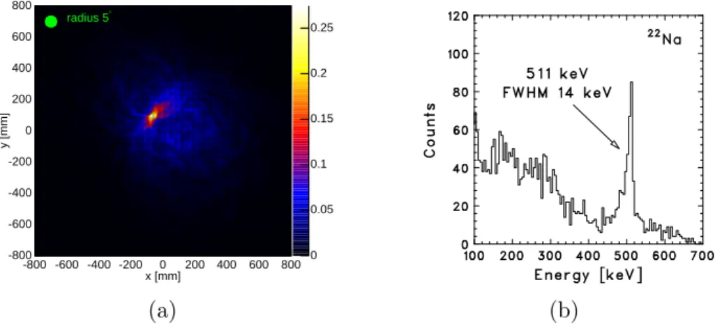
Fig. 9 (a) shows the Compton reconstructed images a of22Na 511 keV
gamma-ray source obtained with the prototype. The selected energy regions are 500– 520 keV. From the calculated scattering angle and the two-hit positions, a Compton cone is drawn on the sky on an event by event basis. We project the cone onto the plane at the distance of 350 mm, and obtain the image of the gamma-ray source. A circle with a radius of 5 degree is drawn together with each image as reference. We note that the images are asymmetric because the arrangement of CdTe absorbers is not symmetric. Fig. 9 (b) shows the reconstructed spectrum for 511 keV gamma-rays the 22Na gamma-ray source.
esti-x [mm]
-800 -600 -400 -200 0 200 400 600 800
y [mm] -800 -600 -400 -200 0 200 400 600 800 0 0.05 0.1 0.15 0.2 0.25 ° radius 5 (a) (b)
Fig. 9. Compton reconstructed image (left) and spectrum (right) of the 511 keV gamma-ray obtained with a prototype Si/CdTe Compton telescope. The angular resolution is 3.9 degree. The energy resolution is 14 keV (FWHM) at 511 keV[29]. A circle with a radius of 5 degree is drawn as reference in the image.
mated values (∆θDB) from the simulation. The scattering angle is determined
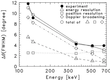
with a resolution of 3.9 degree (FWHM) at 511 keV. The effect of the Doppler broadening becomes smaller as the incident energy becomes higher, because the binding energy and momentum of electrons in materials become relatively small for gamma-ray photons with higher energies. In the same figure, the effect of ∆θposition, ∆θenergy and ∆θDopplerBroadening:
∆θtotal = √
(∆θposition)2+ (∆θenergy)2+ (∆θDopplerBroadening)2 (1)
are plotted together with the experimental data as ∆θtotal [29]. The
experi-mental values can be explained by the three contributions. In most cases, the angular resolution is limited by the effect of Doppler broadening, except that the contribution of position resolution is comparable to that of Doppler broad-ening in the higher energy region (>500 keV). According to the analysis based on Monte Calro detector simulation, we confirmed the contribution of Doppler broadening is 2.6 degree, and the contributions from position resolution and energy resolution are 2.6 degree and 2.7 degree, respectively[29] Additionally, CdTe layers can also be used as scatterer if the energy of incident gamma-rays is high. According to our measurements, the obtained angular resolution is 35.9 degree at 122 keV, and 12.2 degree at 511 keV, which is mainly domi-nated by the effect of Doppler broadening[31].
When kinetic energy of an electron is above∼ 250 keV, the range of electrons
Fig. 10. Relation between incident gamma-ray energy and angular resolution. Filled circles show the experimental data. Open triangles, squares and diamonds are esti-mated contributions of detector energy resolution, detector position resolution and Doppler broadening, respectively. The totals obtained by adding the three estimated values in quadrature are plotted by open circles[29]
.
smeared out by the effect of multiple scattering, we can limit the direction of incident gamma-rays as an arc, not a cone.
In the calculation of Compton kinematics, the angles between the direction of recoil electrons and that of scattered gamma-rays can be used to reject background events, especially for those in which the scattered gamma-rays are not fully absorbed in CdTe. Fig. 11 shows the reconstructed image of 662 keV gamma-rays from 137Cs from events that satisfy the consistency of the angle
between the electron and the scattered photon, which can be calculated either geometrically from hit positions or from the deposited energy [30]. In drawing the image, the width and the length of each arc are evaluated from the energy resolution and position resolution of the component detectors.
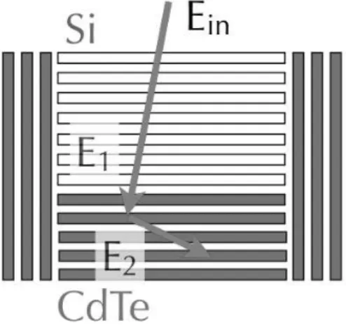
6 Narrow FOV Si/CdTe Compton Telescope
x [mm]
-800 -600 -400 -200 0 200 400 600 800
y [mm] -800 -600 -400 -200 0 200 400 600 800 0 1 2 3 4 5 ° radius 5
Fig. 11. An image of137Cs obtained from the Compton reconstruction with electron
tracking[30].
shield and collimator [23,24].
In order to further reduce the background and thus to improve the sensitivity, we have proposed a new detector called the Soft Gamma-ray Detector (SGD) for the NeXT mission. The SGD is a Si/CdTe semiconductor Compton tele-scope mounted inside the bottom of a well-type active shield[8,25,17,21,3]. As shown schematically in Fig.12, the telescope consists of 24 layers of DSSDs (double-sided silicon strip detectors) surrounded by CdTe pixellated detec-tors. The opening angle provided by the BGO shield is 4 degrees at 500 keV. For the SGD, an additional copper collimator restricts the field of view of the telescope to 30’ for low energy photons (<100 keV) to minimize the flux due to the Cosmic X-ray Background from within the FOV. These modules are then arrayed to provide the required area.
The major advantage of employing a narrow FOV is that the direction of inci-dentγ-rays is constrained to be inside the FOV. If the Compton ring does not intercept the FOV, we can reject the event as background. Most backgrounds can be rejected by requiring this condition (albeit with a corresponding re-duction in instrument effective area). Background photons from the BGO and copper collimator for which the reconstructed Compton ring intersects the FOV cannot be eliminated if there is no signal detected in the active shield, however this source of background contributes only within a limited range of scattering angle. Combining background suppression techniques available in the SGD, we expect to achieve background levels of 5×10⁻⁷ counts/s/cm2/keV
at∼100 keV and 2×10⁻⁷ counts/s/cm2/keV at∼500 keV. The effective area
of the SGD in the Compton mode is 120 cm2 at 200 keV and 50 cm2 at 400
keV, if we use 25 units (total geometrical area of 625 cm2).
Fig. 12. Conceptual design of the SGD module [3]. A stack of 24 Si DSSDs and CdTe pixel detectors are assembled to form a semiconductor Compton Telescope. The telescope is mounted inside the bottom of a well-type active shield. The open-ing angle provided by the BGO shield is 4 degrees at 500 keV. An additional copper collimator restricts the field of view of the telescope to 30’ for low energy pho-tons (<100 keV). With this narrow FOV, events are rejected as background if the
reconstructed Compton ring does not intercept the FOV.
which is a dominant background in the case of the uzaku HXD [24]. The 30’ FOV of the fine collimator is required to improve the sensitivity which is limited by source confusion below a few hundred keV. It should be noted that we can also measure polarization of incident gamma-rays from the azimuthal distribution of Compton scattered photons. The demonstration of the polar-ization measurement was performed by using a fully polarized synchrotron beam in the Spring 8 facility [?,32].
7 A narrow FOV Si/CdTe Compton Camera for the Gamma-ray lens mission
Focusing instruments have two tremendous advantages: first, the volume of the focal plane detector can be made much smaller than for non-focusing instruments, and second, the residual background, often time-variable, can be measured simultaneously with the source, and can be reliably subtracted. The MAX mission, which is based on the concept of Laue gamma-ray lens is very promising approach to extend the focusing capability above several hundred keV to reality.
plane detector should be designed very carefully. A Compton telescope is a good solution, because the direction of incident gamma-rays could be deter-mined by the Compton reconstruction and therefore effective in discriminating gamma-rays coming from the lens. However, the angular resolution limited by the Doppler broadening is 2.5 degrees for 511 keV and also the ordering of interactions has to be solved before we determine the direction of incident gamma-rays.
The concept of the narrow FOV Compton telescope realized with an active collimator made of BGO scintillator and a stack of Si/CdTe detector is a very attractive solution as the focal plane detector of the gamma-ray lens experiment. Fig. 13 shows the conceptual design of the focal plane detector. The FOV of the active collimator is determined such that it only sees the ray lens. With this, all we can assume is that the signal gamma-rays come from the FOV of the collimator, and others can be rejected as background. Furthermore a thick BGO scintillator shields gamma-rays from other directions and also reduces the background due to activation in the BGO scintillator itself. This is quite important, because the 511 keV line from the β+ decays becomes a major background source for the study of annihilation
lines from the celestial objects. The fact that the Si/CdTe Compton telescope can be operated at moderate temperatures of 0 to -20 degrees makes the design of the shield easy for satellite applications. The compact design of a stack of Si and CdTe detectors also helps, because, if the volume of the shield becomes large, the dead time caused by the shield becomes significant.
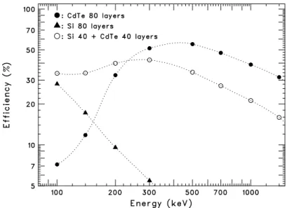
The effective area of the scattering part could be a concern. As shown in Fig. 14, a stack of Si detectors with a total thickness of ∼ 5 cm corresponds to
τ=1 for Compton scattering. This number is ∼ 2 cm for CdTe. Although
CdTe detectors also act as the scatterer above 300 keV, the angular resolution is larger than 10 degrees. To have a sufficient number of layers with DSSD would be preferable in terms of the angular resolution. Depending on the energy of interest, the number of Si and CdTe layers and their ratio should be chosen. Fig. 15 shows the peak detection efficiency of events which undergo multi Compton scattering and final photo absorption in a 80 layer detector. The efficiency for the different numbers of Si and CdTe layers are shown as a function of photon energy. The dimensions of the detector are 25 cm × 25
cm and the thickness of each layer is 0.5 mm. Gamma-rays are injected to the center of the top layer.
8 Conclusion
Fig. 13. Conceptual drawing for the focal plane detector for a gamma-ray lens mission.
Fig. 14. Thickness of the detector which corresponds toτCompton=1 for silicon and
CdTe.
become very difficult. Gamma-ray focusing technology should change this sit-uation considerably.
We have proposed a new detector called the Soft Gamma-ray Detector (SGD) for the NeXT mission, which utilizes the idea of a narrow FOV Si Compton telescope. In the SGD, we combine a stack of Si strip detectors and CdTe pixel detectors, to form a Compton telescope, which is mounted inside the bottom of a well-type active shield. We have demonstrated Compton reconstruction by using a prototype Si/CdTe Compton telescope, consisting of six-layered DSSDs and three 8 × 8 CdTe pixel detectors. By using this prototype, we
Fig. 15. Simulated peak detection efficiency for events which interact more than twice in the detector volume (more than one Compton scattering and final pho-to-absorption). The detector consists of 80 layers of thin Si or CdTe detector. The results are shown for CdTe layers only (filled circles), Si layers only (filled trian-gls) and mixture (open circles). Dimensions of each layer are 25 × 25 cm2 with a
thickness of 0.5 mm2. Gamma-rays are injected at the center of the top layer.
122 keV to 662 keV. The achieved energy resolutions are 9.1 keV and 14 keV at 356 keV and 511 keV, respectively. The angular resolution is 3.9 degrees (FWHM) for 511 keV gamma-ray photons.
The concept of the narrow FOV Compton telescope becomes a very attractive solution for the focal plane detector of the gamma-ray lens experiment. In order to obtain sufficient efficiency for 511 keV lines for the future mission, we are now working on the larger scale model of the Si/CdTe Compton telescope with several tens of layers of DSSD and CdTe pixel detectors.
Acknowledgement
References
[1] N. Gehrels and J. Paul, Physics Today, 51, 2, 26 (1998).
[2] T. Takahashi, K. Mitsuda, H. Kunieda, “The NeXT Mission”, Proc. SPIE, in press, 2006
[3] T. Takahashi, et al., “Wide band X-ray Imager (WXI) and Soft Gamma-ray Detector (SGD) for the NeXT Mission,” Proc. SPIE, vol. 5488, pp.549-560, 2004.
[4] T. Takahashi and S. Watanabe “Recent Progress on CdTe and CdZnTe detectors,” IEEE Trans. Nucl. Sci., vol. 48, pp. 950-959, 2001.
[5] O. Limousing, C. Blondel, J. Cretolle, H. Dzitko, P. Laurent, F. Lebrun, J.P. Leray, et al. “The ISGRI CdTe gamma-ray camera first steps,” Nucl. Instr. Meth., vol. A442, pp. 244-249, 2000.
[6] G. Sato, A. Parsons, D. Hullinger, M. Suzuki, T. Takahashi, M. Tashiro, K. Nakazawa et al. “Development of a Spectral Model Based on Charge Transport for the Swift/BAT 32K CdZnTe Detector Array,”Nucl. Instr. Meth., vol. A541, pp. 372-384, 2005.
[7] T. Takahashi, S.Watanabe, G.Sato, Y.Okada, S.Kubo, Y.Kuroda, M. Onishi, R. Ohno, “High Resolution CdTe Detector and Applications to Imaging Devices ,” IEEE Trans. Nucl. Sci., vol. 48, No. 3, pp. 287-291, 2001.
[8] T. Takahashi, K. Nakazawa, T. Kamae, H. Tajima, Y. Fukazawa, M. Nomachi, and M. Kokubun , “High resolution CdTe detectors for the next generation multi-Compton gamma-ray telescope ,” Proc. SPIE, vol. 4851, pp. 1228-1235, 2002.
[9] C. Matsumoto, T. Takahashi, K. Takizawa, R. Ohno, T. Ozaki, K. Mori, “Performance of a New Schottky CdTe Detector for Hard X-ray Spectroscopy,” IEEE Trans Nucl. Sci., 45, 428, 1998.
[10] T. Takahashi, K. Hirose, C. Matsumoto, K. Takizawa, R. Ohno, T. Ozaki, K. Mori, Y. Tomita, “Performance of a New Schottky CdTe Detector for Hard X-ray Spectroscopy,” Proc. SPIE, vol. 3446, pp. 29-37, 1998.
[11] M. Funaki, T. Ozaki, K. Satoh, and R. Ohno, “Growth and Characterization of CdTe Single Crystal for Radiation Detectors,” Nucl. Instr. Meth. , vol. A436, pp. 120-126, 2000.
[12] T. Takahashi, B. Paul, K. Hirose, C. Matsumoto, R. Ohno, T. Ozaki, K. Mori, Y. Tomita, “High-resolution Schottky CdTe Detectors for Hard X-ray and Gamma-ray Observations ,”Nucl. Instr. Meth. vol. A436 pp.111-119, 2000.
[14] K. Nakazawa, K. Oonuki, T. Tanaka, Y. Kobayashi, K. Tamura, T. Mitani, G. Sato, S. Watanabe, T. Takahashi, R. Ohno, A. Kitajima, Y. Kuroda and M. Onishi, “Improvement of the CdTe Diode Detectors using a Guard-ring Electrode,” IEEE Trans. Nucl. Sci, vol.51,No.4,pp.1881-1885, 2004.
[15] T. Tanaka, Y. Kobayashi, T. Mitani, K. Nakazawa, K. Oonuki, G. Sato, T. Takahashi and S. Watanabe, “Recent achievements of the high resolution Schottky CdTe diode for gamma-ray detectors,” New Astronomy Reviews, 48, pp. 269-273, 2004.
[16] Amptek Inc., http://www.amptek.com
[17] T. Takahashi, K. Nakazawa, S. Watanabe, G. Sato, T. Mitani, T. Tanaka, K. Oonuki, K. Tamura, H. Tajima, T. Kamae, G. Madejski, M. Nomachi, Y. Fukazawa, K. Makishima, M. Kokubun, Y. Terada, J. Kataoka, M. Tashiro, “Application of CdTe for the NeXT Mission”, Nucl. Instr. Meth. A, 541, pp. 332-341, 2005 .
[18] S. Watanabe, T.Takahashi, Y. Okada, G. Sato, M. Kouda, T. Mitani, Y. Kobayashi, K. Nakazawa, Y. Kuroda, M. Onishi, “CdTe stacked detectors for Gamma-ray detection”, IEEE Trans. Nucl. Sci.,vol. 49, No. 3, pp.1292-1296, 2002.
[19] S. Watanabe, T. Takahashi, K. Nakazawa, Y. Kobayashi, Y. Kuroda, K. Genba, M. Onishi, K. Otake , “A stacked CdTe Gamma-ray Detector and its application as a range finde,” IEEE Trans. Nucl. Sci., vol. 49, No. 3, pp. 1297-1303, 2002. [20] H. Tajima, T. Nakamoto , T. Tanaka , S. Uno , T. Mitani , E. do Couto
e Silva, Y. Fukazawa, T. Kamae, G. Madejski, D. Marlow, K. Nakazawa, M. Nomachi, Y. Oakada, T. Takahashi, “Performance of a low noise front-end ASIC for Si/CdTe detectors in Compton gamma-ray telescope,” IEEE Trans. Nucl. Sci., 51, pp. 842-847, 2004.
[21] H. Tajima, T. Kamae, G. Madejski, T. Mitani, K. Nakazawa, T. Tanaka, T. Takahashi, S. Watanabe, Y. Fukazawa, T. Ikagawa, J. Kataoka, M. Kokubun, K. Makishima, Y. Terada, M. Nomachi and M. Tashiro, “Design and Performance of Soft Gamma-ray Detector for NeXT mission”, IEEE Trans. Nucl. Sci., in press, 2005.
[22] T. Mitani,T. Tanaka, K. Nakazawa, T. Takahashi, T. Takashima, H. Tajima, H. Nakamura, M. Nomachi, T. Nakamoto, Y. Fukazawa,“A Prototype Si/CdTe Compton Camera and the Polarization Measurement , ” IEEE Trans. Nucl. Sci., pp.2432-2437, 2004.
[23] T. Kamae et al., “Astro-E hard X-ray detector,” Proc. SPIE, vol. 2806, pp. 314-328, 1996
[24] M. Kokubun et al.,“Improvements of the Astro-E2 Hard X-ray Detector (HXD-II), ” IEEE Trans. Nucl. Sci., v51,pp.1991, 2004
detectors for the NeXT mission,”, New Astronomy Reviews, 48, pp. 309-313, 2004.
[26] H. Tajima, T. Kamae, S. Uno, T. Nakamoto, Y. Fukazawa, T. Mitani, T. Takahashi, K. Nakazawa, Y. Okada, and M. Nomachi, “Low noise double-sided silicon strip detector for multiple-Compton gammaray telescope,” Proc. SPIE, vol. 4851, pp. 875-884, 2002
[27] T. Tanaka, T. Mitani, S. Watanabe, K. Nakazawa, K. Oonuki, G. Sato, T. Takahashi, K. Tamura, H. Tajima, H. Nakamura, M. Nomachi, T. Nakamoto, Y. Fukazawa, “Development of a Si/CdTe semiconductor Compton telescope ”, Proc. SPIE, vol. 5501, pp. 229-240, 2004.
[28] Y. Fukazawa, T. Nakamoto, N. Sawamoto, S. Uno, T. Ohsugi, H. Tajima, T. Takahashi, T. Mitani, T. Tanaka, K. Nakazawa, “Low-noise double-sided silicon strip detector for soft gamma-ray Compton camera,” Proc. SPIE, vol. 5501, pp. 197-207, 2004
[29] S. Watanabe, T.Tanaka, K. Nakazawa, T. Mitani, K. Oonuki, T. Takahashi, T. Takashima, H. Tajima, Y. Fukazawa, M. Nomachi, S. Kubo, M. Onishi, Y. Kuroda, “A Si/CdTe Semiconductor Compton Camera,” IEEE Trans. Nucl. Sci., 52, pp.2045-2051, 2005.
[30] T. Tanaka, S. Watanabe, S. Takeda, K. Oonuki, T. Mitani, K. Nakazawa, T. Takashima, T. Takahashi, H. Tajima, N. Sawamoto, Y. Fukazawa, M. Nomachi, “Recent results from a Si/CdTe semiconductor Compton telescope,” NIM A, in press, 2006.
[31] K. Oonuki, T. Tanaka, S. Watanabe, S. Takeda, K. Nakazawa, T. Mitani, T. Takahashi, H. Tajima, Y. Fukazawa, M. Nomachi, “Results of a Si/CdTe Compton telescope,” Proc. SPIE, vol. 5922, pp. 78-88, 2005

![Fig. 12. Conceptual design of the SGD module [3]. A stack of 24 Si DSSDs and CdTe pixel detectors are assembled to form a semiconductor Compton Telescope](https://thumb-ap.123doks.com/thumbv2/123deta/6860052.243761/13.892.290.608.109.433/conceptual-design-module-detectors-assembled-semiconductor-compton-telescope.webp)