A Test Generation Method for State Observable FSMs to Increase Defect Coverage
under the Test Length Constraint
Ryoichi INOUE Toshinori HOSOKAWA and Hideo FUJIWARA
Graduate School of Industrial Technology, Nihon University 1-2-1, Izumicho, Narashino, Chiba 275-8575, Japan College of Industrial Technology, Nihon University 1-2-1, Izumicho, Narashino, Chiba 275-8575, Japan
Graduate School of Information Science, Nara Institute of Science and Technology (NAIST) 8916-5, Takayama, Ikoma, Nara 630-0192, Japan
E-mail: [email protected], [email protected], [email protected]
Abstract
Since scan testing is not based on the function of the circuit, but rather its structure, scan testing is considered to be a form of over testing or under testing. It is important to test VLSIs using the given function. Since the functional specifications are described explicitly in the FSMs, high test quality is expected by performing logical testing and timing testing. This paper proposes a test generation method to detect specified fault models completely and to increase defect coverage as much as possible under test length constraint. We give experimental results for MCNC’91 benchmark circuits. The proposed test generation method achieves high bridging fault coverage, high transition fault coverage, and high path delay fault coverage compared to the conventional fault-dependent test generation method.
keywords: state-observable FSMs, logical testing, timing testing, n-detection
1. Introduction
In recent years, very large scale integrated circuit (VLSI) testing has become increasingly important because the number of gates on VLSIs is increasing rapidly and the complexity of VLSIs is growing with advances in semiconductor technology. Currently, scan testing for the stuck-at fault model [1, 2] is one of the most popular test methods for VLSIs. However, it has been reported that scan testing for the stuck-at fault model may not detect defective VLSIs [4], and delay testing and at-speed functional testing can effectively improve test quality [3]. As mentioned above, scan testing is currently the most popular test method. Scan testing is based on the structure of the circuit rather than its function and generates test pattern. In scan testing, the states of the circuits are transferred to invalid states by the shift operation during the testing in order to detect faults. This method is considered to be a form of over testing
and yield loss of VLSIs may occur. Scan testing also detects faults by shifting-in, the operation of a combinational circuit part, and shifting-out. Hence, faults are not detected by performing sequential operations of the circuits. This testing is considered to be a form of under testing. Therefore, the test quality deteriorates, and outflow of defective VLSIs into the market may occur.
VLSI design methodologies using hardware description languages have recently been adopted to reduce VLSI design time. VLSIs are designed at the Register Transfer Level (RTL), and RTL circuits consist of a data path part and a controller part. The data path contains a hardware element (e.g., registers, multiplexers, and operational modules) and signal lines. The controller is represented by a finite state machine (FSM). A controller and a data path are interconnected by internal signals: control signals and status signals. A non-scan-based Design For Testability (DFT) method of the data path part is proposed in [5], whereas a non-scan-based DFT method for the controller part is proposed in [6]. At-speed testing is possible, and test patterns for a stuck-at fault model are completely generated by non-scan-based DFT methods. In [5, 6], both control signals from a controller and status signals from a data path were assumed to be directly controllable from primary inputs and observable at primary outputs. As mentioned above, if at-speed functional testing and/or delay testing are applied to VLSIs with a non-scan-based DFT, the test quality can be further improved. As for the FSM, which is the controller part of an RTL circuit, the circuit specification is described explicitly. Thus, it is expected that the test quality becomes high by performing a logical testing and a timing testing under the constraints of the circuit specifications.
In consideration of these tests, a fault-independent one-pattern test generation method and a fault-independent two-pattern test generation method that enable a complete logical testing and a timing testing have been proposed [7,8]. However, when the number of state transitions increases, the test length drastically increases. It is necessary to detect a IEEE 8th Workshop on RTL and High Level Testing (WRTLT'07), pp. 79-86, October 2007.
specified fault model (e.g. stuck-at fault) completely and to detect main fault models such as bridging fault, transition fault, and path delay fault as much as possible for state-observable FSMs. It was reported that an n-detection test generation method (FSOD) to increase the fault sensitization coverage [9] comparatively detected many bridging faults and transition faults.
This paper proposes a test generation method to detect specified fault models completely and to increase defect coverage as much as possible under test length constraint. This paper also proposes weighted state transition coverage as a measure of test quality.
This paper is organized as follows. In Section 2, the definition of state-observable FSMs. In Section 3, the detection conditions of main fault models and an n-detection test generation method to increase defect coverage are described. In Section 4, a test generation method for state-observable FSMs is proposed, and experimental results for MCNC’91 FSM benchmarks [10] with many state transitions are discussed in Section 5. Finally, Section 6 concludes the paper and discusses future research possibilities.
2. State-observable FSMs
(Definition 1: State-observable FSMs)
When an initial state can be identified by observing an output sequence without being dependent on the input sequence, the FSM is said to be state-observable. More specifically, when an initial state can be identified by observing an output sequence of length k, the FSM is said to be k state-observable.
Figure 1 shows an example of an FSM. In this figure, ST0 through ST5 and T0 through T11 show the states and the input values, respectively, of the state transitions (the value of each primary input ∈ {0, 1, X}, where X denotes don’t care). The DFT transformed an FSM to a one-state observable FSM by making the outputs of the status registers in the FSM observable. In this paper, a one-state observable FSM is hereinafter referred to simply as a state observable FSM. A synchronous sequential circuit is synthesized from the FSM by logic synthesis. Figure 2 shows the logic circuit model that corresponds to the FSM after logic synthesis. Since the pseudo primary inputs (PPI), which are the outputs of the status registers, are observable in this figure, the PPIs connect with the primary output. Thus, multiplexers are added on the PPI and are connected to the primary outputs of the data path in order to reduce the overhead of primary output pins [11]. Here, PI, PO, SR, PPI, PPO, and R denote the primary inputs, primary outputs, status registers, pseudo primary inputs (outputs of the status registers), pseudo primary outputs (inputs of the status registers), and a reset input, respectively.
In the test of state-observable FSMs, the PI value is applied to a state-observable FSM, the resulting PO values are observed, the state is then transferred from the current state to the next state, and the resulting PPI values are observed. A series of these procedures is referred to as a test for
state-observable FSMs.
Example 1: In Fig. 1, T0 is applied to state ST0 on the state-observable FSM and the state is transferred from ST0 to ST1. T1 is then applied, and the state is transferred from ST1 to ST2. Next, test for the state-observable FSM is explained in detail. R is activated and the values of the status registers are initialized to ST0 in the first cycle. In the second cycle, T0 is applied and the values of the POs for (PI, PPI) = (T0, ST0) are observed just before the rising edge of the clock. Here, (PI, PPI) denotes that the value of PI is applied to the PPI value (state) for the state-observable FSM. Moreover, the PPI value is observed after the rising edge of the clock. Thus, it is verified that the state is successfully transferred from ST0 to ST1. In the third cycle, T1 is applied and the PO values for (PI, PPI) = (T1, ST1), which are observed just before the rising edge of the clock. The resulting PPI value is observed after the rising edge of the clock. Thus, it is verified that the state is successfully transferred from ST1 to ST2.
The FSM has a completely specified FSM [14], in which the next state and the output are specified for all of the inputs of each state, and an incompletely specified FSM [11], in which the next state and the output are not specified for all of the inputs of each state. In this paper, in the incompletely specified FSMs, state transitions that are not specified are assumed to be the same as either of the state transitions that are specified.
ST0
ST1
ST4
ST3
ST5
ST2 T0
T1 T3
T4 T5
T10
T7
T9 T2
T6
T11
T8
Fig. 1 Example of an FSM (six states)
Combinational Circuit
PO PI
State-Observable
SR
PPI PPO
PO PI
Combinational Circuit
R SR
PPI PPO
R
State-Observable
Fig. 2 Logic model for a state-observable FSM
3. Detection Conditions for Each Fault Model First, an n-detection test generation method to increase fault sensitization coverage [9] is described. Next, detection conditions for the main fault models such as bridging faults [2], transition faults [3], and path delay faults [3] are described.
3.1. An n-Detection Test Generation Method to Increase Fault Sensitization Coverage
(Definition 2: Fault Sensitization Coverage)
Fault sensitization coverage for fault f is defined as the ratio of the number of signal lines sensitized by test set T to the number of all signal lines that are reachable from f. Here, sensitized signal lines for f are lines on the fault propagation path at the time that f is detected. Fault sensitization coverage for the whole circuit is expressed by the average value of fault sensitization coverage for all faults. The formulas of fault sensitization coverage for f and the whole circuit are expressed as follows.
・senf :Fault sensitization coverage for fault f f 100
senf = ×
from reachable are which lines signal the of Number
lines signal sensitized of
Number (1)
・SEN:Fault sensitization coverage for the whole circuit
faults of Number
=
∑
senfSEN (2)
An n-detection test generation method to increase fault sensitization coverage, FSOD can be used for stuck-at faults to increase fault sensitization coverage based on the following strategies.
(1) For each fault, FSOD generates n test patterns that sensitizes different fault propagation path and detects faults.
(2) FSOD selects D-frontier[1, 2] to sensitize long fault propagation path segments.
3.2. Detection of Bridging Faults
A bridging fault is a fault model that expresses a short between signal lines. Bridging faults are classified into AND type and OR type based on failure behavior. It is necessary to generate a test pattern that detects a stuck-at 0 (1) fault for one signal line and sets 0 (1) to the other signal line in order to detect an AND (OR) type bridging fault. In this paper, U model [12] is used. Both an AND type and an OR type must be detected for the detection of a U model of the bridging fault. A bridging fault may be able to be detected only when it sensitizes a specific path. Therefore, if test patterns are generated so that many paths are be sensitized as much as possible, bridging fault coverage is increased. Since FSOD sensitizes many fault propagation paths by increasing fault sensitization coverage, it is consider that the generated test
patterns achieve high bridging fault coverage.
3.3. Detection of Transition Faults
A transition fault model assumes that a delay fault affects only one signal line in the circuit. There are two transition faults associated with each signal line: a slow-to-rise fault and a slow-to-fall fault. It is assumed that in the fault-free circuit each signal line has some nominal delay. Delay faults results in an increase of this delay. Under the transition fault model, the extra delay caused by the delay fault is assumed to be large enough to prevent the transition from reaching any primary output at the time of observation. In other words, the transition fault can be observed independent of whether the transition propagates through a long or short path to any primary output. To detect a transition fault, it is necessary to apply a test pattern pair, V = (v1, v2). For testing a slow-to-rise (a slow-to-fall), the first pattern, v1, initializes the fault site to 0 (1), and the second pattern, v2, is a test pattern for stuck-at-0 (1) fault at the fault site. It is considered that FSOD can detect a small size of delay fault because it sensitizes a long fault propagation path to increase fault sensitization coverage. Because FSOD also generates n-detection test patterns, transition probability of fault sites between the first pattern and the second pattern is high. Then, the probability of transition fault detection is considered to increase.
3.4. Detection of Path Delay Faults
Under a path delay fault model, a combinational circuit is considered faulty if the delay of any of its paths exceeds a specified limit. A path is defined as an ordered set of gates {g0, g1, ...., gn}, where g0 is a primary input or a FF, and gn is a primary output or a FF. A delay defect on a path can be observed by propagating a transition through the path. There exist several classes of path delay faults according to the sensitization criteria. In this paper, a non-robust testable path delay fault [3] is dealt with. There are two transition faults associated with each path: a slow-to-rise fault and a slow-to-fall fault. In order to detect a non-robust testable path delay fault, it is necessary to apply a test pattern pair, V = (v1, v2). In order to test a slow-to-rise (slow-to-fall) fault, the first pattern, v1, initializes the primary inputs or the FFs on the path to 0 (1), and the second pattern, v2, is a test pattern for stuck-at-0 (1) fault at the primary inputs or the FFs on the path. Moreover, v2 must propagate the fault effect through the path. FSOD also generates test patterns to increase fault sensitization coverage for faults at primary inputs. Thus, since the probability that many paths are sensitized is high, it is considered that the generated test patterns may be able to detect many path delay faults. Since FSOD also generates n-detection test patterns, transition probability of a primary input (or a FF) between the first pattern and the second pattern is high. Thus, the probability of path delay fault detection increases.
4. Test Generation Method for State-observable FSMs
This method generates a test sequence by generating an FSM test generation graph from state-observable FSMs and searching for a path. We propose weighted one-state transition coverage and weighted two-state transition coverage as measures of test quality for logical testing and timing testing, respectively, for the generated test sequence.
4.1. FSM Test Generation Graph
(Definition 3: FSM test generation graph)
An FSM test generation graph is a directed graph G(V, E, s, d, t), where a vertex v ∈ V denotes a state transition. Each vertex has a label s: V → A (A = {PPI1PPI2 … PPIm}, PPI1, PPI2, …, PPIm ∈ {0, 1}, where m denotes the number of status registers), a label d: V → A (A = {PPI1PPI2
… PPIm}, PPI1, PPI2, …, PPIm ∈ {0, 1}, and a label t: V
→ B (B = {PI1PI2 …PIn}, PI1, PI2, …, PIn ∈ {0, 1}, where n denotes the number of primary inputs). The label s indicates the source state of the state transition, the label d indicates the destination state of the state transition. The label t indicates input values for the state transition. For any vertices u, v ∈ V, an edge (u, v) ∈ E indicates that the destination state in u is the same as the source state in v. The edge (u, v) represents a continuous state transition pair. Furthermore, the weights are assigned to each vertex and edge. The weight of a vertex, wv(v) (v ∈ V) is 1 if {s, t} in v is equivalent to test patterns that are generated by FSOD, and otherwise 0. Here, {s, t} denotes the concatenation of s and t. The weight of an edge, we((v1,v2)) (v1,v2 ∈ V, (v1,v2) ∈ E) is the Hamming distance between {s, t} in v1 and {s, t} in v2, if wv(v2) is 1. If wv(v2) is 0, then we((v1, v2)) is 0.
The quality of logical testing is considered to increase by executing test patterns generated by FSOD. Therefore, the weight wv is assigned to the vertex. The transition between the first pattern and the second pattern must occur at a primary input or an FF on a path in order to increase the quality of path delay fault testing. Thus, when the Hamming distance between the first pattern and the second pattern is large, the probability that the transition occurs is high. It has been reported that when the number of transitions at primary inputs is large, the number of transition at internal signal lines is also large [13]. Thus, the probability for the detection of transition faults becomes high.
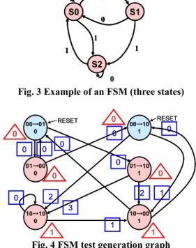
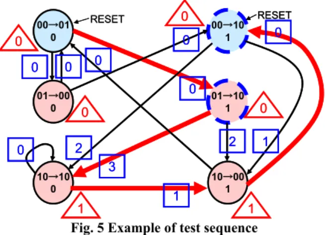
Example 2: Figure 3 shows the state-observable FSM. Figure 4 shows the FSM test generation graph of Figure 3. The two test patterns, (PPI1,PPI2,PI) = (1,0,0) and (PPI1,PPI2,PI) = (1,0,1), are generated for the combinational circuit after logic synthesis by the FSOD. In Figure 4, a state assignment code of
S0 S1
S2 0 0
1 0
1 1 RESET
S0 S1
S2 0 0
1 0
1 1 RESET
Fig. 3 Example of an FSM (three states)
00→01 0
00→10 1
01→00 0
01→10 1
10→10 0
10→00 1
RESET RESET
2 3
0 2 1
1
1 1
0 0
0
0
0
0
0 0
0 0
00→01 0
00→10 1
RESET RESET
01→00 0
01→10 1
10→10 0
10→00 1
2 3
0 2 1
1
1 1
0 0
0
0 0 0
0
0 0 0
Fig. 4 FSM test generation graph
the source state (label s), a state assignment code of the destination state (label d), and the input value in each vertex corresponding to a state transition are assigned. Moreover, the weight wv is assigned to each vertex and the weight we is assigned to each edge. In Figure 4, triangles indicate the values of wv and a squares indicate the values of we. Each vertex is expressed as (s, d, t). The edge ((00, 01, 0), (01, 10, 1)) means that the state 00 transfers to the state 01 by the input 0 and the state 01 transfers to the state 10 by the input 1. Since the test pattern generated by FSOD, (PPI1,PPI2,PI) = (1,0,0), corresponds to the vertex (10, 10, 0), the wv is 1. Similarly, since the test pattern generated by FSOD, (PPI1,PPI2,PI) = (1,0,1), corresponds to the vertex (10, 00, 1), the wv is 1. In other vertices, wvs are 0. In the edge ((01, 10, 1), (10, 10, 0)) of we is assigned 3 that is the Hamming distance between (PPI1,PPI2,PI) = (1,0,0) is generated by FSOD and (s, d) = (01, 1) of the start vertex (01, 10, 1). In the edge ((00, 10, 1), (10, 10, 0)) of we is assigned 2 that is the Hamming distance between (PPI1,PPI2,PI) = (1,0,0) is generated by FSOD and (s, d)=(00, 1) of the start vertex (00, 10, 1). In the edge ((10, 10, 0), (10, 10, 0)) of we is assigned 0 that is the Hamming distance between (PPI1,PPI2,PI) = (1,0,0) is generated by FSOD and (s, d) = (10, 0) of the start vertex (10, 10, 1). Likewise, in the edge ((00, 10, 1), (10, 00, 1)) of we is assigned 1 that is the Hamming distance between (PPI1,PPI2,PI) = (1,0,1) is generated by FSOD and (s, d) = (00, 1) of the start vertex (00, 10, 1). In the edge ((01, 10, 1), (10, 00, 1)) of we is assigned 2 that is the Hamming distance between (PPI1,PPI2,PI) = (1,0,1) is generated by FSOD and (s, d) = (01, 1) of the start vertex (01, 10, 1). In the edge ((10, 10, 0), (10, 00, 1)) of we is assigned 1 that is the Hamming
distance between (PPI1,PPI2,PI) = (1,0,1) is generated by FSOD and (s, d)=(10, 0) of the start vertex (10, 10, 0). In the other edges, we is 0.
4.2. Weighted State Transition Coverage
Weighted one-state transition coverage and weighted two-state coverage are calculated using the weights assigned to the vertices and the edges in the FSM test generation graph. (Definition 4: Weighted one-state transition coverage) The Weighted one-state transition coverage is expressed in equation (3) and is used as a measure of the test quality for logical testing.
100(%) vertices
all for weights of Sum
sequence by test covered vertices of weights of Sum
coverage n transitio state - one Weighted
×
=
(3)
(Definition 5: Weighted two-state transition coverage) The Weighted two-state transition coverage is expressed in equation (4) and is used as a measure of the test quality for timing testing.
{
The weightsofinput edgesfor each vertex v}
100(%)max
sequence by test covered which
x v each verte for
edges input of weight max The
coverage n transitio state - two Weighted
⎭×
⎬⎫
⎩⎨
⎧
=
∑ ∑
v v
(4)
The following problem is formulated for the test generation for state-observable FSMs under test length constraint. (Formulation)
Input:
- a state-observable FSM.
- a test set that can detect all detectable stuck-at faults on valid states.
Constraint: test length
Output: a test sequence for the state-observable FSM such that all detectable stuck-at faults on valid states are detected. Optimization:
(1) maximization of weighted one-state transition coverage (2) maximization of weighted two-state transition coverage
The valid states are assigned to PPI values as constrains. FSOD is performed for the combinational circuit part to generate the test patterns. Then, an FSM test generation graph is generated and given stuck-at fault test pattern set are assigned to the corresponding vertices on the FSM test generation graph. Next, the test patterns generated by the FSOD are assigned to the corresponding vertices on the FSM test generation graph. Finally, paths are searched on the FSM test generation graph such that all of the edges on which stuck-at fault tests are assigned are traversed at least once. The traversal passes along vertices at which as many test patterns generated by the FSOD are assigned as possible, so as to
increase the weighted one-state transition coverage. The traversal also passes along the edges with the large possible weight, in order to increase the weighted two-state transition coverage. If all of stuck-at fault test patterns are not covered vertices under test constraint, it denotes no answer.
4.3. Strategy of Test Generation
The test generation strategy searches for all k state transitions from the current state in the FSM test generation graph. A state transition path is selected according to the following heuristics.
(Heuristics)
In the early stage of test generation, the probability that uncovered vertices, at which stuck-at test patterns are assigned, appear is high in k state transition path because the number of uncovered vertices is large. In this case, the state transitions path is selected by the priority of heuristics 3, 4, 5, 1, and 2. As the number of uncovered vertices, at which stuck-at test patterns are assigned, is small, the probability that the patterns appear in the k state transition path is low. When the number of uncovered vertices at which stuck-at test patterns are assigned is 0 continuously m times, the state transitions path is selected by the priority of heuristics 1, 2, 3, 4, and 5. Here, k and m are used as parameters.
Heuristic 1
The algorithm preferentially selects a path that includes many uncovered vertices where stuck-at test patterns are assigned. Heuristic 2
To reduce the test length, the algorithm preferentially selects a path such that the distance from the current state to uncovered vertices, where stuck-at test patterns are assigned, is short. Heuristic 3
To increase the quality of logical testing, the algorithm preferentially selects a path such that the total sum of wv is large. As a result, the weighted one-state transition coverage becomes high.
Heuristic 4
To reduce test length, the algorithm preferentially selects a path such that the distance from the current state to uncovered vertices, where test patterns generated by FSOD are assigned, is short.
Heuristic 5
In order to increase the quality of timing testing, the algorithm preferentially selects a path such that the total sum of we is large. As a result, the weighted two-state transition coverage becomes high.
00→01 0
00→10 1
01→00 0
01→10 1
10→10 0
10→00 1
RESET RESET
2 3
0 2 1
1
1 1
0 0
0
0
0
0 0
0 0
00→01 0
0
00→10 1
RESET RESET
01→00 0
01→10 1
10→10 0
10→00 1
2 3
0 2 1
1
1 1
0 0
0
0 0 0
0
0 0 0
Fig. 5 Example of test sequence
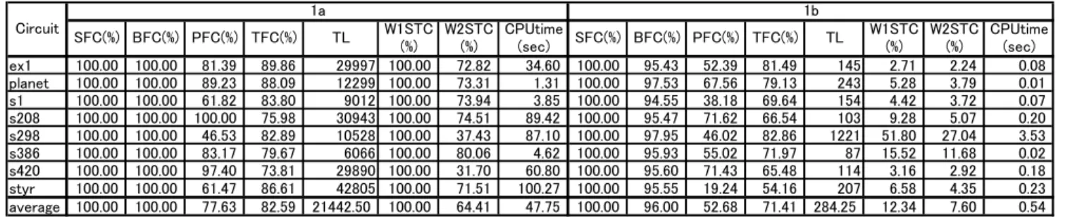
Example 3: Given the stuck-at test patterns, (PPI1,PPI2,PI) = (0,0,1), and (PPI1,PPI2,PI) = (0,1,1), Figure 5 shows the FSM test generation graph of Figure 3. FSOD generates the test patterns, (PPI1,PPI2,PI) = (1,0,0), and (PPI1,PPI2,PI) = (1,0,1). In Figure 5, the vertices indicated by dashed lines are vertices where stuck-at test patterns are assigned. When the test sequence (0, 1, 0, 1) is generated from the reset state, the weighted one-state transition coverage is 100% (2/2) whereas the weighted two-state transition coverage is 80 % ((3+1)/(3+2)=4/5).
5. Experimental Results
The test generation method was implemented and was applied to MCNC'91 benchmark circuits [10]. The characteristics of MCNC’91 benchmark circuits are shown in Table 1. In this table, Circuit, #Node, #PI, #PO, #Reg, and
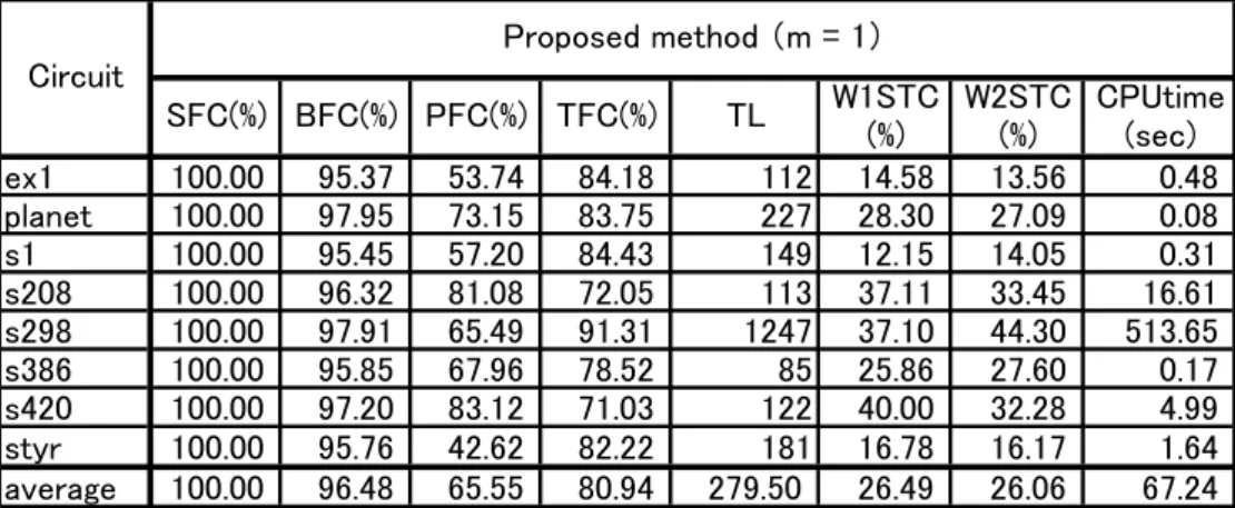
#Edge denote the circuit name of the FSM, the number of states, the number of primary inputs, the number of primary outputs, the number of status registers and the number of state transitions, respectively. In these experiments, the FSMs were made state observable by DFT, and three test generations were performed for state-observable FSMs. Table 2 shows the experimental results of fault-independent one-pattern test generation method (1a) [7,8] and the fault-dependent one-pattern test generation method (1b)[7,8]. Table 3 shows the experimental results of the proposed method when the value of m was set to one. This algorithm detects stuck-at faults completely, it stops. The value m is parameter for a switching timing of algorithm shown in the heuristic priority rules. Table 4 shows the experimental results of the proposed method when test length constraint was set to 300 and 500. The circuits indicated by the “*” symbol in the table were ones for which stuck-at fault could not be detected completely by the test lengths of 300 and 500. The value k was set to 3 in all experiments. Moreover, the value n of n-detection for FSOD was set to 5. In Tables 2, 3, and 4, Circuit, TL, and CPU time denote the circuit name of the FSM, the test length, and the time for the test generation, respectively. SFC, BFC, PFC, TFC, W1STC, W2STC, and FSC denote the stuck-at fault
coverage, the bridging fault coverage, the path delay fault coverage, the transition fault coverage, the weighted one-state transition coverage, and the weighted two-state transition coverage, respectively. Each logical testing targets only faults that can be detected on valid states [7]. Each timing testing targets only faults that can be detected on the transition between valid states [7,8].
First, the experimental results of the proposed method are considered when the value of m is one. Stuck-at faults can be completely tested. The weighted one-state transition coverage increased an average of 14.15%, and the weighted two-state transition coverage increased an average of 18.46% in the almost same test length compared to the fault-dependent one-pattern test generation method for the stuck-at fault model. Bridging fault coverage increased an average of 0.48%, and path delay fault coverage increased an average of 12.87%. In addition, transition fault coverage increased an average of 9.53%. In particular, for styr, the weighted one-state transition coverage increased 10.2%, bridging fault coverage increased 0.21%. Also, the weighted two-state transition coverage increased 11.82%, path delay fault coverage increased 23.38%, and transition fault coverage increased an average of 28.06%, and the quality of the timing testing was improved.
Next, the experimental results are considered for the proposed test generation with the test length constrains. Stuck-at fault could be completely tested and the test length was greatly reduced compared with the fault-independent one-pattern test generation method and high fault coverage for a bridging fault, a transition fault, and a path delay fault can be obtained. In particular, for s386, when test length constraint was set to 500, the weighted two-state transition coverage increased 8.42%, the path delay fault coverage increased 3.89% and the transition coverage increased 4.43%.
6. Conclusion
This paper proposed a test generation method to detect specified fault models completely and to increase defect coverage as much as possible under the test length constraint. This paper also proposed weighted state transition coverage as measures of test quality. The proposed test generation method was evaluated for MCNC '91 benchmark circuit and the following conclusions were obtained.
(1) The proposed test generation method increased the test quality of logical testing and the timing testing compared with the fault-dependent one-pattern test generation method.
(2) The proposed test generation method greatly reduced the test length compared with the fault-independent one-pattern test generation method and the quality of both the logical testing and the timing testing were comparatively high.
References [8] T. Hosokawa, R. Inoue, and H. Fujiwara, “Fault
Dependent/Independent Test Generation Methods for State Observable FSMs,” IEEE 7th Workshop on RTL and High Level Testing (WRTLT'06), pp. 13-18, November, 2006.
[1] H. Fujiwara, “Logic Testing and Design for Testability,” The MIT Press, 1985.
[9] T. Hosokawa and K. yamazaki, “An n-Detection Test Generation Method to Increase Fault Sensitization Coverage”, IEICE Trans. Info. and Syst.,Vol.J90-D, No. 6, pp. 1474-1482, June.2007 in Japanese. [2] M. Abramovici, M. A. Breuer, and A. D. Friedman, “Digital
systems testing and testable design,” IEEE Press, 1995.
[3] A. Krstic, and K. -T. Cheng, “Delay Fault Testing for VLSI
Circuits,” Kluwer Academic Publishers, 1998. [10] S. Yang, “Logic synthesis and optimization benchmarks user guide,” Technical Report 1991-IWLS-UG-Saeyang, Microelectronics Center of North Carolina, 1999.
[4]P. C. Maxwell, R. C. Aitken, R. Kollitz, and A. C. Brown, “IDDQ and AC Scan: The War Against Unmodelled Defects,” Proc. of IEEE
Int. Test Conf., pp.250-258, Oct., 1996. [11] S. Ohtake, H. Wada, T. Masuzawa and H. Fujiwara, " A non-scan DFT method at register-transfer level to achieve complete fault efficiency, " IEEE Proc. Asian South Pacific Design Automation Conference, pp.599-604, 2000.
[5]H. Wada, T. Masuzawa, K. K.Saluja, and H. Fujiwara, “Design for strong testability of RTL data paths to provide complete fault efficiency,” Proc. of 13th Int. Conf. on VLSI Design, pp.300-305,
2000. [12] Y. Takamatsu, T. Shiosaka, T. Yamada, and, K. Yamazaki, “A
Fault Model and Test Generation for Bridging Faults in CMOS Circuit,” IEICE Trans. Vol.J81-D, No.6, pp. 872-879, Jun.1998. [6]S. Ohtake, T. Masuzawa, and H. Fujiwara, "A non-scan approach
to DFT for Controllers Achieving 100% Fault Efficiency," Journal of Electronic Testing: Theory and Applications (JETTA), Vol. 16, No. 5, pp.553-566, Oct. 2000.
[13] S. Kajihara, K. Ishida, K. Miyase, “Average Power Reduction in Scan Testing by Test Vector Modification”, IEICE Trans. Info. and Syst.,Vol.E85-D, No. 10, pp. 1483-1489, Oct.2002.
[7] T. Hosokawa and H. Fujiwara, “A functional test method for state observable FSMs,” IEEE 6th Workshop on RTL and High Level Testing (WRTLT'05), pp.123-130, July 2005.
[14] T. Sasao, “Switching Theory for Logic Synthesis,” Kluwer Academic Publishers, 1999.
Table 1 FSM benchmark characteristics
# #
# # I #
Table 2 Experimental results for logical testing
. . . . . . . . . . . . . .
. . . . . . . . . . . . . .
. . . . . . . . . . . . . .
. . . . . . . . . . . . . .
. . . . . . . . . . . . . .
. . . . . . . . . . . . . .
. . . . . . . . . . . . . .
. . . . . . . . . . . . . .
. . . . . . . . . . . . . . . .
L W
% W
%
% % L % %
W
%
% %
W
%
% %
Table 3 Experimental results (m = 1)
. . . .
. . . .
. . . .
. . . .
. . . .
. . . .
. . . .
. . . .
. . . .
=
W
% L
%
W
%
% % %
Table 4 Experimental results (test length constraint)
. . . . . . . . . . . . . .
. . . . . . . . . . . . . .
. . . . . . . . . . . . . .
. . . . . . . . . . . . . .
. . . . . . . . . . . . . .
. . . . . . . . . . . . . .
. . . . . . . . . . . . . .
. . . . . . . . . . . . . .
. . . . . . . . . . . . . . . .
L = L =
% % % % L
W
% W
%
% % %
W
% W
%
% L