A Path Delay Test Generation Method for Sequential Circuits
Based on Reducibility to Combinational Test Generation
Tsuyoshi Iwagaki Satoshi Ohtake Hideo Fujiwara Graduate School of Information Science, Nara Institute of Science and Technology Kansai Science City 630-0192, Japan Tel: +81-743-72-5226 Fax: +81-743-72-5229
E-mail:{tsuyo-i, ohtake, fujiwara}@is.aist-nara.ac.jp
Abstract In this paper, we present a new structure, called discontinuous reconvergence structure (DR-structure), of se- quential circuits. We show that the path delay fault test gen- eration problem for sequential circuits with DR-structure can be reduced to the segment delay fault test generation problem for their time-expansion models, which are com- binational circuits. We propose a test generation method for path delay faults in sequential circuits with DR-structure based on the reducibility, and show the effectiveness of the method by a case study.
Keywords path delay fault, test generation, discontinu- ous reconvergence structure, time-expansion model, par- tially enhanced scan design
1 Introduction
With the increasing speed and complexity of VLSI cir- cuits, tests targeted only for stuck-at faults are insufficient to guarantee the proper circuit operation. Delay testing is necessary to reach the acceptable quality level. Until now, several delay fault models have been investigated [9]. The path delay fault model [11] is one of the most general mod- els among them because distributed faults along paths can be tested and the delay size of detectable faults is scalable.
In general, test generation for sequential circuits under simple fault models such as the single stuck-at fault model is itself a hard task. Path delay test generation for sequen- tial circuits is an even more challenging problem even if a small number of paths to be tested is selected by several path selection techniques [9]. For such sequential circuits, design for testability (DFT)is an important approach to re- duce the test generation effort. Given a sequential circuit, a fully enhanced scan technique [4] replaces each flip-flop (FF) by an enhanced scan FF (ESFF). An ESFF can store two bits to apply two consecutive vectors. For a sequential circuit designed by this technique, we can use a combina- tional path delay fault test generation algorithm (ATPG) to generate test sequences. Therefore, high fault coverage can be achieved with short test generation time. However, this technique has disadvantage that hardware overhead caused by extra memory elements of ESFFs is very high. This dis- advantage can be alleviated by using partial scan techniques [1, 10]. In a partially enhanced scan technique [1], for a se- quential circuit, ESFFs are selected such that feedback paths in the circuit are broken if these ESFFs are removed. For a sequential circuit designed by this partial scan technique, we can consider the circuit to be a feedback free circuit during test generation, and test generation of the feedback free cir- cuit is easier than that of the original one. However, there is room for facilitating test generation because it still requires a
sequential path delay fault ATPG. We have proposed a par- tially enhanced scan design method [10]. The method is based on balanced structure [5]. The class of acyclic se- quential circuits properly includes that of balanced sequen- tial circuits. We showed that test sequences for path delay faults in balanced sequential circuits can be generated by applying a combinational segment delay fault ATPG to their combinationally equivalent circuits. Our previous method can ease path delay test generation complexity at the cost of a large number of ESFFs compared with the method [1]. In this paper, we discuss an extended class of sequential cir- cuits for which test sequences can be generated by a combi- national delay fault ATPG.
This paper presents a new structure of sequential cir- cuits called discontinuous reconvergence structure (DR- structure). The relation among three classes of sequential circuits are as follows: {the class of acyclic sequential cir- cuits} æ {the class of sequential circuit with DR-structure} æ {the class of balanced sequential circuits}. The DR- structure has a property of easy testability for path delay faults: test sequences for path delay faults in sequential cir- cuits with DR-structure can be generated by applying a com- binational segment delay fault ATPG to their time-expansion models[7]. We propose a method of path delay test genera- tion for sequential circuits with DR-structure, and show re- ducibility of test generation for path delay faults in a sequen- tial circuit with DR-structure to that for the corresponding segment delay faults in its time-expansion model. It is con- firmed the following by a case study: for sequential circuits with DR-structure, we can reduce the test generation time and can enhance the fault efficiency by using our method instead of an ordinary method using a sequential path de- lay fault ATPG. In order to apply the proposed method to general sequential circuits, we use a partially enhanced scan design technique to extract DR-structure from the circuits. Theoretically, DR-structure can be extracted from the cir- cuits with low hardware overhead compared to balanced structure. In this paper, we also confirm it by the study.
2 Preliminaries
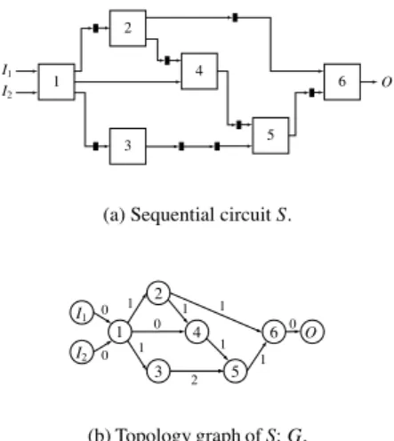
A sequential circuit consists of combinational logic blocks (CLBs) connected with each other directly or through FFs. A CLB in the circuit is a region of connected combi- national logic. The circuit can be modeled by a weighted directed graph defined as follows.
Definition 1 A topology graph for a sequential circuit S is a weighted directed graph G= (V, A, w).
• V is the set of vertices representing primary inputs, pri- mary outputs and CLBs in S.
8th IEEE European Test Workshop, pp.307-312, May 2003.
1
3 4 2
5 6 I1
I2
O
(a) Sequential circuit S.
1 1
1 1
1
2 0
1 0 0
0 I1
I2
1 2
4
3 5
6 O
(b) Topology graph of S: G.
Figure 1. Sequential circuit and its topology graph.
• A Ω V £V is the set of arcs representing FFs and wires in S.
• w : A 7! {0} [ N defines the weights of the arcs, and w(u, v) (u, v 2 V ) denotes the number of FFs on a con- nection(u, v) 2 A, where N is the set of natural num-
bers. 2
Example 1 An example of a sequential circuit and its topol- ogy graph are shown in Figure 1. In Figure 1(a), 1, 2, . . . , 6
are CLBs, and black blocks are FFs. 2
In this paper, we assume that FFs have no hold capa- bility, and those are of D-type. This assumption does not impose restriction on circuit representation because any FF with hold capability or the other types of FFs can be mod- eled by a D-type FF and some logic gates.
2.1 Delay Fault Model
Path Delay Fault Model In a sequential circuit, a path is defined as an ordered set of gates(g0, g1, . . . , gn), where g0is a primary input or an FF and gnis a primary output or an FF, and gate giis an input to gate gi+1(1∑ i ∑ n ° 1). A path has a delay fault if propagation time of rising or falling transition through the path exceeds a specified clock period. Such a delay fault on a path is said to be a path delay fault (PDF)[11]. PDFs can be classified into four categories by the off-input conditions: (1) robust testable, (2) non-robust testable, (3) functional sensitizable and (4) functional un- sensitizable[3, 9]. The robust, non-robust and functional sensitizable PDFs can affect the performance of the circuit, and they are together called functional irredundant faults. Functional unsensitizable PDFs, also called functional re- dundant faults, never independently determine the perfor- mance, and they do not have to be tested. In this paper, in order to simplify the discussion, we do not distinguish (1), (2) and (3).
Definition 2 Let S and p be a sequential circuit and a path in S, respectively. Let f and Sf be the PDF on p and the faulty circuit of S with f , respectively. Let C be the com- binational circuit composed of all the CLBs on p, and let t be a specified clock period of S. In a slow-fast-slow testing1
1In this paper, we assume a slow-fast-slow testing strategy in test ap-
[9], f is testable if there exists an input sequence T for S and Sfsuch that the following conditions hold.
1. By applying an input vector pair(v1, v2) to each input of C, the desired transition is launched at the starting point of p, and the transition is propagated to the end- ing point of p along p. Then, the value induced by v2
at the ending point in Sf is different from that in S at time t.
2. By applying T to Sf,(v1, v2) is justified to each input of C, and the fault effect of f at the ending point is propagated to a primary output.
Such an input sequence T is regarded as a test sequence for
f. 2
Segment Delay Fault Model In a combinational cir- cuit, a segment is defined as an ordered set of gates (g1, g2, . . . , gL), where L is the length of the segment, and gate giis an input to gate gi+1(1∑ i ∑ L ° 1). The length of the segment L can be anywhere from one to the number of gates in the longest path in the circuit. A segment has a delay fault if propagation time of rising or falling transition through the segment exceeds a specified limit. Such a delay fault on a segment is said to be a segment delay fault (SDF) [6]. It is assumed that a segment delay fault is large enough to cause a delay fault on all paths that include the segment. Definition 3 Let C and s be a combinational circuit and a segment in C, respectively. Let f and Cf be the SDF on s and the faulty circuit of C with f , respectively. Let t be a specified limit time. The fault f is testable if there exists an input vector pair(v1, v2) for C and Cfsuch that the following conditions hold.
1. By applying(v1, v2) to the circuits, the desired transi- tion at the starting point of s is launched, and the tran- sition is propagated to the ending point of s along s. Then, the value induced by v2at the ending point in Cf
is different from that in C at time t.
2. The fault effect of f at the ending point is propagated to a primary output by applying(v1, v2) to Cf. Such an input vector pair (v1, v2) is regarded as an two-
pattern testfor f . 2
Notice that it is conceivable that categories of SDFs are the same as those of PDFs.
2.2 Circuit Transformation
In our test generation method, test sequences for path de- lay faults in sequential circuits with DR-structure are gen- erated by applying a combinational ATPG to their time- expansion models [7]. A time-expansion model for an acyclic sequential circuit is defined based on the following time-expansion graph[7].
Definition 4 Let S be an acyclic sequential circuit, and let G= (V, A, w) be the topology graph of S. Let E = (VE, AE,t, l) be a directed graph, where VE is the set of ver- tices, AEis the set of arcs, t is a mapping from VE to the set of integers, and l is a mapping from VEto V . If E satisfies the following four conditions, E is said to be a time-expansion graph (TEG)of G [7].
C1 (CLB preservation) The mapping l is surjective, i.e., 8v 2 V, 9u 2 VEs.t. v= l(u).
plication because a sequential circuit can be considered delay fault-free in both the fault initialization and the fault effect propagation phases.
4
3 I1
I2
1 I1
I2
1 2 2
5
6 O
2
1 3
0 4
Figure 2. Time-expansion graph of G: E.
3
4 2 2
5
6 O
1 I1 I2 1
I1 I2
Figure 3. Time-expansion model of S based on E: CE(S).
C2 (Input preservation) Let u be a vertex in E. For any direct predecessor of u in G, v2 pre(l(u)), there exists a vertex u0in E such that u02 pre(u) and l(u0) = v, where pre(x) is the set of direct predecessors of a vertex x. C3 (Time consistency) For any arc(u, v) 2 AE, there ex-
ists an arc (l(u), l(v)) 2 A such that t(v) ° t(u) = w(l(u), l(v)).
C4 (Time uniqueness) For any vertices u, v 2 VE, if t(u) = t(v) and l(u) = l(v), then the vertices u and v are iden-
tical, i.e., u= v. 2
Example 2 Figure 2 shows the TEG of S (Figure 1(a)). In Figure 2, the character denoted in a vertex is that of the cor- responding vertex in G, and the number located at the top of each column denotes the value of the label of vertices in the column. The graph E satisfies all the conditions in Defini-
tion 4. 2
Note that a TEG of an acyclic sequential circuit is unique if the circuit is a single-output acyclic sequential circuit [7]. Definition 5 Let S be an acyclic sequential circuit, and let G= (V, A, w) be the topology graph of S. Let E = (VE, AE,t, l) be a TEG of G. The combinational circuit CE(S) obtained by the following procedure is said to be the time-expansion model (TEM)of S based on E [7].
1. For each vertex u2 VE, let l(u) 2 V be the CLB corre- sponding to u.
2. For each arc(u, v) 2 AE, connect the output of u to the input of v with a wire in the same way as(l(u), l(v)) 2 A. Note that the connection corresponding to (u, v) has no FF even if the connection corresponding to (l(u), l(v)) has some FFs (i.e., w(l(u), l(v)) 6= 0). 3. In each CLB, lines and logic gates that are reachable to
neither other CLBs nor primary outputs are removed.2 Example 3 Figure 3 shows the TEM of S (Figure 1(a)) based on E (Figure 2). In Figure 3, a highlighted part in a CLB represents a portion of the lines and gates removed
by Step 3 in Definition 5. 2
3 Discontinuous Reconvergence Structure Our test generation method proposed in Section 4 gener- ate a test set for path delay faults in sequential circuits with discontinuous reconvergence structure. We define the struc- ture as follows.
Definition 6 Let G= (V, A, w) be the topology graph of an acyclic sequential circuit S, and let P(u, v) be the set of paths from u to v (u, v 2 V ). Let n(p) (p 2 P(u, v)) be the number of FFs on the path p. The circuit S is said to be a discontinu-
ous reconvergence structure (DR-structure)if it satisfies the following condition.
|n(pi) ° n(pj)| 6= 1 (8u, v 2 V, 8pi, pj2 P(u, v)) 2 Example 4 An acyclic sequential circuit S (Figure 1(a)) sat- isfies Definition 6. Therefore, S is a sequential circuit with
DR-structure. 2
Notice that, from Definition 6, the class of sequential cir- cuits with DR-structure properly includes that of balanced sequential circuits [5, 10].
4 Test Generation
4.1 Test Generation Method
Given a sequential circuit with DR-structure, S, our test generation method proceeds as follows.
For each output cone circuit Scof S, 1. Make a PDF list F of Sc.
2. Construct the topology graph G of Sc. 3. Create the TEG E of G.
4. Construct the TEM CE(Sc) of Scbased on E. For each PDF f2 F,
(a) For CE(Sc), obtain the set of SDFs corresponding to f , and generate a two-pattern test tefor an SDF
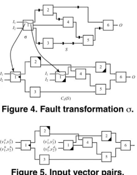
fein the set by using a combinational ATPG2. (b) Transform teinto a test sequence T for f in Sc. (c) Transform T into a test sequence T0for f in S. Note that this test generation scheme can be applied to the other delay fault models, e.g., the transition fault model, etc. Here, we define the fault transformation in Step 4 (a) of the above procedure as follows.
Definition 7 Let S be an acyclic sequential circuit, and let G= (V, A, w) be the topology graph of S. Let E = (VE, AE,t, l) be a TEG of G, and let CE(S) be the TEM of Sbased on E. Let f be the PDF on a path p in S, and let Cbe the combinational circuit composed of all the CLBs on pin S. Let B be the set of the combinational circuits corre- sponding to C in CE(S), and let B0the subset of B whose the input (output) corresponding to the starting (ending) point of p in CE(S) does not removed. A transformation such that B0= µ(C) is said to be the sub-circuit transformation3. Let s in each b02 B0be the segment corresponding to p, and let FE
be the set of SDFs composed of all the s. A transformation such that FE= σ( f ) is said to be the fault transformation4. 2 Example 5 Figure 4 illustrates the fault transformation. In general, a path delay fault in S corresponds to one or more segment delay faults in CE(S). Notice that, from Definition 4, there exists at least one segment delay fault corresponding to a path delay fault even though lines or logic gates in CE(S) are removed by Step 3 in Definition 5. 2 Next, we define the sequence transformation in Step 4 (b) of the above procedure as follows.
Definition 8 Let S be an acyclic sequential circuit, and let G= (V, A, w) be the topology graph of S. Let E = (VE, AE,t, l) be a TEG of G, and let CE(S) be the TEM of Sbased on E. Let tmin be the minimum value of labels as- signed to vertices in E, and let d be the sequential depth of
2If all the SDFs corresponding to f are identified as redundant faults by a combinational ATPG, f is also a redundant fault.
3Transforming b02 B0into C is denoted as µ°1.
4Transforming fe2 FEinto f is denoted as σ°1.
3
4 2 2
5
6 O
1 I1 I2 1
I1 I2
1
3 4 2
5 6 I1
I2
O
S
CE(S ) σ
Figure 4. Fault transformation σ.
3
4 2 2
5 6 1
(v1 1 a,v2
a) (v1
b,v2 b)
(v1 c,v2
c) (v1
d,v2 d)
Figure 5. Input vector pairs.
S. Let Iu= (v1, v2) be an input vector pair to each primary input u2 VEin CE(S). A procedure transforming Iuinto the input pattern to the primary input l(u) 2 V of S at time k (0 ∑ k ∑ d + 1) is said to be the sequence transformation τ. That is, for each u,
Il(u)(k) =
v1 if k= t(u) ° tmin v2 if k= t(u) ° tmin + 1 don0t care otherwise.
Such an input sequence with the length d+ 2 is regarded as
a two-pattern sequence. 2
Example 6 Input vector pairs in Figure 5 are transformed into the two-pattern sequences in Table 1 by the sequence transformation τ. In Table 1, X denotes don0t carevalue. 2 In Step 4 (c) of the test generation procedure, T is trans- formed into T0by applying T to the primary inputs of S cor- responding to the primary inputs of Sc. Note that the other primary inputs of S are assigned don0t carevalues, i.e., each don0t carevalue of T0is placed by 0 or 1.
4.2 Proof of Correctness
In this subsection, we discuss the correctness of our test generation method. In the following discussion, all the proofs of lemmas are omitted due to limitations of space. However, Lemma 1, 2 and 3 can be easily proved from Def- inition 4 and 6, Definition 2 and 4, and Definition 4 and Lemma 1, respectively.
Lemma 1 Let S be a single-output acyclic sequential cir- cuit, and let G= (V, A, w) be the topology graph of S. Let E= (VE, AE,t, l) be the TEG of G. If S is a sequential circuit with DR-structure, S satisfies the following condition.
|t(u) ° t(v)| 6= 1 (8u, v 2 VE s.t. l(u) = l(v)) 2 Lemma 1 guarantees that a two-pattern test te is trans- formed into a test sequence T without conflict of patterns in Step 4 (b) of our test generation method. Notice that, from Lemma 1, if a structure of a sequential circuit is not DR- structure but acyclic structure, conflict of patterns must oc- cur in the sequence transformation. Hence, test generation for such a sequential circuit must be performed by using a sequential path delay ATPG.
Lemma 2 Let SDR be a sequential circuit with DR- structure, and let f be any PDF in SDR. If f is testable, there
Table 1. Two-pattern sequences.
Primary input Time
0 1 2 3 4 5
I1 va1 va2 vc1 vc2 X X I2 vb1 vb2 vd1 vd2 X X
exists a test sequence formed as a two-pattern sequence. 2 Lemma 3 Let SDRbe a single-output sequential circuit with DR-structure, and let G= (V, A, w) be the topology graph of SDR. Let E = (VE, AE,t, l) be the TEG of G, and let CE(SDR) be the TEM of S based on E. Let tmin be the minimum value of labels assigned to vertices in E, and let d be the sequential depth of SDR. Let IC= (v1, v2) be an arbitrary input vector pair to SDR, and let τ(IC) be the two- pattern sequence. Then, the value Ouobserved from a pri- mary output u2 VE by applying v2to CE(SDR) is equal to the value Ol(u)(t(u) ° tmin + 1) observed from the primary output l(u) 2 V at time t(u) ° tmin + 1 by applying τ(IC) to
SDR. 2
From Lemma 1–3, we can have the following theorem. Theorem 1 Let SDR be a single-output sequential circuit with DR-structure, and let G= (V, A, w) be the topology graph of SDR. Let E= (VE, AE,t, l) be the TEG of G, and let CE(SDR) be the TEM of SDRbased on E. Let F be the set of all PDFs in SDR. Then,
1. a PDF f2 F is testable if and only if at least one SDF fe2 σ( f ) is testable, and
2. a two-pattern test for the SDF fe2 σ( f ) can be trans- formed into a test sequence for the PDF f= σ°1( fe). (Proof) Let SDRf be the faulty circuit with f2 F on a path p of SDR, and let CEfe(SDR) be the faulty circuit with fe2 σ( f ) of CE(SDR). Let C be the combinational circuit composed of all the CLBs on p, and let tmin be the minimum value of labels assigned to vertices in E. Let d be the sequential depth of SDR, and let τ°1be the inverse transformation of τ. First, we show that if f is testable, at least one fe2 σ( f ) is also testable. From Lemma 2, there exists a two-pattern sequence Tf if f is testable. From Definition 2, if f is testable, a vector pair(v1, v2) is justified to C at time i and i+ 1 by applying Tf, respectively. Let C0be the combina- tional circuit composed of CLBs such that t(c) = i + tmin in µ(C), where c is a CLB in µ(C). From Definition 4 and Lemma 3, when we apply τ°1(Tf) to CEfe(SDR), (v1, v2) is justified to C0. From Definition 4, since a logic function of the combinational circuit on p with f and that on s with fe
are identical, the value appeared from the ending point of s by applying the 2nd vector of τ°1(Tf) to CEfe(SDR) is equal to the value appeared from the ending point of p at time i+ 1 by applying Tfto SDRf . From the above discussion and Lemma 3, in a slow-fast-slow testing, the value observed from a primary output u2 VE by applying the 2nd vector of τ°1(Tf) to CEfe(SDR) is equal to the value observed from the primary output l(u) 2 V at time t(u) ° tmin + 1 by ap- plying Tf to SDRf . CEfe(SDR) and the TEM CE(SDRf ) of SDRf based on E are isomorphic because feis an SDF on s cor- responding to p. Therefore, the output response of CE(SDRf )
Sequential circuits with acyclic structure
Sequential circuits with DR-structure
Sequential circuits with balanced structure
Figure 6. Classification of sequential circuits by structure.
by applying the 2nd vector of τ°1(Tf) are different from that of CE(SDR) by applying the 2nd vector of τ°1(Tf). Hence, if f is testable, at least one fe2 σ( f ) is also testable.
Next, we show that if feis testable, f= σ°1( fe) is also testable. If feis testable, there exists a two-pattern test tfe. Let s0and Cs0be the segment with feand the combinational circuit composed of all the CLBs on s0, respectively. Let ts0 be the label of CLBs in Cs0, and let(v01, v02) be a vector pair to Cs0. From Definition 4 and Lemma 3, we can justify (v01, v02) to µ°1(Cs0) in SDRf . From Definition 4, since a logic function of the combinational circuit on s0and that on the path p0corresponding to s0are identical, the value appeared from the ending point of s0 by applying the 2nd vector of tfeto CEfe(SDR) is equal to the value appeared from that of p0by applying τ(tfe) to SDRf at time ts0° tmin + 1. From the above discussion and Lemma 3, the value observed from a primary output u02 VE by applying the 2nd vector of tfe
to CEfe(SDR) is equal to the value observed from the primary output l(u0) 2 V at time t(u0)°tmin +1 by applying τ(tfe) to
SDRf in a slow-fast-slow testing. By the same reason as pre- viously, CEfe(SDR) and the TEM CE(SDRf ) of SDRf based on E are isomorphic. Therefore, when τ(tfe) is applied, the output response of SDRand the output response of SDRf are different. Hence, if feis testable, f= σ°1( fe) is also testable.
Finally, from Lemma 1, any two-pattern test for fecan be transformed into a test sequence for f= σ°1( fe) by the sequence transformation τ. Thus, the theorem is proved. 2 From this theorem, we see that our test generation method can not only generate test sequences for all the testable PDFs in sequential circuits with DR-structure, but also identify all the untestable PDFs in the circuits. 5 Advantage of the Test Generation Method 5.1 Characteristics of This Work and Previous
Works
From Definition 6, we can see the relation among acyclic structure, balanced structure and DR-structure shown in Fig- ure 6. In general, a sequential circuit is classified as none of these circuit structures. Therefore, if we generate test se- quences for path delay faults in the sequential circuit by us- ing the method [1], [10] or our method , we need to extract respective circuit structures by using DFT techniques, e.g., partially enhanced scan techniques. In the following discus- sion, we suppose that partially enhanced scan techniques are used to extract respective circuit structures.
Table 2. Comparison of the number of ESFFs.
Circuit
#FF Acyclic structure DR-structure Balanced structure name #ESFF Scan (%) #ESFF Scan (%) #ESFF Scan (%)
s5378 179 30 16.8 92 51.4 106 59.2
Here, we discuss the test generation complexity for each class of sequential circuits and the hardware overhead (the number of ESFFs) required for extracting each structure by partially enhanced scan techniques.
Acyclic structure: The hardware overhead for making a general sequential circuit acyclic is lowest among these three structures. However, given an acyclic sequential cir- cuit, the test generation is more complex than the others because a sequential path delay fault ATPG is required for generating test sequences.
Balanced structure: In the test generation method [10], given a balanced sequential circuit, test sequences for path delay faults in the circuit are generated by applying a com- binational segment delay fault ATPG to its combinationally equivalent circuit. The combinationally equivalent circuit is obtained by just replacing each FF with a wire, and the sizes of the original circuit and the transformed circuit are equal except for FFs. Therefore, the test generation is much easier than the ordinary test generation using a sequential path de- lay fault ATPG. However, the hardware overhead is highest among these three structures.
DR-structure: The hardware overhead is lower than that of balanced structure. Furthermore, we can also generate test sequences for path delay faults in a sequential circuit with DR-structure by applying a combinational segment de- lay fault ATPG to its time-expansion model. Therefore, the test generation can be much easier than the ordinary test generation using a sequential path delay fault ATPG. How- ever, when the circuit is transformed into a time-expansion model, some combinational logic blocks may be duplicated. In worst case, the size of the time-expansion model can be dd/2e times as large as that of the original circuit, where d is the sequential depth of the original circuit. In the next sub- section, we examine the increase rate between the size of a sequential circuit with DR-structure and that of its time- expansion model, and evaluate the effectiveness of our test generation method.
5.2 Case Study
In this case study, we evaluate the effectiveness of the proposed method in the hardware overhead required for ex- tracting DR-structure, the test generation time and the fault efficiency. The following experiment was performed on a Sun Blade 1000 workstation, and we used a combina- tional/sequential delay test generation tool TestGen (Synop- sys) on the workstation. Note that we considered a fault model in test generation as the transition fault model be- cause a combinational ATPG for segment delay faults was not available. However, our test generation method can be applied to fault models which can be tested by two-pattern tests. Therefore, the transition fault model can be also dealt with.
First, we compare the hardware overheads required for extracting acyclic structure, balanced structure and DR- structure from a sequential circuit. We used a circuit, s5378, of the ISCAS ’89 benchmark set. Table 2 shows the hard- ware overheads required for extracting respective structures.
Table 3. Test generation result for s5378: Acyclic structure vs. DR-structure.
Sequential ATPG Combinational ATPG (acyclic structure) (DR-structure) TGT (sec) FE (%) TGT (sec) FE (%)
3721.58 99.07 352.78 100.00
Column “#FF” denotes the number of FFs in the original cir- cuit. Columns “#ESFF” and “Scan (%)” in each column of circuit structure denote the number of ESFFs and the per- centage of ESFFs in each structure, respectively. Note that we obtained s5378 with acyclic structure, SA, by the exact algorithm [2], and s5378 with DR-structure, SDR, and s5378 with balanced structure, SB, were extracted by applying a greedy algorithm to SA. Here, let us explain the greedy al- gorithm for SDR briefly. The greedy algorithm traverse SA from the primary inputs of SA to the primary outputs of SA by a depth-first fashion. In traversing SA, if paths of SAdo not satisfy the condition of Definition 6, an FF on the paths is replaced by an ESFF in order for the paths to satisfy the condition. Thus, we obtained SDRfrom SA. SBwas obtained in a similar way. The time for extracting each structure was negligibly short. In Table 2, “Scan” of SDRwas larger than that of SA. However, “Scan” of SDRwas the value of°7.8% compared to that of SB. Thus, DR-structure can be obtained from a sequential circuit by paying low hardware overhead compared to balanced structure.
Next, we evaluate test generation time and fault effi- ciency for SA and SDR. In our method, test generation was performed for each output cone of SDR, and when a fault was shared by some output cones, we only generated a test sequence for the fault in an output cone, i.e., when the fault was detected in an output cone, we removed the fault from the fault list of SDR. In Table 3, column “Sequential ATPG” denotes the test generation result using a sequential ATPG for SA, and column “Combinational ATPG” denotes the re- sult using a combinational ATPG for the time-expansion model of SDR. Columns “TGT (sec)” and “FE(%)” denote test generation time and fault efficiency under the non-robust criteria for transition faults, respectively. In the output cones of SDR, the maximum percentage of increase between each output cone and its time-expansion model was about +9.1%5. Despite increasing the circuit size, our method achieved 100% fault efficiency with very short test gener- ation time compared to the conventional method using a se- quential ATPG. Thus, our method can significantly improve the test generation time and the fault efficiency by paying large hardware overhead compared to acyclic structure.
We cannot show more results for the other benchmark circuits because part of procedures in the method is still not automated. However, from the above study, we can see that our method is effective in the hardware overhead, the test generation time and the fault efficiency.
6 Conclusions
This paper presented a new structure, called discontin- uous reconvergence structure (DR-structure), of sequential
5The sequential depth of SDRwas four.
circuits with easy testability for path delay faults. We pro- posed a path delay test generation method for sequential cir- cuits with the structure. In our method, instead of a sequen- tial path delay fault test generation algorithm, a combina- tional segment delay fault test generation algorithm is used to generate test sequences for path delay faults. We the- oretically proved the correctness of the proposed method. Our method can be used not only path delay faults, but also the other delay fault models which can be detected by two- pattern tests, e.g., segment delay faults, transition faults, and so on. We confirmed that our test generation method can re- duce test generation time and can enhance fault efficiency compared to the ordinary test generation method using a sequential delay fault test generation algorithm. To apply our method to general sequential circuits, we used a par- tially enhanced scan design to extract DR-structure from the circuits. Theoretically, the class of sequential circuits with DR-structure properly includes that of balanced sequential circuits. Therefore, it is conceivable that the number of en- hanced scan FFs required for extracting DR-structure from a sequential circuit is smaller than that required for extract- ing balanced structure (our previous work [10]). By the case study, we confirmed that the hardware overhead for our method can be reduced compared with that for our previous method.
Acknowledgments The authors would like to thank Michiko Inoue of Nara Institute of Science and Technol- ogy and Tomoo Inoue of Hiroshima City University for their valuable comments.
References
[1] T. J. Chakraborty, V. D. Agrawal and M. L. Bushnell, “Design for testability for path delay faults in sequential circuits,” Proc. 30th ACM/IEEE Design Automation Conf., pp. 453–457, 1993. [2] S. T. Chakradhar, A. Balakrishnan and V. D. Agrawal, “An exact
algorithm for selecting partial scan flip-flops,” Proc. 31st ACM/IEEE Design Automation Conf., pp. 81–86, 1994.
[3] K.-T. Cheng and H.-C. Chen, “Delay testing for non-robust untestable circuits,” Proc. Int. Test Conf., pp. 954–961, Oct. 1993. [4] B. I. Dervisoglu and G. E. Stong, “Design for testability: Using
scanpath techniques for path-delay test and measurement,” Proc. Int. Test Conf., pp. 365–374, 1991.
[5] R. Gupta, R. Gupta and M. A. Breuer, “The BALLAST methodology for structured partial Scan design,” IEEE Trans. on Computers, Vol. 39, No. 4, pp. 538–544, Apr. 1990.
[6] K. Heragu and V. D. Agrawal, “Segment delay faults: A new fault model,” Proc. 14th IEEE VLSI Test Symp., pp. 32–39, 1996. [7] T. Inoue, T. Hosokawa, T. Mihara and H. Fujiwara, “An optimal
time expansion model based on combinational ATPG for RT level circuits,” Proc. 7th Asian Test Symp., pp. 190–197, Dec. 1998. [8] Y. C. Kim, V. D. Agrawal and K. K. Saluja, “Combinational test
generation for various classes of acyclic sequential circuits,” Proc. Int. Test Conf., pp. 1078–1087, Oct. 2001.
[9] A. Krsti´c and K.-T. Cheng, Delay fault testing for VLSI circuits, Boston: Kluwer Academic Publishers, 1998.
[10] S. Ohtake, S. Miwa and H. Fujiwara, “A method of test genera- tion for path delay faults in balanced sequential circuits,” Proc. 20th IEEE VLSI Test Symp., pp. 321–327, May. 2002.
[11] G. L. Smith, “Model for delay faults based upon paths,” Proc. Int. Test Conf., pp. 342–349, Nov. 1985.