A DFT Selection Method for Reducing Test Application Time of System-on-Chips
Masahide Miyazaki1, Toshinori Hosokawa1, Hiroshi Date1, Michiaki Muraoka1, and Hideo Fujiwara2 1 – Design Technology Development Depertment,
Semiconductor Technology Academic Research Center (STARC)
5F Yusen Shin Yokohama Bldg., 3-17-2, Shin Yokohama, Kohokuku, Yokohama 222-0033, Japan 2 – Graduate School of Information Science, Nara Institute of Science and Technology (NAIST),
8916-5 Takayama, Ikoma, Nara 630-0101, Japan
Email:{ miyazaki.m, hosokawa, date, muraoka}@starc.or.jp, [email protected] TEL:+81-45-478-3215 / FAX:+81-45-478-3299
Abstract
This paper proposes an SoC test architecture generation framework. It contains a database which stores the test cost information on several DFTs for every core, and DFT selection part which performs DFT selection for test cost minimization using this database in the early phase of the design flow. Moreover, the DFT selection problem is formulated and the algorithm which solves it is proposed. Experimental results showed that bottlenecks in test application time when using the single DFT method for all cores in a SoC are reduced by performing DFT selection from several DFTs. As a result, the whole test application time is drastically shortened.
keywords: test scheduling, test access mechanism, wrapper, design for test
1. Introduction
With the progress of the semiconductor process technology, the gate count of SoCs are increasing as large as one hundred million gates through the use of 100 nm process design rule toward 2010. As the size of the SoC is getting larger, the reduction of the design productivity will be the most important issue. The technologies that solve this issue are the design reuse methodology and design automation at the high level design phase. Research and development of these technologies is the key to innovate the SoC design methodology.
In order to reduce design time, SoCs consist of a large number of reusable cores. To test such SoCs, a test pattern is prepared for each core, and the modular testing of embedded cores are carried out. Effective modular test requires efficient management of the test resources for core-based SoCs. This involves the design of core test wrappers and TAMs (Test Access Mechanisms), and the scheduling of core tests. In recent years, many research works relevant to these have been presented.
Core test Wrapper design and TAM design are important since they have impact on hardware overhead and test
application time. There are three main approaches to achieve accessibility of embedded cores. The first approach is based on test bus architectures by which the cores are isolated from each other in test mode using a dedicated bus [1][2][3] around the cores to propagate test data. The second approach uses boundary scan architectures [4][5] to isolate the core during test. The third approach uses core bypass mode [6] or transparency [7][8][9]. Wrapper/TAM design include wrapper optimization, core assignment to TAM wires, sizing of the TAMs, and routing of TAM wires. So, Wrapper and TAM co-optimization approach [10] is one of the important subjects.
The objective of test scheduling [11][12][13] is to minimize test application time under one or more of the following constraints: maximum TAM width, maximum allowed power dissipation. Furthermore, optimal wrapper width selection and test scheduling techniques have been proposed [14][15].
Most of the above research works assume scan design as a core's DFT, or do not mention about a core's DFT. To cope with the testing of large and complex SoCs, the modular testing of embedded cores will have to rethink. For the core which is reused in a high level design methodology, the test integrator has to determine the DFT method along with the required quality and cost. For this reason, the technique of determining an SoC test architecture including DFT of each core, taking test cost and test quality into consideration, during the early design phase is needed.
In this paper, we present the DFT selection method for reducing test application time under the following constraints: maximum TAM width, maximum allowed power dissipation, total area size, test data size. The proposed technique does not consider TAM design issue. Each core's DFT is chosen from scan design or non-scan DFT [16][17].
This paper is organized as follows. In section 2, a framework of SoC test architecture generation is proposed. In section 3, the core’s DFT method and the precondition of this research work are described. In section 4, the formulation of the DFT selection problem and the algorithm which solves it are proposed. It is followed by experimental results in section IEEE the 12th Asian Test Symposium (ATS'03), pp.412-417, Nov. 2003.
5. Finally, section 6 concludes this paper.
2. A Framework of SoC Test Architecture Generation
Fig.1 shows our SoC test architecture generation framework. The framework consists of the following stages.
SoC (Gate level, After DFT)
Test Pattern (SoC I/F) Test Pattern (Wrapper I/F) Wrapper
Test Pattern (Core I/F) DFT for each Core
Core (After DFT)
DFT selection Test cost estimation
Test Cost Information
Database
DFT
Wrapper Design ATPG
TAM Design
Test schedule
DFT Selection information SoC
(RTL)
(Synthesis) (a)
(b)
(c)
(d)
(e)
(f)
(g)
(h)
(i)
(j) (1)
(2)
(3)
(4) (5)
SoC (6) (Gate level, After DFT)
Test Pattern (SoC I/F) Test Pattern (Wrapper I/F) Wrapper
Test Pattern (Core I/F) DFT for each Core
Core (After DFT)
DFT selection Test cost estimation
Test Cost Information
Database
DFT
Wrapper Design ATPG
TAM Design
Test schedule
DFT Selection information SoC
(RTL)
(Synthesis) (a)
(b)
(c)
(d)
(e)
(f)
(g)
(h)
(i)
(j) (1)
(2)
(3)
(4) (5)
(6)
Fig.1 Framework (1) Test Cost Estimation
Input: SoC design
Output: Each core’s estimated test cost information for several DFTs
The test cost information on each core is estimated, and the result is output to the test cost information database. In addition, for each core, the test cost information on two or more DFTs are estimated. Test cost information includes the following information.
- Test application time - TAM width - Power dissipation - Area size
- Test data size (2) DFT selection
Input: Test cost information
Output: The selected DFT and correspondent test schedule for each core.
Each core’s DFT selection is optimized to reduce the total test application time, and each core’s selected DFT and test schedule are output.
(3) DFT
Input: The information of each core’s selected DFT, and core design (before DFT)
Output: Core design (after DFT)
According to DFT selection information on each core, design for test of each core is performed.
(4) ATPG
Input: Core design (after DFT) Output: Test pattern (core I/F)
The test pattern of the core is created using existing ATPG tools.
(5) Wrapper Design
Input: Test pattern (core I/F)
Output: Wrapper design, Test pattern (Wrapper I/F) Core test Wrapper is designed in this stage. Based on the test pattern of a core, the bit width compression function is incorporated if needed. Moreover, the test pattern is modified to match the interface of the designed Wrappers.
(6) TAM Design
Input: Top level of the SoC, Core design (after DFT), Wrapper design, test pattern (Wrapper or core I/F), Test schedule
Output: SoC design which includes Wrappers, TAMs, and each core’s DFT
The simultaneously tested cores are divided into several TAMs according to the test schedule, and an SoC design which include TAMs is created. Moreover, the test pattern of each core is edited and output with the interface of SoC pin.
The framework uses the following data or information. (a) SoC (RTL)
RTL described SoC design. (b) Core (After DFT)
Core design (after DFT). (c) Wrapper
Core test wrapper design. The bit width adjustment function is incorporated, if needed.
(d) SoC (Gate level, After DFT)
SoC design which includes Wrappers, TAMs, and each core’s DFT.
(e) Test Cost Information Database
The database where each core’s estimated test cost information for several DFTs are stored.
(f) DFT selection information
Each core’s DFT method which was selected to reduce the total test application time.
(g) Test Schedule
Test start time and test end time of each core. (h) Test Pattern (Core I/F)
Each core’s test pattern. (i) Test Pattern (Wrapper I/F)
The test pattern which is modified to match the interface of the Wrapper.
(j) Test Pattern (SoC I/F)
The test pattern which is modified to match the interface of the SoC pins.
The DFT selection part is especially important among the above mentioned framework. The test integrator determines the SoC’s test strategy, including DFT of each core, taking test cost and test quality into consideration in this early design phase. So, we propose the DFT selection method in section 4 to reduce test cost under the following constraints: maximum TAM width, maximum allowed power dissipation, total area size, and test data size (Fig.2).
1
5 6
4
3 2
ATE memory
Core2:DFT3 Test Cost InformationCore2:DFT2Test Cost
InformationCore2:DFT1Test Cost Information Core1:DFT3 Test Cost InformationCore1:DFT2Test Cost
InformationCore1:DFT1Test Cost Information
:
Core1:DFT1 Test Data Core2:DFT2 Test Data
:
Max Area Size
Max Data Volume
MAX TAM width Max Power
Test Cost Information Database -Power -Area Size -TAM width -Test Data Volume -Test Application Time
Fig.2 DFT selection
3. DFT of Each Core
3.1. Scan Design Method Full scan design is one of the most popular DFT methods. Since output and input test data flow serially through the scan chain, test application time depends on the maximum scan chain length. For this reason, if a large TAM width can be taken, a scan chain can be divided and the maximum scan chain length (Fig.3), and test application time can be shortened.
However, when the number of chains is large, as shown in Fig.3, the scan chain length becomes a stair function. Thus even if TAM width increases, test application time is not always shortened [14].
The preconditions for scan design are as follows.
(1) The number of scan chains shall be chosen in the range of 1 to max (the number of input ports of the core, the number of output ports of the core). However, in the stair function portion shown in Fig.3, only the pareto-optimal-points[14] are adopted.
(2) The frequency of the test clock is assumed to be 1/5 of the system clock of normal operation.This assumption is based on the survey of some product data.
3.2. Non-Scan DFT method
Scan design methods have the following disadvantages concerning test cost and test quality:
- The additional test circuits for DFT cause the degradation of performance.
- The test length is very long. - It is not suited for at-speed-testing.
In order to drastically improve the above-mentioned disadvantages while keeping complete fault efficiency, non-scan DFT methods[16][17] for RTL design circuits were proposed. In this paper, the non-scan DFT method (NS-DFT) of reference [16] shall be chosen as another DFT of a core.
The preconditions for NS-DFT are as follows.
(1) Several Wrappers (Fig.4) with bit width compression function must be prepared, and the choice of TAM width shall be given.
In our implementation, we use the coding technique using EOR network [18][19] for input data compression, and we use EOR tree for the output data compression. In addition, these compression techniques do not change the test length. (2) The frequency of the test clock is the same as the system clock at normal operation.
(Fix value for isolation) F
core
Direct Input
Test Input Functional
Input Wrapper
Mode signal
Test mode
clock Async. reset
Functional Output
Test Output F
F F F
Decoder Encoder
(Fix value for isolation) F
core
Direct Input
Test Input Functional
Input Wrapper
Mode signal
Test mode
clock Async. reset
Functional Output
Test Output F
F F F
Decoder Encoder
Fig.4 Example of Wrapper design for NS-DFT
4. DFT Selection Problem Formulation and Algorithm
4.1 DFT Selection Problem Formulation We formulate the DFT selection problem as follows. Inputs:
(1) Test cost information on each core : D=Dij (wij, pij, vij, aij, tij) Here, wij, pij, vij, aij, tij are, respectively:
wij: TAM width of core i to which DFT j is applied. pij: maximum power consumption of testing core i to
which DFT j is applied.
aij: Area of core i to which DFT j is applied.
vij: The amount of test data of core i to which DFT j is applied.
tij: Test application time of core i to which DFT j is applied.
(2) Maximum TAM width of the SoC : W 1
100
4 10 16 22 28 34
Number of chains
chain length
candidate points
Fig.3 Relationship between scan chain length and number of chain
1 100
4 10 16 22 28 34
Number of chains
chain length
candidate points
1 100
4 10 16 22 28 34
Number of chains
chain length
candidate points
Fig.3 Relationship between scan chain length and number of chain
(3) Maximum available peak power of the SoC: P (4) Maximum amount of the total test data size: V (5) Maximum area of the SoC: A
Outputs:
The information of each core’s selected DFT information and test schedule
Objective:
The test application time of the SoC is minimum, and constraints (Input: (2), (3), (4), (5)) are satisfied.
To solve this problem, an algorithm is proposed in the next paragraph.
4.2 Algorithm
The algorithm is shown in Fig. 5. The following variables are used in this algorithm.
(1) C: Variable to store test cost information on each core: Ci
(DFTi, wi, pi, vi, ai, ti)
DFTi, wi, pi, vi, ai, ti are, respectively: DFTi: DFT of core i.
wi: TAM width of core i. pi: Power consumption of core i. ai: Area of core i.
vi: Test data volume of core i. ti: Test application time of core i.
(2) Cinit: Test cost information under initial DFT selection. (3) Ccurrent: Variable which stores the test cost information under the present DFT selection.
(4) Cbest: Variable which stores the test cost information under DFT selection of the minimum test application time. (5) current_tat: Variable which stores test application time. (6) best_tat: Variable which stores the minimum test application time.
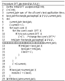
(7) trial_tat: Variable which stores test application time. At the first step, intial DFT selection and the test cost information Cinit are created (line1). Initialize the variable which stores the test cost information current_tat with the sum of the test application time of each core of initial DFT selection (line2).
Next, test scheduling aiming at the formation of the minimum test application time is performed with the rectangle_packaging algorithm[14][15]. The return value of the above-mentioned algorithm is the test application time of the whole SoC. This result is stored in variable best_tat (line4).
Hereafter, while best_tat is updated, change the DFT selection and test scheduling repeatedly (line5-line24). The loop iteration is as follows.
current_tat is updated with the value of best_tat (line6). Test cost information C under the present DFT selection is held as Ccurrent (line7). The following process are performed on all DFTs of each core (line8-line20).
C is updated by the test cost information C’ that DFT was changed about one core (line10 - 11). Test scheduling is performed (line12). Consequently, if the obtained test application time is shorter than best_tat (line13), best_tat w ill be updated (line14) and test cost information C will be stored as Cbest (line15). After all DFTs of the concerned core are tried, C is written back to Ccurrent (line18). Then, after all
core’s trial, if best_tat is updated after trying all cores and all DFTs (line21), Cbest is transposed to C (line22), and go back to the line 6 (line24), otherwise it ends. DFT of each core of Cbest obtained at the end is the solution of DFT selection algorithm.
Procedure DFT_decision(D,W ,P,A,V) 1 Define initialDFT assignm ent Cinit; 2 C =Cinit;
3 current_tat= sum of the all core’s test application tim e; 4 best_tat=Rectangle_packaging(C,W ,P,A,V,current_tat); 5 do{
6 current_tat= best_tat; 7 Ccurrent= C; 8 for(each core ){
9 for( the core’s each DFT ){ 10 if( itis not current DFT ){
11 C=C’; /*change the core’s DFT*/ 12 trial_tat= Rectangle_packaging(C,W ,P,A,V,
current_tat); 13 if( trial_tat < best_tat ){
14 best_tat = trial_tat; 15 Cbest= C;
16 }
17 } 18 }
19 C =Ccurrent; 20 }
21 if( best_tat <current_tat ){ 22 restore C = Cbest; 23 }
24 }W hile(best_tat<current_tat); Procedure DFT_decision(D,W ,P,A,V) 1 Define initialDFT assignm ent Cinit; 2 C =Cinit;
3 current_tat= sum of the all core’s test application tim e; 4 best_tat=Rectangle_packaging(C,W ,P,A,V,current_tat); 5 do{
6 current_tat= best_tat; 7 Ccurrent= C; 8 for(each core ){
9 for( the core’s each DFT ){ 10 if( itis not current DFT ){
11 C=C’; /*change the core’s DFT*/ 12 trial_tat= Rectangle_packaging(C,W ,P,A,V,
current_tat); 13 if( trial_tat < best_tat ){
14 best_tat = trial_tat; 15 Cbest= C;
16 }
17 } 18 }
19 C =Ccurrent; 20 }
21 if( best_tat <current_tat ){ 22 restore C = Cbest; 23 }
24 }W hile(best_tat<current_tat);
Fig.5 DFT selection algorithm 5. Experimental Results
5.1. Experimental Environment
The experimental environment is as follows.
(1) The experiment had been held on the Sun ultra80 workstation, (Sun OS 5.6), 400MHz, 2Gbyte memory. (2) The proposed algorithm was implemented in C. (3) Nine RTL design were used as experimental circuit. (4) To prepare the test cost information, we used the
following conventional EDA tools:
- Power consumption estimation : Wattme / artgraphics
- Logic synthesis : DesignCompiler / Synopsys - Scan path synthesis :DFT Compiler / Synopsys - ATPG : Tetra MAX / Synopsys
- To prepare the test cost information of NS-DFT, we used an inhouse tool.
5.2. Experimental Circuits
Table 1 shows the characteristics of the experimental circuits without DFT. These nine circuits were used as cores. The 1st column shows the core number. The 2nd column shows the number of inputs. The 3rd column shows the number of outputs. The 4th column denotes the number of memory elements. The 5th column shows the area in terms of gate number after logic synthesis. The 6th column shows the estimated power consumption. The power consumption is denoted in the relative values on the basis of the normal operation of core No.1 without DFT. The 7th column denotes
Table 1 Information of the Cores
No. PI bit PO bit # of FF Area power
*1 min - max min - max
1 32 16 51 1094 0.00 1 - 17
2 20 16 192 2525 0.00 1 - 20
3 80 80 228 4494 0.63 1 - 80 32 - 64
4 32 32 83 1647 0.00 1 - 32
5 32 32 115 4713 0.00 1 - 33
6 32 98 1284 40528 0.96 1 - 92 32 - 98
7 58 128 1942 36560 1.25 1 - 122 32 - 128
8 129 260 357 22650 2.55 1 - 179 34 - 260
9 96 224 838 58287 2.20 1 - 210 32 - 224
16 16
32 32 Scan DFT NS-DFT
# of chain TAM width No. PI bit PO bit # of FF Area power
*1 min - max min - max
1 32 16 51 1094 0.00 1 - 17
2 20 16 192 2525 0.00 1 - 20
3 80 80 228 4494 0.63 1 - 80 32 - 64
4 32 32 83 1647 0.00 1 - 32
5 32 32 115 4713 0.00 1 - 33
6 32 98 1284 40528 0.96 1 - 92 32 - 98
7 58 128 1942 36560 1.25 1 - 122 32 - 128
8 129 260 357 22650 2.55 1 - 179 34 - 260
9 96 224 838 58287 2.20 1 - 210 32 - 224
16 16
32 32 Scan DFT NS-DFT
# of chain TAM width
*1 Values relative to the normal operation of core No.1 the minimum number and the maximum number of the scan chains, which were added to prepare test cost information of scan DFT. The 8th column denotes the minimum TAM width and maximum TAM width with which wrappers were designed.
Throughout this experiment, the constraints of the test scheduling were set as follows.
Maximum allowed power dissipation:
(Sum of each core’s power consumption which were denoted in Table 1) * 1.5
Total area size:
(Sum of each core’s area size which were denoted in Table 1) *1.5
Total TAM width: 512, 64 5.3. Experimental Results
We made experiments for the following three cases: (1) Scan only (number of scan chain selection), (2) NS-DFT only (TAM width selection), (3) Scan and NS-DFT (DFT method and number of scan chain, TAM width selection).
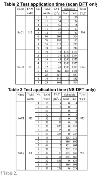
5.3.1. Case 1: Scan only. In case 1, each core’s DFT was limited to scan design. The number of scan chains in each core is selected to reduce the total test application time. Table 2 shows the results of case 1. The 1st column shows the name of SoC. The 2nd column shows each SoC’s maximum TAM width. The 3rd column denotes each core’s number denoted in Table 1. The 4th column shows each core’s selected TAM width. The 5th column shows each core’s test application time. The 6th column and the 7th column shows each core’s test schedule. “Start” denotes each core’s test start time, and “end” denotes each core’s test end time. The 8th column shows each SoC’s total test application time.
In SoC1, a solution for testing all cores simultaneously was obtained. The DFT of core No.6 has the largest test application time among all cores of SoC1, even though the DFT with the smallest test application time was chosen for core No.6. Under this condition, as long as there is no other choice of DFT which improves the test application time of No.6, the total test application time does not improve. In SoC2, the found solution splits the test of core No.6 from the test of all other cores, i.e., core No.6 is tested independently.
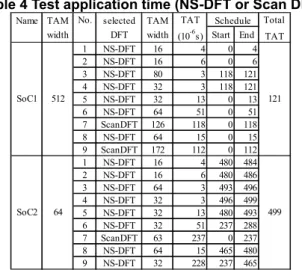
5.3.2. Case 2: NS-DFT only. In case 2, the choice of each core’s DFT was limited to NS-DFT. Table 3 shows the results of case 2. The meaning of each column was the same as that
Table 2 Test application time (scan DFT only)
Name TAM No. TAM TAT Total
width width (10-6s) Start End TAT
1 9 50 0 50
2 11 34 0 34
3 15 56 0 56
4 11 27 0 27
5 12 43 0 43
6 96 304 0 304
7 76 195 0 195
8 55 217 0 217
9 74 244 0 244
1 10 41 1330 1371
2 11 34 1330 1364
3 19 43 1330 1373
4 11 27 1330 1357
5 12 43 1330 1373
6 63 466 864 1330
7 25 657 0 657
8 16 843 0 843
9 23 864 0 864
SoC2 64 1373
304 Schedule
SoC1 512
Table 3 Test application time (NS-DFT only)
Name TAM No. TAM TAT Total
width width (10-6s) Start End TAT
1 16 4 0 4
2 16 6 0 6
3 64 3 0 3
4 32 3 0 3
5 32 13 0 13
6 32 51 0 51
7 32 835 0 835
8 64 15 0 15
9 64 228 0 228
1 16 4 228 232
2 16 6 886 892
3 64 3 901 904
4 32 3 232 235
5 32 13 835 848
6 32 51 835 886
7 32 835 0 835
8 34 15 886 901
9 32 228 0 228
SoC2 64 904
835 Schedule
SoC1 512
of Table 2.
The test application time of core No.7 was very large, and as long as there was no choice of DFT which improves its test application time, the test application time of the whole SoC was not shortened either.
5.3.3. case 3 : Scan and NS-DFT. In case3, each core’s DFT was selected from NS-DFT or scan design. Table 4 shows the result of case 3. The meaning of the 1st-3rd columns is the same as that of Table 2 and Table 3. The 4th column shows the selected DFT. The meaning of the 5-9th columns is the same as that of the 4-8th columns of Table2 and Table 3.
Except for core No.7 and No.9, NS-DFT was chosen by any SoC. The reason of this choice that the test application time of NS-DFT was short, and having chosen the short compared to scan DFT.
As for the test application time of the whole SoC, we obtained the shortest times compared to cases 1 and 2. In case 1, the test application time was longer because of the DFT selected for core No.6. However, in case 3 we could choose another DFT for core No.6 such that test application time improved. In case 2, the test application time was longer because of the DFT select for core No.7. However, in case 3 we could choose another DFT for core No.7 such that test
Table 4 Test application time (NS-DFT or Scan DFT)
Name TAM No. selected TAM TAT Total
width DFT width (10-6s) Start End TAT
1 NS-DFT 16 4 0 4
2 NS-DFT 16 6 0 6
3 NS-DFT 80 3 118 121
4 NS-DFT 32 3 118 121
5 NS-DFT 32 13 0 13
6 NS-DFT 64 51 0 51
7 ScanDFT 126 118 0 118
8 NS-DFT 64 15 0 15
9 ScanDFT 172 112 0 112
1 NS-DFT 16 4 480 484
2 NS-DFT 16 6 480 486
3 NS-DFT 64 3 493 496
4 NS-DFT 32 3 496 499
5 NS-DFT 32 13 480 493
6 NS-DFT 32 51 237 288
7 ScanDFT 63 237 0 237
8 NS-DFT 64 15 465 480
9 NS-DFT 32 228 237 465
SoC2 64 499
121 Schedule
SoC1 512
application time improved.
These experimental results show that the differences in the selection scope of DFT drastically changes the test cost of SoC. Therefore, the usefulness of having a database with the test cost information of several DFTs, and using this database to optimize DFT selection to reduce test cost in early stages of design flow was shown.
6. Conclusions
The framework of a SoC test architecture generation containing a database which stores the test cost information on several DFTs for every core, and DFT selection part which performs DFT selection for test cost minimization using this database in the early phase of the design flow was proposed. Moreover, the DFT selection problem was formulated and the algorithm which solves this was proposed. Experimental results showed that bottlenecks in test application time when using the single DFT method for all cores in a SoC is reduced by performing DFT selection from several DFTs. As a result, the whole test application time is shortened.
Our future work include the following issue. (1) Optimization including the composition of TAM. (2) Add Scan BIST and Non-Scan BIST to the choice of DFT. Acknowledgements
This work was sponsored by NEDO (New Energy and Industrial Technology Development Organization) as VCDS Project (SoC advanced design technology development project). The authors would like to thank Professor Michiko Inoue and Professor Tomokazu Yoneda of Nara Institute of Science and Technology, Professor Tomoo Inoue and Hideyuki Ichihara of Hiroshima City University, and Rafael K. Morizawa of STARC for their valuable discussion and comments.
References
[1]T. Ono, K. Wakui, H. Hikima, Y. Nakamura and M. Yoshida,
“Integrated and automated design-for-testability implementation for cell-based ICs,” in Proc. 6th Asian Test Symposium (ATS’97), pp.
122-125, November 1997.
[2]E. Marinissen, R. Arendsen, G. Bos, H. Dingemanse, M. Lousberg and C. Wouters, “A Structured and Scalable Mechanism for Test Access to Embedded Reusable Cores,” in Proc. International Test Conf., pp. 284-293, October 1998.
[3]P. Vama and S. Bhatia, “A Structured Test Re-Use Methodology for Core-Based System Chips,” in Proc. International Test Conf., pp294-302, October 1998.
[4]N. A. Touba and B. Pouya, “Testing embedded cores using partial isolation rings,” in Proc. VLSI Test Symposium, pp.10-16, May 1997.
[5]L. Whetsel, “An IEEE 1149.1 based test access architecture for ICs with embedded cores,” in Proc. International Test Conf., pp. 69-78, November 1997.
[6]M. Nourani and C. A. Papachristou, “Structural fault testing of embedded cores using pipelining,” J. Electronic Testing: Theory and Applications. vol. 15, pp. 129-144, 1999.
[7]I. Ghosh, S. Dey, N. K. Jha, “A Fast and Low Cost Testing Technique for Core-based System-on-Chip,” in Proc. 35th Design Automation Conf., pp. 542-547, 1998.
[8]I. Ghosh, S. Dey, and N. K. Jha, “A low overhead design for testability and test generation technique for core-based system-on-a-chip,” IEEE Trans.on CAD, vol.18, No.11, pp. 1661-1676, November 1999.
[9]T. Yoneda, H. Fujiwara, “A DFT Method for Core-Based Systems-on-a-Chip Based on Consecutive Testability,” in Proc. 10th Asian Test Symposium (ATS’01), pp. 193-198, November 2001. [10]V. Iyengar, K. Chakrabarty and E. J. Marinissen, “Test Wrapper and Test Access Mechanism Co-Optimization for System-on-Chip,” J. Electronic Testing: Theory and Applications.vol.18, pp. 213-230, April 2002
[11]Y. Huang, W. T. Cheng, C. C. Tsai, and N. Mukherjee, “Resource Allocation and Test Scheduling for Concurrent Test of Core-Based SOC Design,” in Proc. 10th Asian Test Symposium (ATS’01), pp. 265-270, November 2001.
[12]E. Larsson, K. Arvidsson, H. Fujiwara, and Z. Peng, “Integrated Test Scheduling, Test Parallelization and TAM Design,” in Proc. 11th Asian Test Symposium (ATS’02), pp. 397-404, November 2002. [13]H. S. Hsu, J. R. Hung, K. L. Cheng, C. W. Wang, C. T. Huang, and C. W. Wu, “Test Scheduling and Test Access Architecture Optimization for System-on-Chip,” in Proc. 11th Asian Test Symposium (ATS’02), pp. 411-416, November 2002.
[14]V. Iyengar, K. Chakrabarty and E. J. Marinissen, “On using rectangle packaging for SOC wrapper/TAM co-optimization,” in Proc. VLSI Test Symposium, pp. 253-258, May 2002.
[15]Y. Huang, N. Mukherjee, S. Reddy, C. Tsai, W. Cheng, O. Samman, P. Reuter, and Y. Zaidan, “Optimal Core Wrapper Width Selection and SOC Test Scheduling Based On 3-Dimensional Bin Packing Algorithm,” in Proc. International Test Conf., pp. 74-82, October 2002.
[16]H. Date, T. Hosokawa, and M. Muraoka, “A SoC Test Strategy Based on a Non-scan DFT Method,” in Proc. 11th Asian Test Symposium (ATS’02), pp305-310, November 2002.
[17]S. Nagai, S. Ohotake, and H. Fujiwara, “A DFT method for RTL data paths based on strong testability to reduce test application time,” Technical Report of IEICE DC2002-84, pp. 31-36, February 2003.
[18]B. Koneman, “LFSR-Coded Test Patterns for Scan Designs,” in Proc. European Test Conf., pp. 237-242, March 1993.
[19]I. Bayraktarouglu and A. Orailoglu, ”Test Volume and Application Time Reduction Through Scan Chain Concealment,” in Proc. 38th Design Automation Conf., pp. 151-155, June 2001.