Design for Testability Based on Single-Port-Change Delay Testing for Data Paths
Yuki Yoshikawa, Satoshi Ohtake, Michiko Inoue and Hideo Fujiwara Graduate School of Information Science, Nara Institute of Science and Technology
Kansai Science City 630-0192, Japan
Email:{yuuki-y, ohtake, kounoe, fujiwara}@is.naist.jp
Abstract
This paper introduces a new concept of hierarchical testability called Single-Port-Change (SPC) two-pattern testability. We propose a non-scan design-for-testability (DFT) method which makes each path that needs to be tested in a data path SPC two-pattern testable. An SPC two-pattern test guarantees robust (resp. non-robust) test if the path is robust (resp. non-robust) testable. Since it is easy to find justification paths for SPC two-pattern tests at register-transfer level, the proposed DFT method can re- duce hardware overhead compared to that of our previous DFT method for arbitrary two-pattern tests. Furthermore, we propose a method to reduce test generation effort by re- moving a subset of sequentially untestable paths from tar- gets of test generation. Experimental results show that the proposed method can reduce hardware overhead without losing the quality of test.
1. Introduction
The speed of VLSI circuits has accelerated in recent years. High speed VLSI circuits need delay fault testing in order to guarantee the timing correctness of the cir- cuits. There are several delay fault models: path delay fault model, transition fault model, segment fault model, and so on. Among these, path delay fault is more gen- eral and models defects as cumulative propagation delays along circuit paths that exceed an upper limit[1]. To de- tect a path delay fault in a circuit, it is necessary to apply a two-pattern test to the starting points of a target and other related paths. However, it takes a lot of time for general VLSI circuits to generate test sequence for justification of two-pattern tests. Straightforward solutions are scan-based approaches[2, 3, 4]. However, these techniques have the following disadvantages: (i) under-testing problem arises or (ii) complex test generation is needed and/or (iii) area overhead is high. Moreover, test application time is long because of scan-shift operation. To avoid the disadvan- tages, non-scan design-for-testability (DFT) approaches at register-transfer level (RTL) based on hierarchical test gen- eration have been proposed[5, 6]. The advantage of this approach is that the number of primitive elements at RTL is much small compared to that at gate level. Hierarchical test generation consists of two processes, (i) generating test patterns for combinational blocks at gate-level, (ii) justify- ing the patterns from primary inputs (PIs) to appropriate registers and propagating the responses to primary outputs (POs) at RTL. Our previous work[6] defined hierarchical two-pattern testable (HTPT) data path, in which any two- pattern tests can be applied to each combinational block
from PIs and the responses can be observed at POs. They presented a DFT method at RTL to augment a given data path to HTPT data path, which requires lower area over- head and test application time than enhanced scan approach does. However there is room for further improvement in area overhead. Furthermore, there is possibility of over- testing. Over-testing means that untestable faults before DFT can be tested after DFT. As a result, it leads to lower the process yield and judge good circuits as defective ones. Therefore, it is important to reduce area overhead and re- duce over-testing.
Path delay faults in a combinational circuit are gener- ally classified into four classes: robust testable, non-robust testable, functional sensitizable (FS) and functional unsen- sitizable path delay faults[1]. In [8], robust and non-robust testable path delay faults are classified as the same group called singly-testable (ST). In [7, 8], a path delay fault is robust (resp. non-robust) testable if and only if there ex- ists a Single-Input-Change (SIC) robust (resp. non-robust) test for the fault. In this paper, we propose a new concept of testability at RTL called Single-Port-Change (SPC) two- pattern testability based on the concept of SIC at gate-level. A port means an input and an output of primitive elements (e.g. an operational module and a register) at RTL, and it has bit width. At RTL, a number of combinational 1-bit paths between two ports are regarded as a bundled path. We employ the notion of RTL paths[6]. An RTL path is a path passing through only combinational logic, which starts at a PI or a register and ends at a register or a PO. We propose a DFT method which guarantees SPC two-pattern testability to every combinational block at RTL based on hierarchical test generation, which can reduce area overhead compared to the previous DFT method for HTPT. SPC two-pattern tests can guarantee robust (resp. non-robust) test for a path if the path is robust (resp. non-robust) testable and can also detect a subset of FS path delay faults.
We also address the reduction of over-testing. We pro- pose a method to identify RTL paths which never propa- gate a value from the starting register to the ending register within one clock at normal operation. We refer to such path as Control-dependent Untestable Paths (CUPs).
Experimental results show that the proposed method can reduce hardware overhead without losing the quality of test.
2. Target circuit and fault
An RTL design generally consists of controller and data path, and they are connected each other by control signal lines and status signal lines. Our target part is the data path separated from the controller part. Note that we use in- IEEE the 14th Asian Test Symposium (ATS'05), pp. 254-259, Dec. 2005.
formation of control signals from the controller to identify CUPs. All control signals and status signals of the data path are assumed to be directly controllable and directly observable, respectively. A data path consists of hardware elements (e.g. PIs, POs, registers, multiplexers, operational modules, and observation modules) and lines to connect output ports of hardware elements with input ports of oth- ers. There are two types of input ports of a hardware ele- ment: data input ports and control input ports. Each data input port is reachable directly or indirectly from at least one PI. Each control input port is connected with control signal line. Similarly, there are two types of output ports of a hardware element: data output ports and status output ports. Each data output port is reachable directly or indi- rectly to at lease one PO. Each status output port is con- nected with status signal line. An operational module has one or two data input ports, one data output port and at most one status output port, and an observation module has one or two data input ports, one status output port, at most one control input port. We assume that (i) all lines have same bit width. (ii) There is no chaining of operational modules. Note that chaining modules can be regarded as ninput and one output operational module. We relax the second assumption by extending the consideration of two input modules. We target all the path delay faults except for faults on paths which start at control inputs or end at status outputs.
3. SPC two pattern testability 3.1. SPC two-pattern test
In this section, a combinational block which consists of combinational hardware elements on input cone to a regis- ter is considered at RTL. We refer to an RTL path which is a target of testing as on-path. As opposed to on-path, we refer to an RTL path which supports to the propagation of a transition launching at the starting point of an on-path along an on-path as off-path. For the input port of an operational module on on-path, one of the RTL paths passing through the other port can be an off-path (See the left picture of Fig- ure 1). In this paper, we assume that an operational module has one or two input ports and there is no chaining module, hence the number of off-paths is at most one for each on- path. An SPC two-pattern test is a pair of two consecutive vectors which launches transitions at the port correspond- ing to the starting point of the on-path and sets stable two consecutive vectors for the other ports of the combinational block. When SPC two-pattern tests are applied to a com- binational block, the select signal of each MU X is fixed with an on-path or an off-path being selected. [6] showed that while the select signal of a MUX is fixed, propagation of the signals from the selected input to the output is in- dependent of the signals at the other input. Therefore the on-path is testable if SPC two-pattern tests can be applied to starting point of the on-path and the off-path.
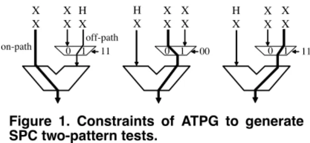
SPC two-pattern tests for combinational blocks can be generated by using a combinational test generation algo- rithm with constraints. To describe the constraints, we use the notation X and H. X denotes that it is possible to gener- ate arbitrary vector and H means that the vector just before is held. In Figure 1, we show an example of constraints for ATPG. X X for an on-path (a bold line in the figure) denotes
X X
H X X X
X X H X
X X
H X
X X
X X
0 1 11 0 1 00 0 1 11
on-path
off-path
Figure 1. Constraints of ATPG to generate SPC two-pattern tests.
that it is possible to generate arbitrary two vectors consecu- tively. X H denotes that the first vector is an arbitrary vector and the second vector is the same as the first one. This is the input constraint for off-path. As we mentioned above, for the inputs other than those on on-path, off-path and the select signal line of each MUX, we do not care generated vectors, hence we denote merely X X .
3.2. Quality of SPC two-pattern test
Smith[7] showed that a path delay fault is testable by a robust test if and only if there exits a robust single-input change (SIC) test for this fault, and Gharaybeh[8] showed that the same applies to non-robust tests. Their theorems show that there exist SIC robust tests for robust testable path delay faults and SIC non-robust tests for non-robust testable path delay faults. At gate level consideration, an SIC two-pattern test launches a transition for 1 bit of inputs of a combinational block, while an SPC two-pattern test can launch transitions for any bits of inputs of the corre- sponding port. Hence SPC two-pattern test can completely cover an SIC two-pattern test. In other words, there exists an SPC robust (resp. non robust) test for a robust (resp. non-robust) testable path delay fault without loss of test quality.
The remaining testable path delay faults are FS path de- lay faults. To test these faults, transitions are needed at multiple inputs. A FS path delay fault which needs transi- tions for some inputs of only on-path can be tested using an SPC two-pattern test. However the fault which needs tran- sitions for some inputs of both on-path and off-path cannot be tested under the concept. By experiments, we examine that how many FS faults become untestable.
3.3. SPC two-pattern testability
We define SPC two-pattern testability for RTL paths. To test an RTL path which does not pass through an opera- tional module with two input ports, one control path and one observation path are sufficient to test the RTL path. Control paths are the paths to justify test patterns from PIs to each register and observation paths are the paths to prop- agate the responses to POs. If we consider only one control path, we need not care about timing conflict to justify test patterns. Timing conflict means that more than or equal to two values are required to the same PI at the same time. Hence it is certainly possible to generate a control path by using a thru function[10], A thru function is added to an operational module in order to propagate a value along a control path or an observation path without changing the value . The realization of a thru function is shown in Sec- tion 5. To test an RTL path p ∈ P which passes through an operational module having two input ports, it is necessary
PI1 PI2 PI
PI
Condition 1 Condition 2
Condition 4 EP1 EP2
EP1 EP2 EPEP11 EPEP22
EP1 EP2 EP1 EP2 C1 C2
: hold resister : resister
PI
Condition 3 EP1 EP2 EP1 EP2 C1’ C2’
Condition 5 EP1 EP2 EP1 EP2
PI
V11
V12
V21
V22
V11
V12
V21
V22
V11
V12 V21
V22
V2 1/2
V11
V12
V11
V12
V21
V22
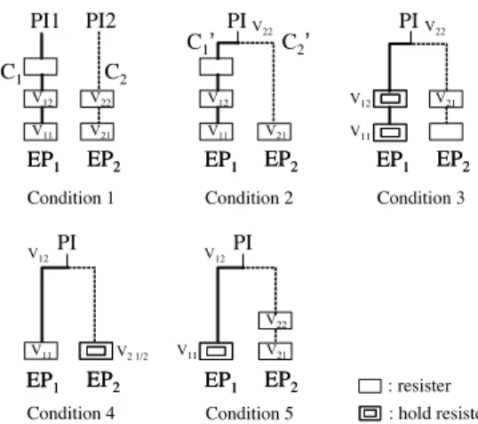
Figure 2. Conditions for C1and C2.
to justify test patterns from a PI or PIs to appropriate reg- isters by a pair of control paths C1,C2 and propagate test responses from an appropriate register to a PO by an ob- servation path Op, where C1 is the path from a PI to the starting register of an on-path p, and C2is the path from a PI to the starting register of an off-path.
Definition 1: An RTL path p is SPC two-pattern testable if there exists a pair of control paths C1and C2that can apply SPC two-pattern tests to the combinational block and Op
that can observe the test responses. 3.3.1. Conditions for control paths
Here, to simplify the following discussion, we assume that there exists a thru function for each input port of every operational module in a data path. In the next section, we will propose an efficient DFT algorithm to add thru func- tion to data paths. In order to support the application of SPC two-pattern tests with a pair of control paths C1 and C2, the difference between the sequential depths of C1and that of C2 and/or the number of hold registers on C1 and that of C2should be considered. The sequential depth of a control path Ciis the number of registers that appear on Ci
and is denoted as SD(Ci). Let EP1and EP2be the ending point of C1and that of C2, respectively. If C1and C2are not disjoint, let C1′and C2′be the paths from the diverging point of C1and C2to EP1and EP2, respectively. In the following theorem, we show necessary and sufficient conditions for a pair of control paths C1and C2to support SPC two-pattern tests.
Theorem 1: A pair of control paths C1and C2 can justify SPC two-pattern tests to their ending points EP1 and EP2
if and only if C1 and C2 satisfy one of the following five conditions.
1. C1and C2are disjoint. 2. |SD(C′1) − SD(C2′)| ≥ 2
3. There exist at least two hold registers on C1′. 4. There exists at least one hold register on C2′.
5. There exists at least one hold register on C′1 and SD(C′2) − SD(C1′) = 1
Examples of these conditions are shown in Figure 2. Proof:An arbitrary SPC two-pattern test(V1,V2) is repre- sented as V1= v11&v21and V2= v12&v22. v11and v12are applied to an on-path. v21and v22are applied to an off-path
and they are the same value.
Sufficiency: Since we assume that there exists a thru func- tion between each input and the output of every operational module, we have only to consider timing conflicts. If C1
and C2satisfy Condition 1, it is obviously possible to jus- tify any SPC two-pattern test from PIs to EP1and EP2(see Condition 1 of Figure 2). With regard to Conditions 2,3,4 and 5, although C1and C2are not disjoint, it is also possible to justify any SPC two-pattern test without a timing con- flict. In Condition 2, we first apply the first and the second partial vectors consecutively to the PI for the control path with higher sequential depth. Then we apply consecutively the remaining two vectors to the same PI. In Condition 3, we first load v11and v12into two hold registers on C1′ and hold the values, secondly we apply consecutively v21 and v22to the PI. In Condition 4, we first load v21into hold reg- ister on C2′ and hold the value. Then we apply v11and v12
consecutively. In Condition 5, we first load v11 into hold register on C′1and hold v11, then we apply v21, v22and v12
consecutively.
Necessity: we assume that two control paths C1and C2do not satisfy any of the above five conditions. Such control paths satisfy all the following properties.
1. C1and C2are not disjoint. 2. |SD(C1′) − SD(C2′)| < 2
3. The number of hold registers on C′1is at most one. 4. There is no hold register on C′2.
5. There is no hold register on C′1if SD(C′2) − SD(C1′) = 1.
All the possible pairs of control paths C1 and C2 that satisfy all the above properties are as follows.
• C1and C2are not disjoint and|SD(C1′) − SD(C2′)| = 1 and there is no hold register on both C′1and C2′.
• C1and C2are not disjoint and|SD(C1′) − SD(C2′)| = 0 and there is no hold register on both C′1and C2′.
• C1and C2 are not disjoint and SD(C1′) − SD(C2′) = 1 and there is only one hold register on C′1.
• C1and C2are not disjoint and|SD(C1′) − SD(C2′)| = 0 and there is only one hold register on C′1.
Any pair of control paths C1and C2described above can not guarantee SPC two-pattern test. Therefore five condi- tions are the only conditions for a pair of control paths C1
and C2to justify SPC two-pattern tests from a PI or PIs to
EP1and EP2. □
Here we consider relaxation of the assumption of the number of input ports of an operational module. The fol- lowing theorem shows the sufficient conditions for an op- erational module with n input ports.
Theorem 2: n control paths support the application of SPC two-pattern tests for an RTL path p if either of the follow- ing conditions is satisfied.
1. Any pair of n control paths are disjoint.
2. With regard to each pair of control paths for off-paths which are not disjoint, the mutually disjoint parts from the diverging point to both ending points cross at least one hold register.
The proof of this theorem is similar to that of Theorem 1. As we mentioned in this subsection, to guarantee SPC two-pattern test, a register with hold function is needed even if the difference between sequential depths of C1and
that of C2 is zero. However to guarantee arbitrary two- pattern test in such case, we need more complex hardware element for DFT.
3.3.2. Conditions for observation paths
To observe a test response, the value captured at the end- ing register of an RTL path have to be propagated to a PO without changing the value. Fortunately, we need not care about timing conflict because only one observation path is sufficient to propagate the value. Hence to guarantee the propagation, it is sufficient to add a thru function to each operational module on the observation path.
4. The conditions to identify CUPs
We can obtain information about state transitions of the controller and control signals from the controller to the data path at each state by analyzing the RTL description of the circuit. By considering the timing of data transfer between registers and the structure of a data path, we identify RTL paths as Control-dependent Untestable paths (CUPs).
Let P be a set of RTL paths in a data path and now we consider whether p ∈ P is CUP or not. Let Rsbe the register which is the starting point of p, and let Rebe the register which is the ending point of p. Let CRs and CRe be load enable signals of registers Rsand Re, respectively. If the load enable signal of a register is equal to ’1’, the register loads a value, otherwise, holds its value. Note that in case the register does not have hold function, we assume that a load enable signal line is connected to the register, and the value of that signal is always ’1’. In case the starting point of p is a PI or the ending point of p is a PO, the PI or the PO is treated as a register with no hold function. Let Miand CMi (1 ≤ i ≤ n) be a MUX on p and its select signal, respectively. When Mi selects the input on p, the value of the select signal is denoted as CMi= pMi. Let Si
and Sj be states of the controller. Si and Sjis said to be consecutive if there exists a direct transition from Sito Sj. Let CMn= (ai,aj) be a select signal pair of consecutive two states.
Definition 2: An RTL path p is control-dependent untestable path (CUP) if either of following two conditions is satisfied for any consecutive two states.
1. CRs= (0, −) ∨CRe= (−, 0) −: don’t care 2. ∨ni=1{CMi̸= (−, pMi)}
Theorem 3: All the gate-level paths corresponding to an RTL path p are non-robust untestable if p is CUP.
proof: For the first condition of Definition 2, Rsdoes not launch a transition at Si, or Redoes not capture the response at Sj. For the second condition, p is not selected at Sj
and this prevents propagation of transitions from Rsto Re. Therefore, p is non-robust untestable. □
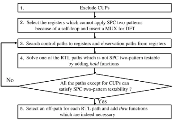
5. DFT method for RTL data path
In this section, we propose a DFT method which makes RTL paths except for CUPs in data paths SPC two-pattern testable.
5.1. DFT element
Additional hardware elements of DFT are multiplexer (MUX), hold function and thru function. We use a MUX to make a new RTL path from a PI to a register. A hold
Exclude CUPs
Select the registers which cannot apply SPC two-patterns because of a self-loop and insert a MUX for DFT
Solve one of the RTL paths which is not SPC two-pattern testable by adding hold functions
Search control paths to registers and observation paths from registers
Select an off-path for each RTL path and add thru functions which are indeed necessary
All the paths except for CUPs can satisfy SPC two-pattern testability ? No
Yes
1.
2.
3.
4.
5.
Figure 3. The flow of our DFT algorithm. function is added to a register for the purpose of holding the value according to need, and it is realized by adding a MUX just before the register to feedback a value from the output to the input. A thru function is explained briefly in Section 4. For a common module, such as adder or mul- tiplier, it is realized by providing a constant value to the other input. It can be provided by adding a mask element. A mask element generates a constant depending on its con- trol signal. For a more complex module or a module with one input port, we cannot realize the thru function by only providing a constant, then we deal with the thru function by bypassing the module using a MUX.
5.2. Algorithm for adding DFT elements
Figure. 3 shows the flow of the proposed DFT algo- rithm.
Step 1: We extract CUPs according to conditions of Theorem 3, and remove them from the consideration for test. Accordingly, not only over-testing is relaxed but it may also be possible to reduce hardware overhead if an RTL path which cannot apply SPC two-pattern tests with- out DFT is judged as CUP.
Step 2: There are some RTL paths which start at a reg- ister and go back to the same register. There are many cases where SPC two-pattern tests cannot be applied to such an RTL path because it is structurally difficult to sat- isfy the conditions of Theorem 1. Since it is only possi- ble to make such an RTL path SPC two-pattern testable by adding MUX (hold function cannot solve this problem) and making a new control path from a PI, we first find such structures. To find RTL paths forming a loop we consider a circuit as a circuit graph consisting of four types of nodes, R, Op, Fo and M, and directed edges. The nodes of type R, Op, Fo and M correspond to a register, an operational module, a fanout and a MUX, respectively, and they are connected by directed edges corresponding to the signal lines of the circuit. We refer to the loop which starts at R-type node and go back to the same node without passing through any other R-type node as a self-loop.
We consider a self-loop. It is impossible to apply SPC two-pattern tests to the RTL path corresponding to the self- loop if there is no M-type node, which can be reached from a PI without passing through the self-loop, between the Op- type node and the R-type node. If one of the RTL paths which starts at Riand passes through Opjis not CUP, the RTL path should be modified into SPC two-pattern testable.
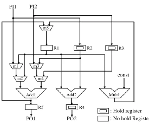
Such an RTL path can be solved by inserting a MUX be- tween Opjand Ri, and adding a new path from a PI to the MUX. Here we consider the self-loop, R1-m1-m2-Add 1- m5-R1 in figure 4 as an example, and corresponding nodes in its circuit graph are named R1,M1,M2,Op1and M5, re- spectively. There is no M-type node between Op1and R1
which can be reached from PI without passing through the self-loop. If one of the RTL paths starting at R1 is not CUP, a MUX is added to the place between Op1and R1then a new RTL path PI1-MUX-R1 is made. When there are some PIs in a circuit, we select the PI such that the pair of control paths is disjoint to satisfy the first condition of Theorem 1. However if there is only one PI in the circuit, we make a new RTL path from the PI. In this case, if the pair of con- trol paths may not satisfy any conditions from second to fifth, hold function is added in Step 4.
Step 3: This step selects candidates for control and ob- servation paths to each register by heuristics. The decision of control and observation paths will be made in step 4.
In order to reduce area overhead and test application time, control paths is selected as they form trees whose source nodes are PIs, accordingly each register is reachable from a PI via a control path with the minimum sequential depth. To search such control paths, we represent the data path as a port graph G= (V, E)[10]. V is the set of all in- put ports and output ports of modules, and E is the set of all directed edges corresponding to the signal lines in the data path and relation between an input and an output of each module (we call the latter edge inside edge). We ap- ply breadth first search (BFS) with respect to the number of registers to the port graph. From the result of the search, we obtain trees which contain the information of control paths with the minimum sequential depth from PIs to regis- ters. The search ends when all the registers become reach- able. In [6][10], to search control paths they also make use of BFS. In this paper, we add a new condition for search which takes advantage of the feature of SPC two-pattern testability. Considering the conditions of Theorem 1, it is desirable that there exists a register with hold on a control path. Therefore we choose a path starting at a hold register if there are some paths which can be chosen at the same sequential depth.
Next we search observation paths with the minimum depth. The search from each register to a PO make use of observation trees. Observation trees are made by per- forming the BFS from each PO on the port graph which is generated by reversing the direction of edges, then we take precedence over the path with control tree if there are some choices, for example, from the output port of an operational module to each input port, to share thru function between control paths and observation paths.
Step 4: For one of the RTL paths which is not SPC two- pattern testable, we modify it into SPC two-pattern testable path by adding a hold function to its starting register. In this step, RTL paths which are not CUPs i.e. the RTL paths need to be tested, and whose pairs of control paths have not yet been determined is dealt with. We first judge RTL paths one by one whether it satisfies one of the conditions of The- orem 1 or not. If the RTL path is SPC two-pattern testable, the pair of control paths generated in Step 3 is determined. However, if the RTL path has no pair of control paths satis-
const
PI1 PI2
PO1 PO2
m1 m2
m3 m4
m5
R1 R2 R3
R4 R5
Add1 Add2 Mult1
: Hold register : No hold Register
Figure 4. LWF benchmark circuit
fying any one of the five conditions at all, it is sufficient to add a hold function to one of the registers which can be the starting points of off-paths in order to satisfy condition 4 of Theorem 1. Among the registers, a hold function is added to the register with the smallest sequential depth. Conse- quently, more control paths share the hold function because a set of control paths forms trees. Here we consider testing of RTL path R2-Add2-R4 in figure 4. The control paths for R2 and R1 are PI1-R2 and PI1-Additional MU X -R1. The additional MUX was already added between m5 and R1 in Step 2. Since the pair of control paths cannot satisfy any conditions of Theorem 1, a hold function is added to R1. If a hold function is added, go back to Step 3 and make the control trees again for the modified circuit. Then only un- solved RTL paths will be target of Step 4 again.
Step 5: We consider how to realize shorter test appli- cation time when there are some choices of off-paths for testing an on-path. We first try to select an off-path having a control path with the minimum sequential depth among them and disjointed from the control path for on-path. If there does not exist such an off-path, that of the minimum depth is selected. We assumed that thru functions are avail- able for all the input ports of all operational modules, how- ever some of them may not be necessary. It is indeed nec- essary to add a thru function between an input port and an output port, corresponding to inside edges on control or observation paths, of an operational module. To realize a thru function, we first search a support path[10] consider- ing timing conflict. A support path is a path from a PI to an input of an operational module, which can justify a con- stant. If there does not exist such a path, we add a mask element or a MUX for bypass to realize it.
6. Experimental Results
In this section, we evaluate the effectiveness of the pro- posed DFT method compared to the previous DFT method for HTPT[6] with regard to area overhead and test applica- tion time. The DFT method which guarantees HTPT data path has similar advantages to enhanced-scan approach and can reduce the area overhead and the test application time. The circuit characteristics of RTL benchmarks used in the experiments are shown in Table 1. Paulin, LWF are widely used circuits. RISC and MPEG are more practi- cal and larger circuits designed by industry. In this exper- iments, we used the logic synthesis tool Design Compiler
Table 1. Circuit characteristics.
Circuit BW #PIs # POs # REGs # RTL path Area
Paulin 16 2 2 7 29 10,550
LWF 16 2 2 5 19 3,322
RISC 32 1 3 40 10,108 94,302
MPEG 8 7 16 241 651 77,554
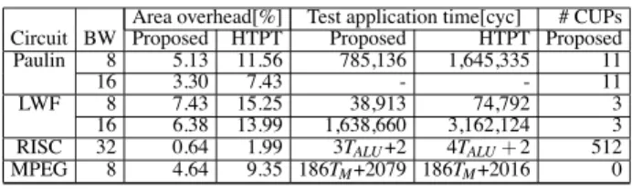
Table 2. Results of DFT and test generation.
Area overhead[%] Test application time[cyc] # CUPs Circuit BW Proposed HTPT Proposed HTPT Proposed
Paulin 8 5.13 11.56 785,136 1,645,335 11
16 3.30 7.43 - - 11
LWF 8 7.43 15.25 38,913 74,792 3
16 6.38 13.99 1,638,660 3,162,124 3
RISC 32 0.64 1.99 3TALU+2 4TALU+ 2 512
MPEG 8 4.64 9.35 186TM+2079 186TM+2016 0
(Synopsys). To generate SPC two-pattern tests, we used the combinational test generation algorithm which supports constraints[11].
Our proposed method guarantees to detect all the faults in a circuit which are detectable in combinational logic blocks separated from the circuit. With regard to robust and non-robust path delay faults the fault coverage of our method is equal to that for HTPT data path if CUPs are not considered. Table 2 shows the results of area overhead, test application time and the number of CUPs. For all bench- mark circuits, area overhead of the proposed DFT method is lower than that of HTPT data path. From the results of Paulin and LWF, the larger the size of circuit, the smaller the area overhead. The difference between area overhead of the proposed method and that of the previous one be- come large if there are many registers which are reached from the same PI and at the same sequential depth. For 8 bit Paulin, 8bit LWF and 16 bit LWF, the proposed method can reduce test application time to about 50% of that for HTPT. The main reason is that the number of target faults can be reduced by removing CUPs. For Paulin and LWF, we judged eleven and three RTL paths as CUPs, respec- tively. The other reason is that previous method adds extra register to these circuits. In such case, extra one cycle is necessary for loading data into such a register. For 16 bit Paulin, RISC and MPEG, it is not practical to test all paths in the data path because the number of paths is extremely large. Therefore we consider the critical parts which affect the difference between test application time of the proposed method and that of previous one. For 16 bit Paulin, a com- binational block composed of two multipliers is the critical part. In the proposed method, many RTL paths through the block are identified as CUPs. However, we cannot es- timate the difference between the number of test patterns for the block in the proposed method and that in the previ- ous method. Hence, we cannot perform symbolic analysis. For RISC, an ALU is critical part and its number of tests is denoted as TALUin the table. The proposed method can re- duce 25% compared to the previous one. For MPEG, a sub circuit composed of 64 identical structures of a chaining module is critical. The number of tests is denoted as TM
in the table. For both methods, the test application times are almost the same. For all circuit except for MPEG, since CUPs are identified, over-testing problem is alleviated.
In subsection 3.2, we showed that SPC two-pattern tests
can test a subset of FS path delay faults. Here, we show that the number of FS path delay faults in three simple op- erational modules which can be tested by SPC two-pattern tests. For a 32 bit adder, there are 1638 FS path delay faults and all the faults can be tested by SPC two-pattern tests. For a 32 bit subtracter, 1042 of the total 1054 FS path de- lay faults are tested. For an 8 bit multiplier, 947 of the total 49328 FS path delay faults are tested. From these results, SPC two-pattern tests do not always test all the FS path de- lay faults of an operational module. If it is necessary to test FS path delay faults of such an operational module which is SPC two-pattern test resistant, we can guarantee applica- tion of arbitrary two-pattern tests by applying our previous DFT method only for the module.
7. Conclusion
This paper proposed a concept of Single-Port-Change (SPC) two-pattern testability and presented an efficient non-scan DFT method for data path. The proposed method can reduce area overhead and test application time com- pared to the previous DFT method for hierarchical two- pattern testability without losing the quality of test. More- over, we alleviated over-testing by removing the control- dependent untestable paths from the consideration of test. Acknowledgements The authors would like to thank Dr. Tomokaze Yoneda and Mr. Virendra Singh (Nara Insti- tute of Science and Technology) for their valuable dis- cussion and their cooperation on this experiment. This work was supported in part by 21st Century COE Pro- gram and in part by Japan Society for the Promotion of Science (JSPS) under Grants-in-Aid for Scientific Re- search B(2)(No. 15300018) and for Young Scientists (B) (No.17700062).
References
[1] Angela Krstic and Kwang-Ting(Tim)Cheng,Delay Fault Testing for VLSI Circuits, Kluwer Academic Publishers, 1998.
[2] J. Savir and S. Patel, “Scan-based transition test,” IEEE Trans. on CAD, Vol. 12, No.8, pp. 1232-1241, Aug. 1993.
[3] J. Savir and S. Patel, “Broad-side delay test,” IEEE Trans. on CAD, Vol. 13, No.8, pp. 1057-1064, Aug. 1994.
[4] B. I. Devadas and G. E. Stong, “Design for testability:Using scan- path techniques for path-delay test and measurement,” Proceeding of International Test Conf, pp. 365-374, 1991.
[5] B. T. Murray and J. P. Hayes, “Hierarchical test generation using pre computed tests for modules,” IEEE Trans. on Computer Aided Design, VOL. 9, NO. 6, pp594-603, Jun. 1990.
[6] Md. Altaf-Ul-Amin, S. Ohtake and H. Fujiwara, “Design for hi- erarchical two-pattern testability of data paths,” IEICE Trans. on Information and Systems, Vol. E85-D, No. 6, pp. 975-984, Jun. 2002.
[7] G. L. Smith, “Model for Delay Faults Based Upon Paths,” Proceed- ing of International Test Conference, pp. 342-349, Nov. 1985. [8] M. A. Gharaybeh, M. L. Bushnell and V. D. Agrawal, “Classifica-
tion and Test Generation for Path-Delay Faults Using Single Stuck- at Fault Tests,” Journal of Electronic Testing:Theory and Applica- tions, Vol. 11, No. 1, pp. 55-67, Aug. 1997.
[9] Wei-Cheng Lai, Angela Krstic, Kwang-Ting(Tim), “On Testing the Path Delay Faults of a Microprocessor Using its Instruction Set,” Proc. 18th VLSI Test Symp., pp. 15-20, 2000.
[10] H. Wada, T. Masuzawa, K. K. Saluja and H. Fujiwara, “Design for strong testability of RTL data paths to provide complete fault efficiency,” Proc. Int. Conf. on VLSI Design, pp. 300-305, 2000. [11] V. Singh, M. Inoue, K. K. Saluja and H. Fujiwara, “Instruction-
based delay fault self-testing of processor cores,” Proc. Interna- tional Conference on VLSI Design 2004, pp. 933-938, Jan. 2004.