On the Non-scan BIST Schemes under Power Constraints for RTL Data Paths
Zhiqiang You Michiko Inoue Hideo Fujiwara Nara Institute of Science and Technology, Ikoma, Nara 630-0192, Japan
{you-z, kounoe, fujiwara}@is.aist-nara.ac.jp
Abstract
This paper proposes three non-scan BIST schemes for RTL data paths and formulates DFT problems for the schemes under power constraints. The proposed schemes include one generic non-scan BIST scheme where we can explore trade-offs among hardware overhead, test application time and power dissipation. We also propose other two schemes, adjacent non-scan BIST scheme and boundary non-scan BIST scheme, as special cases that intend short test application time and low hardware overhead respectively. This paper also presents a power constrained test synthesis and scheduling algorithm for adjacent non-scan BIST scheme intended for short test application time.
1. Introduction
A non-scan built-in self-test (BIST), or test-per-clock BIST, is a promising approach that can realize at-speed testing with low volume test data and thus test application time is short. However, excessive power consumption during BIST application is a considerable problem to be resolved. Moreover, some BIST schemes have high hardware overhead.
The techniques in [1-4] enhance some registers to test registers such as Built-In Logic-Block Observation (BILBO)[5] or concurrent BILBO (CBILBO)[6] so that each module can be tested by test registers connected with
the module directly or only through multiplexers. We call this BIST scheme adjacent non-scan BIST scheme.
Nicolici et al. [3,7] proposed test synthesis and test scheduling algorithm under power constraints for BISTed register-transfer level (RTL) data paths based on adjacent non-scan BIST scheme. Here, test synthesis is the process of allocating test hardware to each module. According to the definitions in [3,7], necessary power dissipation is the power dissipated in tested modules and test registers for them, and useless power dissipation is the power dissipated in untested modules and registers which are not used as test registers. The approach in [3,7] saves power dissipation during applying tests and shifting out of test responses by considering both necessary and useless power dissipation. However, the main objective of this approach is to eliminate useless power dissipation. It may be inefficient to reduce test application time and hardware overhead. In practice, modules also can share test pattern generators (TPGs), i.e., it is possible to test different type modules concurrently. Therefore, we can explore more efficient test synthesis and scheduling algorithm to resolve these problems.
In adjacent non-scan BIST scheme, in order that all the modules can be tested directly or only through multiplexer(s) connected test registers, too many registers are modified to test registers, and hence, hardware overhead is very high.
To achieve low hardware overhead, we previously proposed a BIST scheme for RTL data paths [8-10]. In this scheme, TPGs and response analyzers (RAs) are テ キ ス ト IEEE 4th Workshop on RTL and High Level Testing (WRTLT'03), pp.14-21, Nov. 2003.
placed only at primary inputs (PIs) and primary outputs (POs) respectively, and test patterns and test responses are transferred along paths in the data paths. We call this BIST scheme boundary non-scan BIST scheme. Masuzawa et al. [8] proposed a BIST method for RTL data paths based on single-control testability. The approach in [9] improves the method by introducing concurrent testing in this scheme. The approach in [10] extends the concept of the testability in [8] by introducing time division of TPGs, where different input ports of the same modules can share the same TPG. However, our previous works do not consider power dissipation. Since these methods propagate test patterns and responses through modules in a data path, multiple modules dissipate power to test one module, and may cause high power dissipation. Hence, we need to explore a design for testability (DFT) algorithm also considering power constraints.
In this paper, we propose a more general BIST scheme that covers the above two schemes, adjacent non- scan BIST scheme and boundary non-scan BIST scheme. Generally, TPGs and RAs can be placed not only at the boundary of the data path but also inside of the data path. Any register inside the data path can be a candidate to be augmented to a TPG or an RA. We call this BIST scheme non-scan BIST scheme. A new design for testability and test scheduling algorithm under power constraints need to be investigated. This paper also proposes a power constrained test synthesis and scheduling algorithm for adjacent non-scan BIST scheme. This algorithm remedies the disadvantages as mentioned above. Therefore, it is more efficient to test synthesis and scheduling.
The rest of the paper is organized as follows. The presented problems are formulated in section 2. In section 3, an example to illustrate the formulated problems is given. A power constraints test synthesis and scheduling algorithm is described in section 4. The conclusions are given in section 5.
2. Problem formulation
In this section, we give the definitions of test incompatibility and three BIST schemes. Then, we shall formulate problems to obtain optimum solutions for these schemes.
2.1. Definitions
Before the problem formulations are given, we define three concepts of testability concerned with them. We assume, for simplicity, that each module has exactly two inputs and only one output port.
Definition 1 A data path is adjacent non-scan BIST- able if each module M in the data path can be tested as follows.
There exists a TPG for each input port of M and an RA for the output port of M such that
i. The two input ports do not share a register as TPG. ii. Each port is connected with the corresponding TPG or RA directly or only through multiplexers.
iii. Test patterns generated by the TPGs and test responses of M can be fed into the corresponding input ports and RA concurrently.
Definition 2 A data path is boundary non-scan BIST- able if TPGs and RAs are placed only at PIs and POs respectively, and there exist three paths P1, P2 and P3 for each module M such that
i. P1 and P2 are disjoint or P1 and P2 are intersecting with different sequential depth from the same TPG to the input ports of M.
ii. P1 and P3, P2 and P3 are disjoint.
iii. Each of P1 and P2 is a path from a TPG to an input port of M.
iv. P3 is a path from the output port of M to an RA. v. Any value can be propagated along each of P1, P2
and P3.
Definition 3 A data path is non-scan BIST-able if TPGs and RAs can be placed at PIs and POs respectively, and any register inside the data path can be a candidate to be augmented to a TPG or an RA, and there exist three paths P1, P2 and P3 for each module M such that
i. P1 and P2 are disjoint or P1 and P2 are intersecting with different sequential depth from the same TPG to the input ports of M.
ii. P1 and P3, P2 and P3 are disjoint.
iii. Each of P1 and P2 is a path from a TPG to an input port of M.
iv. P3 is a path from the output port of M to an RA. v. Any value can be propagated along each of P1, P2
and P3.
2.2. Problem formulations
We formulate the following three problems. In the following definitions of three problems, hardware and time are hardware overhead and test application time, respectively. Let fH(hardware, time) be a hardware- intensive cost function as follows.
fH(h1, t1) < fH(h2, t2) if h1 < h2 or (h1=h2 and t1<t2) Similarly, let fT(hardware, time) be a time-intensive cost function as follows.
fT(h1, t1) < fT(h2, t2) if t1 <t2 or (t1=t2 and h1<h2) Problem 1. Design for adjacent non-scan BIST and test scheduling under power constraints
•Input: a data path, and maximum power dissipation limit Pmax.
•Output: an adjacent non-scan BIST-able data path, and test schedule satisfying Pmax.
•Objective:minimizing fT(hardware, time).
In this non-scan BIST scheme, for each module, only registers adjacent to the module can be augmented to TPGs and RAs. BILBO and CBILBO are candidate register architectures to TPGs and RAs. If necessary, a load signal is added for a register. Generally, it dissipates less power to test a module. Therefore, the scheme achieves shortest test application time, but its disadvantage is the highest hardware overhead among the three schemes.
Problem 2. Design for boundary non-scan BIST and test scheduling under power constraints
•Input: a data path, and maximum power dissipation limit Pmax.
•Output: a boundary non-scan BIST-able data path, and test schedule satisfying Pmax.
•Objective:minimizing fH(hardware, time).
In boundary non-scan BIST scheme, TPGs can be placed only at PIs while RAs can be placed only at POs. The additional DFT elements are linear feedback shift registers (LFSRs), multiple-input signature registers (MISRs), multiplexers, load signals for registers, thru- functions and lines. To test a module the test patterns and test responses of the module are transferred along paths in the data paths. Thus, the hardware overhead is lowest and it dissipates most power to test a module while the test application time is highest among the three cases.
Problem 3. Design for the non-scan BIST and test scheduling under power constraints
•Input: a data path, co-optimization ratio α (0≤ α≤1), and maximum power dissipation limit Pmax.
•Output: a non-BIST-able data path, and test schedule satisfying Pmax.
•Objective:minimizing
time hardware+ − ⋅
⋅ (1 α)
α (1)
In non-scan BIST scheme, TPGs and RAs can be placed not only at the boundary of the data path but also inside of the data path, i.e., like boundary non-scan BIST scheme where TPGs and RAs can be placed at PIs and POs respectively and like adjacent non-scan BIST scheme where any registers inside the data path can be enhanced to BILBOs or CBILBOs. We can see that Problems 1 and 2 are special cases of Problem 3. The additional DFT elements are BILBOs, CBILBOs, LFSRs, MISRs, multiplexers, load signals for registers, thru-functions and lines. The hardware overhead, power dissipation for a module and test application time for this case is between the above two cases.
We are doing research on finding an effective method for each problem. Here, we shall only focus on the first adjacent testable methodology.
3. An example of the formulated problems
In this section we will present an example to illustrate the formulated problems. The following example shows trade-offs between test application time and hardware overhead among these three BIST schemes.
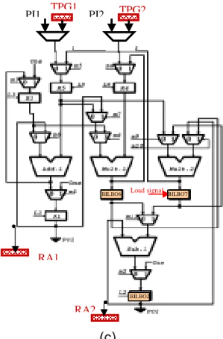
TPG1 TPG2
PI1 PI2
BILBO5 BILBO4
Load signal
BILBO6 BILBO7
Example 1 We consider three BIST schemes for a benchmark circuit, Paulin. Here, we consider testing four modules Add.1, Mult.1, Mult.2 and Sub.1. Like [3,7] we assume that the test length for adders, subtracters and multipliers are T+ =T-= Tu and T* = 4Tu, the test length for the modules which have one of three type paths [10] are Ttype2=1.5Ttype1 and Ttype3=2Ttype1; The power dissipation for registers, BILBO, CBILBO, adders, subtracters, multipliers and multiplexers are assumed to be PREG = PBILBO=P+ =P-=Pu, PCBILBO=2Pu, P* = 4Pu, PMUX=0.2Pu. The peak power constraint is assumed to be Pmax=17.5 Pu.
If we resolve this example using adjacent non-scan BIST scheme the registers R4, R5, R6 and R7 can be enhanced to BILBOs and R1, R2 can be enhanced to CBILBOs (Figure 1(a)). CBILBO1 and BILBO5 can generate test patterns for Add.1 and CBILBO1 analyses its test response. The test registers of modules Mult.1, Mult.2 and Sub.1 are {BILBO5, BILBO4, BILBO6}, {BILBO5, BILBO6, BILBO7} and {BILBO7, CBILBO2} separately. The power dissipation is equal to 13.2Pu and 17.2 Pu for
BILBO6 BILBO7
RA1
CBILBO1
CBILBO2
(a)
TPG1
RA1
RA2
PI1 PI2 TPG2
Load signal
thru thru thru
thru
(b)
RA2
BILBO2
(c)
Figure 1. Data path example (a). adjacent non-scan BIST scheme; (b). boundary non-scan BISTscheme; (c). non-scan BIST scheme.
{Add.1, Sub.1} and {Mult.1, Mult.2} separately. Therefore, we can schedule the test under given peak power constraint by two test sessions {{Add.1, Sub.1}, {Mult.1, Mult.2}}. The test length is equal to 5Tu.
If we use boundary non-scan BIST scheme, it only need to add four thru-functions, and add a load signal for register R7 (Figure 1(b)). The module Add.1 can be test by test registers TPG1 and RA1 and choosing type 3 path while the module Sub.1 can be test by test registers TPG2 and RA2 and choosing type 3 path through the right port of Mult.1. The modules Mult.1 and Mult.2 both use TPG1, TPG2 and RA2 to test. The power dissipation is equal to 16.8Pu, 15.4Pu and 16.2Pu for {Add.1, Sub.1}, {Mult.1} and {Mult.2} separately. Therefore, the test schedule under given peak power constraint is {{Add.1, Sub.1}, {Mult.1}, {Mult.2},}. The test length equals to 10Tu.
However, if we use non-scan BIST scheme, we enhance registers R2, R6 and R7 to BILBOs and add a load signal for register R7 (Figure 1(c)). The module Add.1 can be test by test registers TPG1 and RA1 and choosing type 3 path while the module Sub.1 can be test by test registers BILBO6 and RA2 and choosing type 3 path. The test registers of module Mult.1 and Mult.2 are {TPG1, TPG2, BILBO6} and {TPG1, BILBO2, BILBO7} separately. The power dissipation is equal to 16.8Pu and 16.4Pu for {Add.1, Sub.1} and {Mult.1, Mult.2} separately. By considering power dissipation the test schedule is {{Add.1, Sub.1}, {Mult.1, Mult.2}}. The test length is equal to 6Tu.
It notes that the last two BIST schemes also can test multiplexers which cannot be completely tested using the first BIST scheme. It makes them have more potential to get higher fault coverage. To simplify and achieve comparability we only give an example by test the function modules of the data path.
4. Power constraints test synthesis and scheduling algorithm
This section proposes a power constrained test synthesis and scheduling algorithm for RTL data paths of adjacent non-scan BIST scheme.
4.1. Overview of the algorithm
This subsection gives an overview of the algorithm. More details of this algorithm are showed in the following subsections.
This algorithm consists of the two stages, test synthesis and test scheduling. In the test synthesis, we allocate test registers for all modules as TPGs or RAs. To describe the algorithm, first we define test incompatibility as follows.
Definition 4 Two modules are incompatible, i.e. they cannot be tested simultaneously, if they have one of the following conditions.
i. One module uses a register as LFSR while the other module uses the same register as MISR.
ii. Both modules use the same register as MISR. The algorithm repeats stage1 and stage 2 until all modules are scheduled.
Stage 1. Test synthesis. In this stage, we try to allocate test registers for all modules to lower area overhead and increase test compatibility to achieve shorter test application time.
1. Allocate tentative TPGs for all unscheduled modules.
2. Allocate tentative RA for each unscheduled module if possible.
Stage 2. Test scheduling. In this stage, we schedule one test session by following steps.
1. Get the test incompatibility graph
2. Schedule a test session by using test incompatible graph
3. Refine the result 4. Update the data path.
4.2. Allocate tentative TPGs for all unscheduled modules
To reduce hardware overhead and increase test compatibility between modules, we try to minimize the number of test registers assigned as TPGs. Let RSETj be a set of input ports of modules with which a register Rj is connected directly or only through multiplexer(s). This minimization problem is equivalent to the minimum set cover problem to find the minimum set R of registers such that covers all the unscheduled modules.
However, this problem is NP-complete, therefore, we propose a heuristic algorithm.
U
R R
j j
RSET
∈
First, we select some mandatory registers as follows. If an input port of a unscheduled module in connected with only one register, we select the register. Then, we select registers one by one from the reigeter Rj whose RSETj includes the most uncovered input ports. To lower hardware overhead, it is necessary to reuse the registers which have been test registers in previous test sessions. We select the register which is modified to test register rather than other registers when all of them connect the most undecided input ports directly or only through multiplexer(s).
4.3. Allocate tentative RA for each unscheduled module
In this step, we try to allocate as many RAs as possible for modules under the condition that the modules can be tested in one test session. One module needs only one register as a RA, and one register can be a RA for one module. We reduce this problem into the following the maximum weighted matching problem.
The Hungarian algorithm [11] is used to resolve this problem. The input to the algorithm is a weighted bipartite graph described below. Let G=(V, E) be the complete bipartite graph with vertex set V=M∪R, where M={M1, M2,… , Mn} is the set of modules and R={R1, R2,… , Rk} is the set of registers which can be modified as RAs for modules. A weight function is defined as follows.
w(i, j)=l-R(j), if there is a direct connection or a connection only through multiplexer(s) from Mi to Rj.
=-1, otherwise.
Where R(j) is the number of unscheduled modules that Rj is TPG for; l is a large enough natural number so that l is great than all R(j).
If there is a direct connection or a connection only through multiplexer(s) from Mi to Rj, R(j) also implies the number of incompatible modules with Mi. Thus the maximal weighted matching means the minimum incompatibility. In another word, the aim of this step is to enhance test compatibility to achieve shorter test application time.
4.4. Get the test incompatibility graph
We get the incompatibility graph from the results of the last step, where node set consists of the unscheduled modules and edges exists only between incompatible modules.
4.5. Schedule a test session by using test incompatible graph
Before presenting this step a concept is necessary to definite. For modules can share TPGs, the power dissipation in LFSRs need not be counted for all modules under test.
Definition 5. Essential power dissipation: only the power dissipated in the tested module and its MISR are essential power dissipation.
In this step, we shall select a set of modules that are tested in one test session under power constraint. We extend the scheduling algorithm [12] that obtains a test scheduling under power constraint from a given incompatibility graph. The approach in [12] schedules modules based on necessary power dissipation. We extend it to consider useless power dissipation as well as essential power dissipation.
4.6. Refine the result
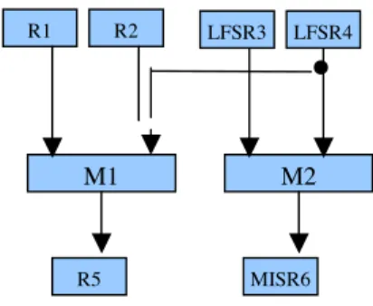
Now, we have obtained a set of modules scheduled in one test session, where TPGs and RA are assigned to each module in the session. We refine the assignment keeping compatibility of the modules in the test session. An example is given to illustrate how to refine the assignment. We consider Figure 2 as an example, where R2 is assigned to an input of M1 as a TPG. If R2 has not been modified as a TPG but R4 has been modified, we can reduce hardware overhead by reassign R4 to the input port in of M. We repeat such refinement until we fail to reduce hardware overhead and useless dissipation. Finally, if the peak power dissipation is decreased, we try to add module(s) in the test session using left edge algorithm under peak power constraint.
We do the following sub steps keeping compatibility of the modules in the test session. First, if possible, we change another register as RA for each module in the test session one by one. If the change makes to decrease hardware overhead or useless power dissipation then accept, else reject. Then, being similar as last sub step, if possible, we change another register as TPG for the input ports which can share a register as TPG until all input ports of modules in the test session are considered. If the change makes to decrease hardware overhead or useless power dissipation then accept, else reject. Finally, if the peak power dissipation is decreased, we try to add module(s) in the test session using left edge algorithm under peak power constraint.
4.7. Update the data path
In this step, we denote the scheduled modules by
“scheduled” and modify each register which is used in the test session as test register to BILBO or CBILBO.
5. Conclusions
This paper proposed three non-scan BIST schemes for RTL data paths and formulated DFT problems for the schemes under power constraints. The proposed schemes include one generic non-scan BIST scheme where we can explore trade-offs among hardware overhead, test application time and power dissipation. We also proposed other two schemes, adjacent non-scan BIST scheme and boundary non-scan BIST scheme, as special cases that intend low hardware overhead and short test application time respectively. This paper also presented a power constrained test synthesis and scheduling algorithm for adjacent non-scan BIST scheme intended for short test application time. Experimental results will be given to demonstrate the performance and practicality of our new approach. We are also still going on the research on finding an effective method for Problems 2 and 3.
LFSR3
R1 R2 LFSR4
M1 M2
R5 MISR6
Figure 2. Reassign test registers. Acknowledgement
This work was supported in part by Japan Society for the Promotion of Science (JSPS) under Grants-in-Aid for Scientific Research No. 14658092.
References
[1] M.S. Abadir and M.A. Breuer, “A knowledge based system for designing testable VLSI chips,” IEEE Design and Test of Computers, vol. 3, pp. 56-68, Aug. 1985.
[2] S. Lin, C. Njinda and M. Breuer, “Generating a family of testable designs using the BILBO methodology,” Journal of Electronic Testing: Theory and Applications (JETTA), vol. 4, no. 1, pp. 71–89, 1993.
[3] N. Nicolici and B. M. Al-Hashimi, Power-Constrained
Testing of VLSI Circuits. Kluwer Academic Publishers, Boston, MA, 2003.
[4] N. Nicolici and B. Al-Hashimi, “Efficient BIST hardware insertion with low test application time for synthesized data paths,” in Proc. IEEE/ACM Design Automation and Test in Europe (DATE 99), pp. 289-295, March 1999.
[5] B. Koenemann, J. Mucha and G. Zwiehoff, “Built-in logic block observation techniques,” in Proc. Int’l. Test Conf. (ITC’79), pp. 37-41, October, 1979.
[6] L.T. Wang and E.J. McCluskey, “Concurrent Built-in logic block observer (CBILBO),” in Proc. The Int. symp. On Circuits and systems, pp. 1054-1057, 1986.
[7] N. Nicolici and B. Al-Hashimi, “Power Conscious Test Synthesis and Scheduling for BIST RTL Data Paths,” in Proc. Int’l Test Conf. (ITC’2000), pp. 662-671, 2000.
[8] T. Masuzawa, M. Izutsu, H. Wada and H. Fujiwara, “Single- control testability of RTL data paths for BIST,” in Proc. 9th Asian Test Symposium. (ATS’2000), pp. 210-215, 2000. [9] K. Yamaguchi, H. Wada, T. Masuzawa and H. Fujiwara, “A BIST Method Based on Concurrent Single-Control Testability of RTL data paths,” in Proc. 10th Asian Test Symposium. (ATS’2001), pp. 313-318, 2001.
[10] K. Yamaguchi, M. Inoue and H. Fujiwara, “Hierarchical BIST: Test-Per-Clock BIST with Low Overhead,” Digest of papers 3rd Int’l Workshop on RTL and High Level Testing. (WRTLT’2002), pp. 42-47, 2002.
[11] D. Jungnickel, Graphs, Networks and algorithms, Springer- Verlag, Berlin, 1999.
[12] V. Muresan, X. Wang, V. Muresan and M. Vladutiu, “The left edge algorithm and the tree growing technique in block-test scheduling under power constraints,” in Proc. of the 18th IEEE VLSI Test Symposium (VTS’2000), pp. 417-422, 2000.