学位論文 博士 工学
GaN HEMT を用いた宇宙環境耐性
優 小型軽量高効率 次世代宇宙用
電力増幅回路 関す 研究
2013 年度
総合研究大学院大学物理科学研究科
宇宙科学専攻
小林 雄太
i
目
第 1 章 序論 ... 15
1 1 研究背景 ... 16
1 1 1 宇 通信 現状 課題 ... 16
1 1 2 化 物半 体[1-3] ... 19
1 2 本研究 目的 意義 ... 23
1 3 本論文 構成 ... 24
1 4 文献 ... 24
第 2 章 効率宇 用電力増幅回路 実現 向 ... 25
2 1 TWTA 同等 効率 持 SSPA 実現 向 設計目標 ... 26
2 2 関連研究 本研究 置付 本研究 解決 課題 ... 28
2 3 文献 ... 32
第 3 章 GaN HEMT 用い 宇 用電力増幅回路設計 ... 36
3 1 設計手法 ... 37
3 2 遥 ... 38
3 2 1 搭載用 考慮 目 ... 38
3 2 2 X帯搭載用 遥 手法 ... 40
3 3 出力 RF DC特性 得 ... 42
3 4 X帯搭載用 非線形 構築 ... 45
3 5 効率電力増幅回路設計 ... 50
3 6 文献 ... 56
第 4 章 GaN HEMT 用い 宇 用電力増幅回路作製 評価 ... 57
4 1 搭載用 考慮 実装方法 用い 宇 用電力増幅回路作製 ... 58
4 2 宇 用電力増幅回路評価 ... 65
4 2 1 基本性能評価 ... 65
4 2 2 動作点 特性 改善 ... 70
4 2 3 X帯20W級SSPA 評価 ... 75
4 3 信 確度設計 向 確 推 非線形 調 ... 77
4 4 ... 84
4 5 文献 ... 85
第 5 章 宇 環境耐性評価 ... 86
5 1 評価 目 ... 87
5 2 X帯搭載用 遥 手法 評価 ... 87
5 2 1 放射線試験 ... 87
5 2 2 熱真空試験 ... 93
5 3 搭載用 考慮 実装方法 評価 ... 100
5 4 課題 検討 ... 105
ii
5 5 文献 ... 107
第 6 章 結論 ... 108
謝辞
... 112論文
... 114iii List of Tables
Table 1-1 Comparison between TWTA and SSPA by merit and demerit. ... 18 Table 1-2 Comparison of semiconductor devices of Si, GaAs, GaN and 4H-SiC by lattice
constant, band gap, relative permittivity, breakdown electric field, saturation electron velocity, thermal conductivity, electron mobility and Johnson’s figure or merit. ... 21 Table 2-1 Comparison of existing X-band onboard PAs by specifications, such as PA type,
output power, size, weight, power consumption, PAE and total efficiency. ... 27 Table 2-2 Target specifications of space-use amplifier for next generation SSPA
comparable to TWTA with respect to RF output power, linear Gain, PAE, radiation tolerance, operation temperature and vacuum condition. ... 28 Table 3-1 Comparison between S-band terrestrial application and X-band space
application of GaN HEMTs by type, matching, structure and substrate. ... 41 Table 3-2 Parameter description of Angelov nonlinear GaAs FET model. ... 47 Table 4-1 Comparison of thermal conductivity of (a) solder paste includeing
Sn-3.0Ag-0.5Cu, Au-20Sn, Sn-37Pb and Ag paste, and (b) base plate (case) including Cu, CuMo and Al. ... 61 Table 4-2 Density, thermal conductivity and heat capacity of the materials (Cu, CuMo, Al,
Au-20Sn, Sn-3.0Ag-0.5Cu, AD1000, GaN and SiC) used in thermal analysis ... 64 Table 4-3 Comparison of Gain, P1dB, P3dB, the maximum output power (Pmax), the
maximum power added efficiency (PAE Max) with respect to the X-band, 20-W, space-use amplifier using GaN HEMT (TGF2023-05) between measurement data and simulation (design) data under the condition of operation frequency at 8.4 GHz, 8.425 GHz and 8.45 GHz. ... 68 Table 4-4 Comparison of the maximum output power (Pmax) and the maximum power
added efficiency (PAE Max) with respect to the X-band, 20-W, space-use amplifier using GaN HEMT (TGF2023-05) between Vg=-3.4 V, Vg=-3.6 V and Vg=-3.8 V under the condition of operation frequency at 8.4 GHz and Vd=28 V. ... 72 Table 4-5 Comparison of the maximum output power (Pmax) and the maximum power
added efficiency (PAE Max) with respect to the X-band, 20-W, space-use amplifier using GaN HEMT (TGF2023-05) between Vd=26 V, Vd=28 V and Vd=30 V under the condition of operation frequency at 8.4 GHz and Vg=-3.5 V. ... 73 Table 4-6 Comparison of the maximum output power (Pmax) and the maximum power
added efficiency (PAE Max) with respect to the X-band, 20-W, space-use amplifier using GaN HEMT (TGF2023-05) between operation frequency at 8.4 GHz, 8.425 GHz and 8.45 GHz with Vd=30 V and Vg=-3.8 V. ... 74 Table 4-7 Comparison of RF output power, linear Gain and power added effieicncy (PAE)
with respect to the RF unit of X-band 20 W-class SSPA including the amplifier using GaN HEMT (TGF2023-05) between target value and measurement data. ... 76
iv
Table 4-8 Size, weight, output power, power consumption and efficiency of X-band 20 W-class SSPA including the amplifier using GaN HEMT (TGF2023-05). ... 76 Table 4-9 Comparison of output power, power consumption and total efficiency between
the existing X-band onboard amplifiers and X-band 20 W-class SSPA including the amplifier using GaN HEMT (TGF2023-05). ... 76 Table 4-10 Comparison of parameters with respect to the constructed GaN HEMT
(TGF2023-05) nonlinear model between design-time value and adjusted value. ... 81 Table 4-11 Comparison of the minimum value of S11 (S11 Min), the maximum value of
S21 (S21 Max), the minimum vlue of S22 (S22 Min) and the frequency of each data with respect to the X-band, 20-W, space-use amplifier using GaN HEMT (TGF2023-05) between measurement data, design-time simulation data and adjusted simulation data under the condition of Vd=28 V and Idset=0.5 A. ... 82 Table 4-12 Comparison of Gain, P1dB, P3dB, the maximum output power (Pmax), the
maximum power added efficiency (PAE Max) with respect to the X-band, 20-W, space-use amplifier using GaN HEMT (TGF2023-05) between measurement data, design-time simulation data and adjusted simulation data under the condition of operation frequency at 8.4 GHz. ... 83 Table 5-1 Comparison of power added efficiency (PAE), output power (Pout), input power
(Pin) and Gain with respect to GaN HEMTs (F344, TGI7785-25L and NPT25015) between radition start time and radiation finish time. ... 89 Table 5-2 Comparison of the degradation of output power (Pout) and power added
efficiency (PAE) between GaN on SiC HEMTs (F344 and TGI7785-25L) and GaN on Si HEMT (NPT25015) at the time of both after total ionizing dose (TID) test and after accelerated aging test. ... 90 Table 5-3 Comparison of the differences of output power (Pout) and power added
efficiency (PAE) between GaN on SiC HEMTs (F344 and TGI7785-25L) and GaN on Si HEMT (NPT25015) at the conditions of both high and low temperature in thermal vacuum test. ... 94 Table 5-4 Conditions of space environmental test with respect to an X-band 20 W-class
SSPA including the amplifier using GaN HEMT (TGF2023-05), (a) radiation and thermal vacuum, (b) vibration (sine wave), (c) vibration (random wave) and (d) quasi-static acceleration. ... 102 Table 5-5 Comparison of output power, power consumption and total efficiency of an
X-band 20 W-class SSPA including the amplifier using GaN HEMT (TGF2023-05) between after thermal vacuum test, after vibration (sine) test, after vibration (random) test, after shock acceleration test and after radiation test. ... 104
v
List of Figures
Fig. 1-1 Power consumption list of Venus climate orbiter (PLANET-C) by components when an observing program is conducted. ... 16 Fig. 1-2 Appearance and structure of onboard power amplifiers, (a) TWTA and (b) SSPA. ... 18 Fig. 1-3 Categories of semiconductor devices by strucuture, constituent element’s group
and the number of elements. ... 20 Fig. 1-4 Application examples of composite semiconductor devices with respect to both
electronic and light devices. ... 21 Fig. 1-5 Comparison between X-band GaAs HEMT and GaN HEMT whose output powers
are the same by size, drain voltage and drain current. ... 22 Fig. 2-1 Research results of S-band amplifier using GaN by efficiency and output power
in recent 5 years. ... 29 Fig. 2-2 Research results of X-band amplifier using GaN by efficiency and output power
in recent 5 years. ... 29 Fig. 2-3 Comparison between this research and the existing researches with respect to
amplifier using GaN HEMT by how to improve RF characteristics and how to achieve space applicability. ... 31 Fig. 3-1 Flow chart of proposed method with respect to the realization of high-efficiency
and space-use amplifiers. ... 37 Fig. 3-2 S-band amplifiers for earth station, (a) 200-W amplifier, (b) 1-kW amplifier. ... 41 Fig. 3-3 Measurement system specifications of GaN HEMT’s RF and DC characteristics,
(a) measurement circuits and equipments and (b) block diagram. ... 43 Fig. 3-4 (a) magnitude and (b) phase of S-parameters versus operation frequency under
the condition of Vd=28 V and Idset=0.5 A as measurement RF characteristics of GaN HEMT (TGF2023-05). S11 and S22 show the reflection characteristics at input and output ports. S21 means the transmittion characteristics from input port to output port. ... 44 Fig. 3-5 Drain current (Id) versus drain voltage (Vd) when gate voltage (Vg) is swept from
-4.0 V to 0.0 V as measurement DC characteristcs of GaN HEMT (TGF2023-05). ... 45 Fig. 3-6 Equivalent circuit of Angelov nonlinear GaAs FET model. ... 46 Fig. 3-7 (a) magnitude and (b) phase of S-parameters versus operation frequency with
respect to the GaN HEMT device (TGF2023-05) by comparing measurement data (solid line) and simulation data based on the constructed nonlinear model (dotted line) under the condition of Vd=28 V and Idset=0.5 A. ... 48 Fig. 3-8 (a) real part and (b) imaginary part of Y-parameters versus operation frequency
with respect to the GaN HEMT device (TGF2023-05) by comparing measurement data (solid line) and simulation data based on the constructed nonlinear model (dotted line)
vi
under the condition of Vd=28 V and Idset=0.5 A. Y11, Y22 and Y21 show the admittance parameters. ... 49 Fig. 3-9 Drain current (Id) versus drain voltage (Vd) with respect to the GaN HEMT
device (TGF2023-05) by comparing measurement data (solid line) and simulation data based on the constructed nonlinear model (dotted line) under the condition where gate voltage (Vg) is swept from -4.0 V to 0.0 V. ... 50 Fig. 3-10 Basic amplifier circuit structure constructed from RF input port, RF output port,
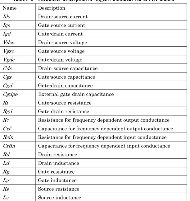
input matching circuit, output matching circuit, gate bias circuit, drain bias cirtuit, GaN HEMT and DC cut capacitors. ... 51 Fig. 3-11 Specific circuit structure of (a) schematic and (b) layout with respect to designed
X-band, 20-W, space-use amplifier using GaN HEMT (TGF2023-05). In (a) schematic, L, W and D mean length [mm], width [mm] and degree of the angle [deg] about each microstrip line components. In (b) layout, blue square shows capacitor, and green square shows resistance. ... 53 Fig. 3-12 Magnitude of S-parameters versus operation frequency with respect to the
designed X-band, 20-W, space-use amplifier using GaN HEMT (TGF2023-05) under the condition of Vd=28 V and Idset=0.5 A. ... 54 Fig. 3-13 Output power (Pout), Gain and power added efficiency (PAE) versus input
power (Pin) with respect to the designed X-band, 20-W, space-use amplifier using GaN HEMT (TGF2023-05) under the condition of operation frequency at 8.4 GHz. ... 54 Fig. 3-14 Stability factors (K and D factors) versus operation frequency with respect to
the designed X-band, 20-W, space-use amplifier using GaN HEMT (TGF2023-05). ... 55 Fig. 3-15 Current distribution with respect to the designed X-band, 20-W, space-use
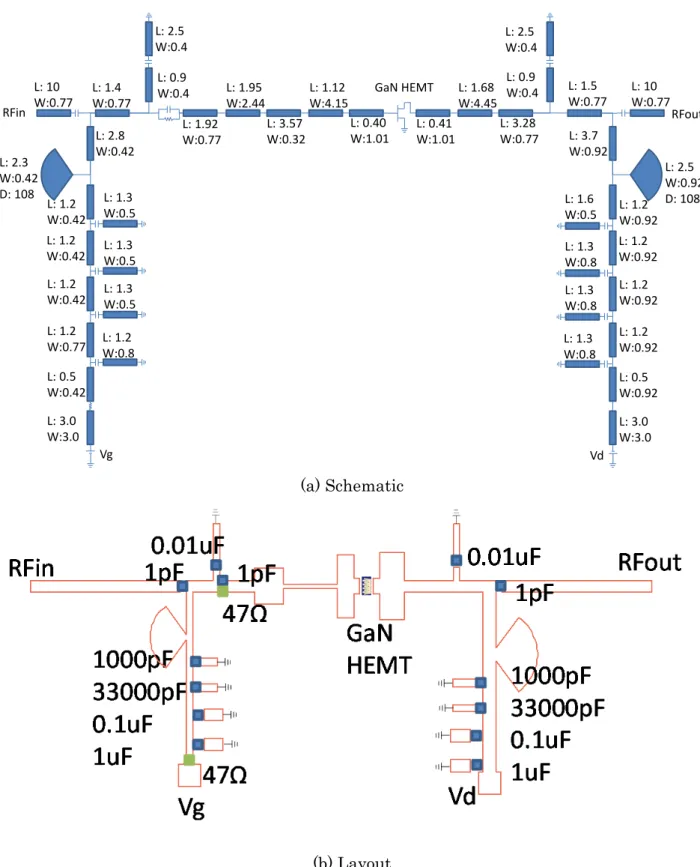
amplifier using GaN HEMT (TGF2023-05) based on electromagnetic analysis under the condition of operation frequency at 8.4 GHz. The color bar means current density per unit of line width [A/m]. ... 55 Fig. 4-1 Appearance of the X-band, 20-W, space-use amplifier using GaN HEMT
(TGF2023-05). RF in and RF out mean input and output port of RF signal. Vg and Vd show gate voltage supply and drain voltage supply ports. ... 58 Fig. 4-2 Detailed picture of the proposed space applicable mounting method of GaN
HEMT device in the X-band, 20-W, space-use amplifier using GaN HEMT (TGF2023-05). ... 59 Fig. 4-3 Comparison of mounting methods by cross-section view between mounting
method using through hole, subcarrier and proposed space applicable method. ... 61 Fig. 4-4 Comparison of mounting methods by thermal analysis between mounting
method using through hole, subcarrier and proposed space applicable method under the assumption that GaN on SiC HEMT is 20-W heat source. ... 64 Fig. 4-5 Block diagram of measurement systems, (a) small signal characteristics, (b)
input-output characteristics and (c) phase noise characteristics. In each figure, DUT
vii
means device undere tested, CPL means coupler, ISO means isolator and ATT means attenuator. ... 66 Fig. 4-6 Magnitude of S-parameters versus operation frequency with respect to the
X-band, 20-W, space-use amplifier using GaN HEMT (TGF2023-05) by comparing measurement data (solid line) and simulation (design) data (dotted line) under the condition of Vd=28 V and Idset=0.5 A. ... 67 Fig. 4-7 Output power (Pout), Gain and power added efficiency (PAE) versus input power
(Pin) with respect to the X-band, 20-W, space-use amplifier using GaN HEMT (TGF2023-05), (a) under the condition of operation frequency at 8.4 GHz (solid line), 8.425 GHz (broken line) and 8.45 GHz (dotted line), and (b) by comparing measurement data (solid line) and simulation (design) data (dotted line) under the condition of operation frequency at 8.4 GHz. ... 68 Fig. 4-8 Measurement results of input power (Pin), output power (Pout), Gain, drain
current (Id) and power added efficiency (PAE) versus time with respect to the X-band, 20-W, space-use amplifier using GaN HEMT (TGF2023-05) under the condition of operation frequency at 8.425 GHz and continuous 300-hour operation time. ... 69 Fig. 4-9 Measurement result of phase noise versus offset frequency with respect to the
X-band, 20-W, space-use amplifier using GaN HEMT (TGF2023-05) by comparing the characteristics of signal source (solid line) and output of the amplifier using GaN HEMT (dotted line). ... 69 Fig. 4-10 Output power versus power added efficiency (PAE) with respect to research
results of X-band amplifier using GaN by comparing this work and recent research concerning CW operation. ... 70 Fig. 4-11 Measurement drain current (Id) versus drain voltage (Vd) with respect to the
GaN HEMT device (TGF2023-05) (a) under the condition where Vd is swept from 0.0 V to 31.8 V and Vg is swept from -4.0 V to 0.0 V as an overall view, (b) under the condition where Vd is swept from 25.0 V to 31.0 V and Vg is swept from -3.8 V to -3.4 V as a specific view. In figure (b), black dot indicates the basic operation point (Vd=28 V and Idset=0.5 A), and red dots show the operation points for evaluation. ... 71 Fig. 4-12 Output power (Pout), Gain and power added efficiency (PAE) versus input
power (Pin) with respect to the X-band, 20-W, space-use amplifier using GaN HEMT (TGF2023-05) by comparing Vg=-3.4 V (solid line), Vg=-3.6 V (broken line) and Vg=-3.8 V (dotted line) under the condition of operation frequency at 8.4 GHz and Vd=28 V. ... 72 Fig. 4-13 Output power (Pout), Gain and power added efficiency (PAE) versus input
power (Pin) with respect to the X-band, 20-W, space-use amplifier using GaN HEMT (TGF2023-05) by comparing Vd=26 V (solid line), Vd=28 V (broken line) and Vd=30 V (dotted line) under the condition of operation frequency at 8.4 GHz and Vg=-3.5 V. .. 73 Fig. 4-14 Output power (Pout), Gain and power added efficiency (PAE) versus input
viii
power (Pin) with respect to the X-band, 20-W, space-use amplifier using GaN HEMT (TGF2023-05) under the condition of operation frequency at 8.4 GHz (solid line), 8.425 GHz (broken line) and 8.45 GHz (dotted line) with Vd=30 V and Vg=-3.8 V. ... 74 Fig. 4-15 Appearance of X-band 20 W-class SSPA including the amplifier using GaN
HEMT (TGF2023-05). ... 75 Fig. 4-16 Flow chart of proposed method with respect to the realization of high-accuracy
design. ... 77 Fig. 4-17 Magnitude of S21 versus operation frequency with respect to the X-band, 20-W,
space-use amplifier using GaN HEMT (TGF2023-05) by comparing measurement data (solid line), simulation (design) data (broken line) and electromagnetic analysis data (dotted line) under the condition of Vd=28 V and Idset=0.5 A. ... 78 Fig. 4-18 Comparison of mounting gate wire length of GaN HEMT (TGF2023-05) by short,
medium and long. ... 79 Fig. 4-19 Magnitude of S21 versus operation frequency with respect to the X-band, 20-W,
space-use amplifier using GaN HEMT (TGF2023-05) by comparing simulation (design) data (broken line), measurement data with short wire (solid grean line), measurement data with medium wire (solid blue line) and measurement data with long wire (solid red line) under the condition of Vd=28 V and Idset=0.5 A. ... 79 Fig. 4-20 Magnitude of S21 versus operation frequency with respect to the X-band, 20-W,
space-use amplifier using GaN HEMT (TGF2023-05) by comparing measurement data (solid line), design-time simulation data (broken line) and adjusted simulation data (dotted line) under the condition of Vd=28 V and Idset=0.5 A. ... 81 Fig. 4-21 Magnitude of S-parameters versus operation frequency with respect to the
X-band, 20-W, space-use amplifier using GaN HEMT (TGF2023-05) by comparing measurement data (solid line) and adjusted simulation data (dotted line) under the condition of Vd=28 V and Idset=0.5 A. ... 82 Fig. 4-22 Output power (Pout), Gain and power added efficiency (PAE) versus input
power (Pin) with respect to the X-band, 20-W, space-use amplifier using GaN HEMT (TGF2023-05) by comparing measurement data (solid line), design-time simulation data (broken line) and adjusted simulation data (dotted line) under the condition of operation frequency at 8.4 GHz. ... 83 Fig. 5-1 Block diagram of measurement system in radiation test. DUT means device
undere tested, CPL means coupler, ISO means isolator and ATT means attenuator. The components in irradiation chamber except for DUT are protected by lead blocks. ... 89 Fig. 5-2 Input power (Pin), output power (Pout), Gain, power added efficiency (PAE) and
drain current (Id) with respect to F344 (X-band GaN on SiC HEMT) versus time and total ionizing dose (TID) during TID exposure under the condition of operation frequency at 8.45 GHz with Vd=24 V and Idset=1.0 A. ... 90
ix
Fig. 5-3 Input power (Pin), output power (Pout), Gain, power added efficiency (PAE) and drain current (Id) with respect to TGI7785-25L (X-band GaN on SiC HEMT) versus time and total ionizing dose (TID) during TID exposure under the condition of operation frequency at 8.45 GHz with Vd=24 V and Idset=1.4 A. ... 91 Fig. 5-4 Input power (Pin), output power (Pout), Gain, power added efficiency (PAE) and
drain current (Id) with respect to NPT25015 (S-band GaN on Si HEMT) versus time and total ionizing dose (TID) during TID exposure under the condition of operation frequency at 2.25 GHz with Vd=28 V and Idset=0.2 A. ... 92 Fig. 5-5 Block diagram of measurement system in thermal vacuum test. DUT means
device undere tested, CPL means coupler, ISO means isolator and ATT means attenuator. ... 94 Fig. 5-6 RF characteristics of F344 in thermal vacuum test, (a) output power (Pout), Gain and power added efficiency (PAE) versus input power (Pin) by comparing under the condition of 25 degC, 1.1E-3 Pa (solid line), 60 degC, 1.2E-3 Pa (broken line) and -20 degC, 5.0E-4 Pa (dotted line) with the operation frequency at 8.45 GHz, Vd=24 V and Idset=1.0 A, (b) output power (Pout), Gain, power added efficiency (PAE), chamber temperature and case temperature of both high and low temperature conditions versus time during thermal vacuum test under the condition of operation frequency at 8.45 GHz. ... 96 Fig. 5-7 RF characteristics of TGI7785-25L in thermal vacuum test, (a) output power
(Pout), Gain and power added efficiency (PAE) versus input power (Pin) by comparing under the condition of 25 degC, 7.9E-4 Pa (solid line), 60 degC, 1.1E-3 Pa (broken line) and -20 degC, 1.5E-3 Pa (dotted line) with the operation frequency at 8.45 GHz, Vd=24 V and Idset=1.4 A, (b) output power (Pout), Gain, power added efficiency (PAE), chamber temperature and case temperature of both high and low temperature conditions versus time during thermal vacuum test under the condition of operation frequency at 8.45 GHz. ... 98 Fig. 5-8 RF characteristics of NPT25015 in thermal vacuum test, (a) output power (Pout),
Gain and power added efficiency (PAE) versus input power (Pin) by comparing under the condition of 25 degC, 1.7E-3 Pa (solid line), 60 degC, 1.3E-3 Pa (broken line) and -20 degC, 5.2E-4 Pa (dotted line) with the operation frequency at 2.25 GHz, Vd=28 V and Idset=0.2 A, (b) output power (Pout), Gain, power added efficiency (PAE), chamber temperature and case temperature of both high and low temperature conditions versus time during thermal vacuum test under the condition of operation frequency at 2.25 GHz. ... 100 Fig. 5-9 Block diagram of measurement system in temperature test. DUT means device
undere tested, CPL means coupler, ISO means isolator and ATT means attenuator. ... 101 Fig. 5-10 Output power (Pout), Gain, power added efficiency (PAE), case temperature and
x
base plate temperature of the X-band, 20-W, space-use amplifier using GaN HEMT (TGF2023-05) versus time during high temperature test under the condition of operation frequency at 8.45 GHz. ... 101 Fig. 5-11 Shock acceleration versus frequency as a condition of space environmental test
with respect to X-band 20 W-class SSPA including the amplifier using GaN HEMT (TGF2023-05). ... 103 Fig. 5-12 HPA case temperature, base plate temperature and vacuum of the X-band 20
W-class SSPA including the amplifier using GaN HEMT (TGF2023-05) versus time during thermal vacuum test under the condition of operation frequency at 8.45 GHz. ... 103 Fig. 5-13 Achievement in this research and expected future plan. ... 106
xi
Nomenclature
f Frequency Hz
λ Wave length M
Vd Drain voltage V
Vg Gate voltage V
Id Drain current A
Idset Drain current at operation point A
Ig Gate current A
Pin Input power dBm
Pout Output power dBm
Gain Gain dB
PAE Power Added Efficiency %
IM3 3rd order inter modulation dBc
P1dB 1 dB compression point dBm
P3dB 3 dB compression point dBm
S11 Reflection characteristics at port 1 - S22 Reflection characteristics at port 2 - S21 Transmission characteristics from port 1 to port 2 - S12 Transmittion characteristics from port 2 to port 1 - Y11 Short-circuit admittance parameter (I1/V1) - Y22 Short-circuit admittance parameter (I2/V2) - Y21 Short-circuit admittance parameter (I2/V1) - Y12 Short-circuit admittance parameter (I1/V2) -
TID Total Ionizing Dose krad
xii Abstract
One of the most indispensable impacts on onboard power consumption has been generally caused by a transmitting power amplifier among the other spacecraft bus subsystems. Due to the large amount of power consumption, it is inevitable that the size (or footprint) and weight of the transmitting power amplifiers become large for heat release. Therefore, developing a highly-efficient onboard transmitting power amplifier is one of the great issues for future various space missions. From these backgrounds, this research concerns the world’s first space-use amplifier circuit using a gallium nitride (GaN) high-electron mobility transistor (HEMT) for the realization of space-tolerant, small-sized, lightweight, and highly-efficient onboard transmitting power amplifier.
Regarding onboard transmitting power amplifiers, travelling-wave tube amplifier (TWTA) and solid-state power amplifier (SSPA) have been mainly used. In general, TWTA uses a vacuum tube called traveling-wave tube and its component total efficiency is up to 35 to 55%. In contrast, SSPA usually uses a gallium arsenide (GaAs) based field-effect transistor (FET) and its total efficiency is around 20 to 30%. Due to the highly-efficient characteristics, TWTA has been mainly used as a high power amplifier dealing with more than 20-W output power. However, with respect to mechanical environment tolerance, lifetime, occupied area (footprint), and discharge risk, SSPA is superior to TWTA because TWTA uses a fragile sculpted-glass tube and needs high voltage (kV) operation. Thus, highly-efficient SSPA has been strongly required and a highly-efficient amplifier circuit is quite important to achieve this. In this research, GaN is selected as an amplification device among the other semiconductor devices since it has the characteristics of high breakdown voltage and high thermal conductivity in addition to wide band gap. As a result, in comparing Johnson’s figure of merit, the suitability as high power and high frequency device, GaN is up to about 100 times higher than GaAs. In addition, GaN is expected to handle large RF power in small size with high efficiency compared to GaAs since GaN’s current density in HEMT structure is larger than that of GaAs as well as breakdown voltage and thermal conductivity of GaN is superior to those of GaAs. Here, researches concern amplifier using GaN have been reported a lot. However, they mainly focus on the realization of high power, high frequency and high efficiency. In other words, how to apply GaN to amplifier circuits for space applications has never proposed. Therefore, this research focuses on the following to achieve this:
I: Device selection method of X-band GaN HEMT for space-use amplifier.
II: X-band, highly-efficient, highly-reliable and highly-accurate amplifier design/evaluation method that can minimize the error between design and measurement in order to enhance the reliability for space applications as well as achieve high efficiency.
III: Mounting method of GaN HEMT considering harsh space environment.
With respect to the device selection of X-band GaN HEMT for space-use amplifier, it requires completely different attitude from the selection of S-band, terrestrial GaN HEMT. This is because that there are so many highly-efficient, internally-matched and packaged GaN HEMTs in S-band, but no such devices in X-band. In addition, realizing high power in parallel structure using low power devices and operating with active
xiii
thermal control system can be done only for terrestrial applications since there are no strict restrictions regarding size, weight and heat release environment. Considering these things, this research selects externally-matched and bare-chip GaN HEMT that can deal with high power in single-end structure. Moreover, GaN on silicon carbide (SiC) HEMT is selected so as to enhance the space applicability since SiC has good material properties such as high thermal conductivity and wide band gap compared to silicon (Si). To evaluate the validity of the device selection method, X-band GaN on SiC HEMT and S-band GaN on Si HEMT are tested by thermal vacuum and radiation (total ionizing dose). There are no specific differences between X-band GaN on SiC HEMT and S-band GaN on Si HEMT in thermal vacuum test whose temperature range is from -20 to 60 degC. However, in total ionizing dose test using 60Co, S-band GaN on Si HEMT is degraded up to 1.37 dB of output power and 21.7% of PAE after 320-krad exposure even though X-band GaN on SiC HEMT is not affected at all. Therefore, it is confirmed that proposed device selection method of X-band GaN HEMT is feasible for space-use amplifier.
Next, the realization of X-band, highly-efficient, highly-reliable and highly-accurate amplifier design and evaluation method is one of the great issues for space applications. At the beginning, we conduct both small signal and large signal design using the nonlinear device model that is constructed based on Angelov GaAs FET nonlinear model and the model parameters are modified for GaN HEMT on the basis of measurement RF and DC characteristics. In this case, although fabricated amplifier demonstrates superior (highly-efficient) performance such as 10.1 dB of small signal gain, 42.6 dBm of maximum output power and 47.3% of maximum PAE at 8.4 GHz, the errors between design and measurement are not enough small to enhance the reliability for space applications. For instance, the error of small signal gain is 2.2 dB, peak frequency is 129 MHz, the maximum power at 8.4 GHz is 0.3 dB and the maximum PAE at 8.4 GHz is 4.4%. To reduce these errors, we propose to estimate the error of bonding wire between model and measurement by modifying the length of bonding wire in measurement since the model behavior of bonding wire in circuit simulator is uncertain although it has a profound effect on the peak frequency in measurement. Here, in general, the errors due to the uncertainties of bonding wire are tried to reduce by adjusting the fabricated circuit patterns, such as adding or cutting the copper substrate by trial and error since modifying the length of bonding wire in measurement is quite difficult. However, this kind of method leads to a considerable change in the fabricated circuit patterns. As a result, it becomes extremely-difficult to evaluate the differences between design and measurement fairly as well as to achieve highly-reliable and highly-accurate design and evaluation. By contrast, since proposed estimation can remove the uncertainties of bonding wire without any adjustment of the fabricated circuit patterns, we can fairly estimate the differences between design and measurement. Therefore, it is possible that the remaining errors due to the uncertainties such as parasitic capacitance or parasitic inductance caused by mounting are estimated by adjusting parameters with respect to drain, gate and source capacitances and inductances in the nonlinear model. Consequently, the error of small signal gain becomes 0.5 dB, peak frequency becomes 18 MHz, the maximum power at 8.4 GHz becomes 0.2 dB and the maximum PAE at 8.4 GHz becomes 1.2%. As observed above, we achieve X-band, highly-efficient, highly-reliable and highly-accurate amplifier design and evaluation method for space applications by constructing a nonlinear model in order to conduct a certain level of highly-accurate design and make it possible to adjust the model parameters, estimating the uncertainties in measurement without
xiv
any adjustment of the fabricated circuit patterns and adjusting the parameters in the constructed nonlinear model.
Finally, a mounting method considering harsh space environment is quite important since high-power and continuous-wave (CW) operation without any active thermal control is required in space applications as well as heat release characteristics is demanded to be free of the influence of space environment such as vibration, shock acceleration and vacuum. To achieve this, this research proposes that GaN on SiC HEMT is directly mounted on a convex–structure copper case with high thermal-conductivity solder paste (Sn-3.0Ag-0.5Cu). In comparing with the existing mounting method such as through-hole structure or subcarrier structure by thermal analysis, it is confirmed that proposed mounting method has the best thermal release characteristics of all. In addition to the analytical approach, proposed mounting method is evaluated in high temperature, thermal vacuum, vibration and shock acceleration tests. In the high temperature test using Peltier device in the atmosphere, when the temperature of a base plate is 73.3 degC, that of the fabricated amplifier is 85.5 degC, as a result, the temperature difference in the atmosphere is 12.2 degC. After reaching the equilibrium temperature, output power difference during 1-hour continuous operation stays no more than 0.1 dB. In addition to the temperature test, it is confirmed that heat release characteristics is not affected by vacuum condition since the temperature difference between the base plate and the fabricated amplifier results in 12.0 degC under both low temperature (-20 degC) and high temperature (+60 degC) vacuum conditions in a thermal vacuum test. Moreover, output difference is also less than 0.1 dB after vibration and shock acceleration tests. Therefore, it can be said that the validity of proposed mounting method for space application is confirmed.
The output power and efficiency achieved in this research, such as the maximum output power of 42.6 dBm and the maximum PAE of 47.3% at 8.4 GHz, are comparable to other related GaN amplifier researches. In addition, for the world’s first actual use in space of SSPA using GaN HEMT in PROCYON project, SSPA engineering model (EM) using the GaN HEMT amplifier circuit achieved in this research is developed. Developed SSPA EM achieves more than 15 W of output power with 33.8% of total efficiency. This efficiency is the highest of all the existing X-band onboard SSPAs. To be more precise, it is about 8.0 to 13.4% higher than that of the other SSPAs. Additionally, radiation-hardiness SSPA is easily achievable due to the excellent material properties of GaN. Thus, the freedom of onboard SSPA’s place increases. As a result, it may be possible to set an SSPA just beneath a transmitting antenna where radiation condition is much severer than the other place inside of a spacecraft. Consequently, feeder loss is expected to be mitigated and link margin is supposed to increase. In addition, GaN is also expected to make SSPA small and lightweight because it can deal with large amount of RF power in small size. Therefore, after the world’s first actual use in space by PROCYON project, the SSPA is expected to be used in ultra-small deep space explorers launched by Epsilon rockets or large satellite for space science or space exploration missions in the near future. Moreover, it is also expected to apply the SSPA using GaN HEMT to a high power transmitting amplifier for ground stations. From these results, the world’s first design, fabrication and evaluation method of a space-use high power amplifier using GaN HEMT for space-tolerant, small-sized, lightweight and highly-efficient SSPA comparable to TWTA is achieved.
15
第1章定 序論
16
1-1 定 研究背景
1-1-1定 宇 通信の現状 課題
定 惑星 査機 やぶ MUSES-C ッ ン 通信途絶や金星 査機あ
PLANET-C 軌遈変更 通信途絶等 深宇 査 い 軌遈決 予報値
実 査機 置 誤差 生 や い ン 直 大 地球局 ン 幅
査機方向 逸脱 い 査機 電波 信 い 起 能性 い
搭載通信系 地 局 軌遈決 精度 ッ ンや軌遈変更 精度 い 様々 要素 絡
う 査機 要 局面 状態 全く把握 く う 非常
大 問題 言え 通信途絶 査機 全指向性 ン 用い 地
球局 ン ン ン 関 送信電力 足 中利得
ン や 利得 ン 地球方向 指向 地球 電波 い
地球局側 査機 居 予想 方向 ン 送 ン 査
機 脱 姿勢変更 行 指向性 ン 用い 地球 電波
送 地球局 初 査機 見 出 いう 現状 あ
査機側 全指向性 ン ン ン 信 地球局
複数 地球局 電波 索 形 査機 発見 間 大幅 短縮 考え
一 解決策 搭載系 送信用電力増幅器 大電力化 挙 深宇 査
機 送信用電力増幅器 大電力化 木星 遠 査 い 前述
い 特 状況 限 超遠距 通信 通常 指向性 ン 回線成立
い 必須 要求 限 宇 機 い 大電力化 伴う
消費電力 発熱 増加 大 問題 実現 容易 い 送信
用電力増幅器 型軽 効率化 要 課題 い 言え 金星 査機
PLANET-C 観測 実行 消費電力 内訳 Fig. 1-1 示 ッ ン部 消費電
力 全体 31.6% 通信系 外 機器 49.2% 占 結果的 通信系
全体 19.2% 電力 消費 い 特 大電力 扱う送信用電力増幅器
消費電力 大 く 通信系 全体 66.7% 占 い 通信機器 特
送信用電力増幅器 消費電力化 衛星 全体 え 影響 極 大 い 言え
Fig. 1-1 Power consumption list of Venus climate orbiter (PLANET-C) by components when an observing program is conducted.
T 31.6%
49.2% 6.4%
12.8%
17
定 型軽 効率 大電力送信 能 世 宇 用電力増幅器 実現 向 現状 搭
載用電力増幅器 長 や短 宇 機搭載用電力増幅器 TWTA Traveling Wave
Tube Amplifier:進行波管増幅器 SSPA Solid-State Power Amplifier:固体電力増幅器
大別 TWTA SSPA 外観 構造 Fig. 1-2 示 [1-1] 電力増幅器 周波
信 増幅 RF Radio Frequency: 周波 ッ 電力増幅回路 ッ 衛星
一 電源 電源 変換 RF ッ 電力供給 行う EPC Electric Power
Control:電力制御 部 電力増幅器 指 や電力増幅器 状態 関 情報 や 行う
CCS Control Circuit Section:制御回路 ン 構成
TWTA Fig. 1-2 示 う RF ッ EPC/CCS 部 構造 基本 RF
ッ TWT Traveling Wave Tube:進行波管 真空管 使用 い TWT
kV 電 動作 必要 EPC/CCS 部 衛星 一 電源
kV 変換 TWT 供給 必要 あ TWTA 効率 い 大 特徴 あ
一方 SSPA Fig. 1-2 示 う RF ッ EPC/CCS 部 同一 ッ 構造
基本 RF ッ 主 GaAs Gallium Arsenide: 素
FET Field Effect Transistor:電界効果 ン 用い 増幅回路 使用 TWTA
比較 場 効率 い
増幅 寄 電力 全 熱 宇 空間 放出 い 現
主 20 W 出力増幅器 TWTA 使用 い TWTA SSPA 比
場 TWT EPC/CCS 部 ッ ン 大型化 真空管 短 化
精密度 細 あ 真空管利用 振動 衝撃耐性 劣化 kV 電 動作 伴う
真空移行中 放電 増加 伴う ン 電源 打 要求 電
電源 必要 EMC Electro Magnetic Compatibility:電磁適 性 問題 化
軌遈 電 部 等 効率 除くあ ゆ 面 宇 機 適用 利 あ う
点 SSPA 方 信 性 い 考え い SSPA TWTA 並 効
率化 実現 問題 全 解決 結果的 宇 機 通信性能 大幅 向
型軽 効率 世 宇 用電力増幅器 TWTA 並 効率 持
SSPA 求 い 言え 述 TWTA SSPA 長 短 Table 1-1
[1-2]
18
(a) TWTA (Traveling Wave Tube Amplifier)
(b) SSPA (Solid-State Power Amplifier)
* EPC: Electric Power Control
* CCS: Control Circuit Section
* TWT: Traveling Wave Tube Fig. 1-2 Appearance and structure of onboard power amplifiers, (a) TWTA and (b) SSPA.
Table 1-1 Comparison between TWTA and SSPA by merit and demerit.
TWTA SSPA
Merit
High efficiency Long life time
Low voltage operation (~ 50 V)
Mechanical hardiness
Low discharging risk
High reliability
Demerit
Short life time
High voltage operation (1 kV~)
Mechanical Vulnerability
EMC problem
High discharging risk
Low efficiency
19 1-1-2定 化合物半 体[1-3]
定
世 宇 用電力増幅器 SSPA 効率化 あ 既存 GaAs
FET わ 新 化 物半 体 入 求 化 物半 体 ン
Si や Ge 等 単一 元素 単元素半 体 周期 表中 2 種類
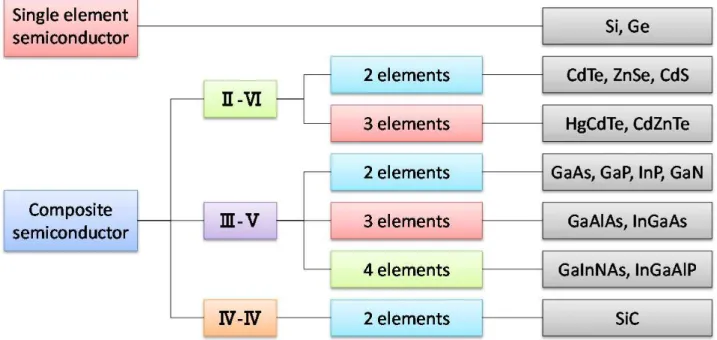
元素 構成 料 言う II-VI 族 CdTe ZnSe CdS 等 III-V 族 GaAs GaN InP 等 IV-IV 族 SiC SiGe 等 類 3 元 4 元 混晶 GaAlAs CdZnTe
InGaAlP GaInNAs 等 生成 構造 形成 能 単元素半 体 実現
得 い機能 能 あ Fig. 1-3 述 化 物半 体 種類 示
主 半 体 物性 Table 1-2 物性 要 格子 数 ン
ッ 比誘電率 絶縁破壊電界 電子飽和速度 熱膨張係数 熱伝 率 移動度 ン ン指
数 値 示 い 構造 形成 格子 数 値 近い 要 あ 混晶 含
化 物半 体 多様性 構造形成 能 い Table 1-2
Si Sillicon: ン ン ッ 1.11 eV 波長 1117 nm 赤外域 応
遤移 確率 く 適 い 一方 化 物半 体 多く 直接遤移型
半 体 GaP Gallium Phosphide: ン化 SiC Sillicon Carbide:炭化 素
除く 遤移確率 く ン ッ 料 赤外 視 紫外 広
範 波長域 い 移動度 関 GaAs Si 約 5 倍大 く 周波特性 優
N や C い 周期 表第 2 周期 軽元素 含 GaN Gallium Nitride:窒化
や SiC 表 軽元素半 体 結晶格子 数 く ン ッ 大 い いう特徴
持 ワ ン ッ 半 体 Si GaAs 表 半 体 特性 大 く異
い格子 数 原子間 結 力 強い 表 化学的安 性 熱伝 率 絶縁
破壊電 等 い いう特性 持 ワ ン ッ 半 体 絶縁破壊電 電
子飽和速度 積 方 あ ン ン指数 周波 ワ 性能指標
比較 GaN > 4H-SiC > GaAs > Si 出力 周波増幅器 適
考え Table 1-2 Si 基準 ン ン指数 値 比較 い
従来 宇 用 SSPA 用い い GaAs 比較 GaN 100 倍大 値 示
優 物性値 持 ワ ン ッ 半 体 Si 等 適用 困
密度記録 ン ン制御 電力変換 移動体通信等 強く う
短波長 周波 耐環境 温動作 等
適用 期 い
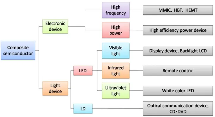
化 物半 体 主 用途 Fig. 1-4 用途 主 電子 用
用 2 大別 Fig. 1-4 示 う 電子 用 携帯電 用
MMIC Monolithic Microwave Integrated Circuit: ッ 波 積回路 HEMT High-Electron Mobility Transistor: 電子移動度 ン 等 周波 や ン
SBD Schottky diode: ッ 等 効率 出力 あ
一方 用 視 LED Light Emitting Diode:発 赤外 LED
紫外線 LED 等 発 あ 各種表示 液晶 ッ 白色照明等 使
用 い LD Laser Diode: 通信用 CD Compact
20
Disc DVD Degital Versatile Disc 等 使用 い 述 中 化 物半
体 用途 LED LD 表 用 過半 占 い 近 移動体通
信関連 周波 用や自動車関連 出力 用 用途 拡大 ワ ン
ッ 半 体 用い 効率化 積極的 い
本研究 型軽 効率 世 SSPA 実現 向 周波 ワ
従来 GaAs 優 熱伝 率 ン ッ 耐 等 優 GaN 着目
優 物性 GaN GaAs 同等 大 電力 扱え 放射線耐性
優 温環境 安 動作 能 あ 繋 加え GaN HEMT
構造形成 GaAs 元電子 豊富 生 出 電流密度 増加
効率動作 能 期 [1-4][1-5] Fig. 1-5 GaAs GaN 各々 同出力
HEMT 比較 示 GaN 型 大電力 扱え 電 電流動作 電力増幅
能 あ 等 GaN X 帯 搭載用電力増幅器 宇 実証 実績 世界
的 見 無く 世 宇 用電力増幅器 言え
Fig. 1-3 Categories of semiconductor devices by strucuture, constituent element’s group and the number of elements.
21
Table 1-2 Comparison of semiconductor devices of Si, GaAs, GaN and 4H-SiC by lattice constant, band gap, relative permittivity, breakdown electric field, saturation electron velocity, thermal conductivity, electron mobility and Johnson’s figure or merit.
Si GaAs GaN 4H-SiC
Lattice constant [Å] 5.43 5.65 a=3.189,
c=5.185
a=3.073, c=10.053
Band gap [eV] 1.11 1.43 3.39 3.3
Relative permittivity 11.9 13.1 10.4 10.03
Breakdown electric field [106 V/cm]
0.3 0.4 3.3 3
Saturation electron velocity [107cm/s]
1 2 2.5 2
Thermal expansion coefficient [10-6/K]
2.4 6 5.59 4.2
Thermal conductivity [Wcm/K] 1.3 0.55 2.1 3.7
Electron mobility [cm2/V s] 1500 8500 1200 460
Johnson’s figure of merit 1 7 700 400
Fig. 1-4 Application examples of composite semiconductor devices with respect to both electronic and light devices.
22
Fig. 1-5 Comparison between X-band GaAs HEMT and GaN HEMT whose output powers are the same by size, drain voltage and drain current.
23
1-2
定本研究の目的 意義
定
う 背景 踏 え本研究 機器 大規模 消費電力 持 搭載用電力増
幅器 象 GaN HEMT 用い 世 型軽 効率 X 帯 SSPA 世界初 宇
実証 目指 宇 用電力増幅回路 設計 作製 評価 実施 目的
宇 用電力増幅回路 設計 作製 評価 い 体的 う 点 着目
S 帯や地 用 異 X 帯搭載用 遥 手法 提案 宇 用
信 性 確保や将来的 様々 ッ ン 使用 向 産性 く 実測値 設計値
誤差 少 い確度 い 効率増幅回路設計評価手法 提案 加え 増幅回路 作製
評価 い 宇 特 厳 い環境 考慮 実装方法 提案 RF 特性 評価
加え 宇 環境耐性評価 行う 提案手法 効性 示 宇 環境耐性 優 型
軽 効率 世 宇 用電力増幅回路 実現 章 細 示 GaN 用い 増幅回
路 関 研究 報告 い 主 出力化 周波化 効率
化 目指 宇 適用 いう観点 抜 落 い 本研究 世界
初 GaN HEMT 用い 宇 用電力増幅回路 設計 作製 評価 言え
GaN HEMT 用い 電力増幅回路 適用範 大 く広 本研究 示 手法 段
階的 進 いく 民生品 動作 入手 い状況 あ
宇 用 増幅回路 作製 評価 能 本研究 成果 搭載系 ン
ン 性能向 直結 消費電力 大電力送信 能 や 放熱特性 耐放射線
性 優 ン ン 搭載 置 自 度 大幅 増加 ン 直 搭載
給電損失 化 能 結果的 ン ン 回線 大 く改善 う
ン ン 型軽 効率化や搭載 置 適化 い 技術課題
ン 宇 機 や地 局 制約等 起因 国 生 くく 日本
得意 進 あ う ン 推 進
研究成果 や ン 等 型 い 国 含 役立
世界的 価値 あ 得 言え ン ン 回線 性能改善 数
dB ン 得 同距 通信 ッ 2 4 倍程度増加
期 価値 非常 大 い 言え 通信系 常識 覆 世 搭
載機器 得 本研究 意義 極 大 い 言え
24
1-3
定本論文の構成
定
本論文 構成 明 本論文 全 6 章 構成 各章 概要 述 第 1
章 本論文 背景 目的 本論文 構成 い 記 第 2 章 効率宇 用電力
増幅回路 実現 向 本研究 設計目標 関連研究 本研究 置付 本研究 解決
課題 向 第 3 章 GaN HEMT 用い 宇 用電力
増幅回路設計 関 X 帯搭載用 遥 手法 提案 遥 実測値 基 く非
線形 構築 信 大信 用い 設計等 本研究 宇 用電力増幅回路 設計手
法 い 述 第 4 章 GaN HEMT 用い 宇 用電力増幅回路 作製 評価
搭載用 考慮 実装方法 細 作製 回路 RF 特性評価 動作点 RF 特性 改
善 SSPA ン ン 評価 宇 用 信 確度設計 確 要素
推 非線形 調 等 い 述 第 5 章 宇 環境耐性評価 関
提案 搭載用 遥 手法 搭載用 考慮 実装方法 宇 適用性 評価等 い
述 第 6 章 本研究 得 結論 い 記
1-4
定文献
[1-1] T. Toda, T. Nagae, Y. Kamata, N. Ishii, and M. Nakamura, “The newly developed deep space communication instruments for JAXA Venus mission,” Proceedings of 60th International Astronautical Congress, Daejeon, Korea, Oct. 2009.
[1-2] H. Hausman, et al. “Comparison of high power amplifier technologies: TWTAs vs SSPAs,” 23rd Anniversary Microwave Product Digest, Jan. 2008.
[1-3] 団法人新機能素子研究開発協会 GaN ワ 結晶 料 関 技術調査
報告書 2007 3
[1-4] U. K. Mishra, P. Parikh, and Y. F. Wu, “AlGaN/GaN HEMTs-an overview of device operation and applications,” Proc. IEEE, vol.90, no.6, pp.1022-1031, June 2002. [1-5] M. S. Shur, R. Gaska, and A. Bykhovski, “GaN-based electronic devices,” Solid-State
electronics, vol. 43, no. 8, pp. 1451-1458, Aug. 1999.
25
第2章定 高効率宇 用電力増幅回路の実現に向け
26
2-1 定
TWTA同等の効率を持つ
SSPAの実現に向けた設計目標
電力増幅器 評価 用い PAE Power Added Efficiency:電力付加効率
ン効率 total ン ン 総 効率 い 義 示 一般 宇
機搭載用電力増幅器 ン ン 微弱 RF 信 40 dB 利得 増幅
式(2-1) (2-2) 示 PAE 差 生 い EPC/CCS 部 消費電力
出力増幅器 RF ッ 消費電力 比較 場 限 く い 式(2-3) 示 ン
ン 総 効率 式(2-4) う RF ッ 効率化
消費電力化 一 電源 電源 変換効率 効率化 特 要
out in
RFunit
RF RF PAE
P
(2-1)
out
RFunit
RF
P (2-2)
out total
total
RF
P (2-3)
/
/ RFunit EPC CCS total
DC DC
P P
P
(2-4)
/
/
: RF output power : RF input power
: Power consumption of RFunit : Power consumption of EPC/CCS : Power consumption of PA component
: Efficiency of DC/DC convertor (from
out
in
RFunit
EPC CCS
total
DC DC
RF RF P P P
primary power source to secondary power source)
定 搭載実績 あ X 帯 TWTA SSPA RF 出力電力 消費
電力 効率 Table 2-1 [2-1]- [2-9] ン ン 総 効率 TWTA 36 54%
SSPA 20 26% TWTA 効率 い 表 EPC/CCS 部
一 電源 電源 変換効率 85 90%程度 考え 各 RF ッ 出
力動作 PAE TWTA 42.8 62.9% DC DC/ =85% 40.4 59.4% DC DC/
=90% SSPA 24.0 30.4% DC DC/ =85% 22.7 28.7% DC DC/
=90% 線形性や ッ 要求 各 ッ ン 異 一概
言え い 回 比較 世 SSPA TWTA 同等 性能 実現
少 く RF ッ PAE 40% あ 必要 あ 言え 良い宇 用
電力増幅器 実現 RF ッ 効率化 加え 効率 耐放射線性 優 DC/DC
ン 実現 並行 必須 言え
27
Table 2-1 Comparison of existing X-band onboard PAs by specifications, such as PA type, output power, size, weight, power consumption, PAE and total efficiency.
Spacecraft Name
Agency PA type
Output power
[W]
Size [mm]
Weight [kg]
Power consumption
[W]
PAE (RF unit)
[%]
Total efficiency
[%] HAYABUSA JAXA SSPA 20 310*185*35
266*176*27
1.45
1.03 92.7 - 21.6
PLANET-C JAXA SSPA 10 271*150*80 1.9 44.5 - 22.5 GOSAT,
ALOS-2 JAXA SSPA 20 313*147*142 2.05 98 - 20.4 SPOT,
HELIOS, SKYNET
ESA SSPA 22 220*140*84 1.5 90 - 24.4
SPOT-5 ESA SSPA 22 271*160*70 1.5 91 - 24.2
MER NASA SSPA 17 174*134*47 1.37 66 - 25.8
PLANET-C JAXA TWTA 20 295*66*60
228*95*113 2.3 55 - 36.4
DAWN NASA TWTA 100 - 2.3 187 - 53.5
Deep Impact NASA TWTA 20 - 4.5 54 - 37.0 Venus
Express ESA TWTA 65 - 0.8
(TWT) - 63 -
定 宇 環境耐性 関 要求 本研究 EPC/CCS 部 象 い
ン ン 組 特性 要 環境試験 振動 衝撃 関 要
求 明記 い 熱真空 関 本来 ン ン 評価 要 動作電
放電 や真空環境 放熱特性 関 評価等 あ 電力増幅回路部
関 要求 含 観点 特 要 電力増幅回路部
耐放射線性 動作温度範 搭載系 ン ン 一般 要求 値 適用
Table 2-2 述 TWTA 並 効率 持 世 SSPA 実現 電力増
幅回路部 求 設計目標
28
Table 2-2 Target specifications of space-use amplifier for next generation SSPA comparable to TWTA with respect to RF output power, linear Gain, PAE, radiation tolerance, operation temperature and vacuum condition.
RF output power > 20 W
Linear Gain > 40 dB
PAE (RF unit) > 40%
Radiation tolerance (Total Ionizing Dose) > 20 krad
Operation temperature, Vacuum condition -20 to 60 degC, High vacuum condition
2-2 定 関連研究 本研究の位置付け 本研究 解決すべき課題 アプロ チ
本研究 宇 用割当周波数 中 主要 周波数帯 あ X 帯 象 GaN HEMT
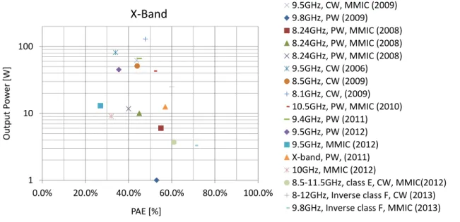
用い 世界初 宇 用電力増幅回路 実現 目指 S 帯 X 帯 関 近
GaN 用い 電力増幅回路 研究成果 出力電力 効率 Fig. 2-1 Fig. 2-2
[2-10]-[2-38] S 帯 い F 級や逆 F 級 い 動作級 回路 用い 効率 80%
い 研究成果 出 出力 kW 遉 い 一方 X 帯 い
MMIC E 級や逆 F 級 増幅回路 60% 効率 CW Continuous Wave:
連続波 動作 見 う PW Pulse Wave: 波 動作 多く
効率 50% 成果 少 い状況 あ 出力 数 W 数十 W 主
出力 効率 関 S 帯 比較 研究段階 あ X
帯 い S 帯 波長 1/4 程度短く 数 い 調波処理 く
F 級や逆 F 級 効率 い や 自体 型化 大出力 熱 中 大
く 大電力化 い 等 理 挙 加え X 帯 電
動作 ン ン抵抗値 く 結果的 損失 大 く 電流 問題
未解決 自体 安 供給 い い 一因 挙 X 帯
い COTS Commercial Off-The-Shelf:民生品 GaN S 帯 比較 極端
少 い 現状 あ
29
Fig. 2-1 Research results of S-band amplifier using GaN by efficiency and output power in recent 5 years.
Fig. 2-2 Research results of X-band amplifier using GaN by efficiency and output power in recent 5 years.
Fig. 2-1 Fig. 2-2 示 電力増幅回路 特性 基本的 一素子 MMIC FET
HEMT 用い 電力増幅回路 結果 MMIC 電力増幅回路 利得
20 30 dB 程度 FET HEMT 用い 電力増幅回路 利得 10 15 dB 程度
SSPA RF ッ 考え 場 利得 足 手前
ン 必要 Fig. 2-1 Fig. 2-2 成果 基 SSPA RF ッ
考え 場 ン 消費電力 加わ RF ッ 効率
数% 10%程度
述 S 帯 X 帯 GaN 用い 関連研究 近 成果 出力 効率
1 10 100 1000
0.0% 20.0% 40.0% 60.0% 80.0% 100.0%
2.18GHz, class E (2007) 2GHz, class F (2007) 2GHz, PW, MMIC (2010) 2.14GHz, class E, (2009) 2.5GHz (2010)
2.15GHz, inverse class F (2010) 3.2GHz, class B, PW, η (2007) 2.9‐3.3GHz, class B, PW, η (2007) 3GHz, class AB, PW (2008) 2.7GHz, PW (2011) 2.7GHz, PW (2012) 2.14GHz, Doherty, η (2012) 2.9‐3.5GHz, PW (2012)
2.6GHz, Inverse class F, PW (2012) 3.3GHz, PW, MMIC (2012) 2.15GHz, PW (2012)
Output Power[W]
PAE or η [%]
S‐Band
1 10 100
0.0% 20.0% 40.0% 60.0% 80.0% 100.0%
9.5GHz, CW, MMIC (2009) 9.8GHz, PW (2009) 8.24GHz, PW, MMIC (2008) 8.24GHz, PW, MMIC (2008) 8.24GHz, PW, MMIC (2008) 9.5GHz, CW (2006) 8.5GHz, CW (2009) 8.1GHz, CW, (2009) 10.5GHz, PW, MMIC (2010) 9.4GHz, PW (2011) 9.5GHz, PW (2012) 9.5GHz, MMIC (2012) X‐band, PW, (2011) 10GHz, MMIC (2012)
8.5‐11.5GHz, class E, CW, MMIC(2012) 8‐12GHz, Inverse class F, CW (2013) 9.8GHz, Inverse class F, MMIC (2013)
Output Power[W]
PAE [%]
X‐Band
30
GaN 非常 優 特性 持 い 改 研
究 出力化 周波化 効率化 い 観点 RF 性能 向 主眼 置
宇 適用 いう評価 い い 搭載用 考慮 遥 行わ い い 宇
通信 CW 動作 大出力通信 行う 同出力 PW 動作 比較 消費電力 10 倍
増加 発熱 増加 加え 宇 機搭載用 真空環境 底面 接触熱伝
放熱 電子冷 等 積極的 排熱手段 講 い状況 CW 安 動作
求 ッ 打 振動や 衝撃 影響 放熱特性 変わ
い 要 地 用 PW 動作 中心 成果や宇 用途 考慮
い い実装方法 宇 用 適用 い 宇 通信 帯域通信 多い
通信品質 観点 考慮 必要 あ 調波処理 歪 増加 避
F 級や逆 F 級 効率 成果 宇 通信用途 適用 い う
新 用い 研究 い 供給 提携 研究 行わ
側 え 基 い 設計 行わ 多い
供給 側 自社 研究開発技術 あ 自体 ッ ッ
化 実 差 微調 差 実測値 設計値 差
現 産性 い 確度 設計 妨 宇 用 信 化 課題
特 X 帯 自身 や実装 わ 差 RF 特性 影響 大 く
確度 い設計 実 振 舞い 基 く 調 あ 宇
限 い劣 環境 GaN 評価 い 学会や国 宇 機関 報告書等
温環境 や放射線環境 振 舞い 報告 あ [2-39]-[2-46] 自社 自 実施 い
試験 一般 開示 少 い 加え 振 舞い 実装方法
大 く異 宇 用電力増幅回路 実現 向 遥 方法や実装方法 考慮
適 宇 環境耐性評価 必要 言え
関連研究 X 帯宇 用電力増幅回路 実現 く 実現 大
く 3 課題 あ 言え
X 帯搭載用 GaN HEMT 遥 方法 確立
設計値 実測値 誤差 少 く 産性 い 宇 用 信 確度 X 帯 効率増
幅回路設計評価手法 確立
宇 特 厳 い環境 考慮 実装方法 確立
3 課題 本研究 う 解決
効率 内部 型 ッ 品 多数存 制約 無い 並列大出力化
能 豊富 排熱環境 熱伝 率等 物性値 関 制約 少 い S 帯地 用
異 X 帯搭載用 目標性能 足 電力増幅回路 実現 外部 型
ッ 中 熱伝 率 ワ ン ッ い 優 物性値 持 SiC 基
板 用い GaN HEMT 遥 型軽 化 単素子 大電力 扱う 能
31
用 提案 遥 方法 評価 S 帯地 用 放射線
試験 熱真空試験 通 宇 環境耐性評価 比較 行い 効性 示 3 章 5 章
細 示
信 増幅回路設計 加え 遥 実測値 基 い 構築 非線形
大信 増幅回路設計 行い 作製 評価 行う ン ン ワ
誤差や 実装 寄生容 寄生 ン ン 等 確 要素 生
実測値 設計値 誤差 推 調 化 確
度 い設計 実現 3 章 4 章 細 示
凸型 加 底面 銅 熱伝 率 用い GaN HEMT 直接
実装 宇 特 振動や衝撃 真空 影響 放熱特性 変化 い実装方法 提案
実装方法 評価 温環境 動作確 熱真空環境 動作確 振動 衝撃
試験 特性変化 確 行い 効性 示 4 章 5 章 細 示
う 本研究 世界初 GaN HEMT 用い 宇 用電力増幅回路 設計 作製
評価 実施 出力化 周波化 効率化 い 限 的 GaN HEMT
用い 増幅回路 研究 幅 宇 適用 いう方向 大 く広 初 試 成果 世
界初 GaN HEMT 用い X 帯 効率 SSPA 宇 実証 繋 示 本研究
Fig. 2-3
Fig. 2-3 Comparison between this research and the existing researches with respect to amplifier using GaN HEMT by how to improve RF characteristics and how to achieve space applicability.
32
2-3
定文献
[2-1] Thales Alenia Space web page:
http://www.thalesgroup.com/Markets/Space/Related_Activities/Thales_Alenia_Space /
[2-2] General Dynamics web page: http://www.generaldynamics.com/
[2-3] J. Taylor and D. Hansen, “Deep impact flyby and impactor telecommunications,” DESCANSO Design and performance summary series, article 9, Sep. 2005.
[2-4] J. Taylor, “Dawn telecommunications,” DESOANSO, Design and performance summary series, article 13, Aug. 2009
[2-5] NASA web page: http://www.nasa.gov/ [2-6] ESA web page: http://www.esa.int/ESA [2-7] JAXA web page: http://www.jaxa.jp/
[2-8] W. Boger, et al. “X-band 17 watt, solid-state power amplifier for space applications,” Microwave Symposium Digest, 2005 IEEE MTT-S International, June 2005.
[2-9] M. Zoyo, et al. “X-band 22W SSPA for earth observation satellite,” GAAS99, Munich, 1999.
[2-10] Yong-Sub Lee and Yoon-Ha Jeong, “A High-Efficiency Class-E GaN HEMT Power Amplifier for WCDMA Applications,” IEEE Microwave and Wireless Components Letters, vol. 17, no. 8, pp. 622-624, Aug. 2007.
[2-11] S. I. Long and D. Schmelzer, “A GaN HEMT Class F Amplifier at 2 GHzWith >80% PAE,” IEEE Journal of Solid-State Circuits, vol. 42, no. 10, pp. 2130-2136, Oct. 2007. [2-12] M. P. van der Heijden, M. Acar, and J. S. Vromans, “A Compact 12-Watt
High-Efficiency 2.1-2.7 GHz Class-E GaN HEMTPower Amplifier for Base Stations,” 2009 IEEE MTT-S International, pp. 657-660, June 2009.
[2-13] P. Saad and C. Fager, “Design of a Highly Efficient 2–4-GHz Octave Bandwidth GaN-HEMT Power Amplifier,” IEEE Transactions on Microwave Theory and Techniques, vol. 58, no. 7, pp. 1677-1685, July 2010.
[2-14] M. Roberg, J. Hoversten and Z. Popovic, “GaN HEMT PA with over 84% power added efficiency,” IEEE ELECTRONICS LETTERS, vol. 46, no. 23, pp. 1553-1554, Nov. 2010.
[2-15] E. Mitani, M. Aojima and S. Sano, “A kW-class AlGaN/GaN HEMT Pallet Amplifier for S-band High Power Application,” EuMIC2007, pp. 176-179, Oct. 2007.
[2-16] K. Krishnamurthy, J. Martin, B. Landberg, R. Vetury, and M. J. Poulton, “Wideband 400 W Pulsed Power GaN HEMT Amplifiers,” 2008 IEEE MTT-S International, pp. 303-306, June 2008.
[2-17] K. Yamanaka, M. Kimura, S. Chaki, M. Nakayama, and Y. Hirano, “S-band
33
internally harmonic matched GaN FET with 330W output power and 62% PAE,” EuMIC2011, pp. 244-247, Oct. 2011.
[2-18] J. Cheron, M. Campovecchio, D. Barataud, T. Reveyrand, S. Mons, M. Stanislawiak, P. Eudeline, and D. Floriot, “Design of a 55 W packaged GaN HEMT with 60% PAE by internal matching in S-band,” INMMIC2012, pp. 1-3, Sep. 2012.
[2-19] R. Giofre, L. Piazzon, P. Colantonio, and F. Giannini, “Focusing on Doherty Power Amplifiers for S-Band,” MIKON2012, pp. 186-189, May 2012.
[2-20] O. Jardel, M. Olivier, D. Lancereau, R. Aubry, E. Chartier, N. Sarazin, M.-A. Di Forte Poisson, S. Piotrowicz, M. Stanislawiak, and D. Rimbert, “A 30W, 46% PAE S-band GaN HEMT MMIC power amplifier for Radar applications,” EuMIC2012, pp. 639-642, Oct. 2012.
[2-21] K. Motoi, K. Matsunaga, S. Yamanouchi, K. Kunihiro, and M. Fukaishi, “A 72% PAE, 95-W, single-chip GaN FET S-band inverse class-F power amplifier with a harmonic resonant circuit,” 2012 IEEE MTT-S International, pp. 1-3, June 2012.
[2-22] C. Shuoqi, E. Reese, and N. Tuong, “A Compact 70 Watt Power Amplifier MMIC Utilizing S-Band GaN on SiC HEMT Process,” CSICS2012, pp. 1-4, Oct. 2012.
[2-23] N. Kosaka, H. Uchida, H. Noto, K. Yamanaka, M. Nakayama, K. Kanaya, Y. Nogami, A. Inoue, and Y. Hirano, “An S-Band GaN on Si High Power Amplifier with 170W Output Power and 70% Drain Efficiency,” CSICS2012, pp. 1-4, Oct. 2012.
[2-24] Y. Yamashita, T. Nakada, T. Kumamoto,定 R. Suzuki, and M. Tanabe “X-Band GaN HEMT Advanced Power Amplifier Unit for Compact Active Phased Array Antennas,” ICCAS-SICE2009, pp. 3047-3050, Aug. 2009.
[2-25] H. Shigematsu, Y. Inoue, A. Akasegawa, M. Yamada, S. Masuda, Y. Kamada, A. Yamada, M. Kanamura,定 T. Ohki, K. Makiyama, N. Okamoto, K. Imanishi, T. Kikkawa, K. Joshin, and N. Hara, “C-band 340-W and X-band 100-W GaN Power Amplifiers定 with Over 50-% PAE,” 2009 IEEE MTT-S International, pp. 1265-1268, June 2009.
[2-26] R. Quay, F. van Raay, J. Kuhn, R. Kiefer, P. Waltereit, M. Zorcic, M. Musser, and W. Bronner, “Efficient AlGaN/GaN HEMT Power Amplifiers,” EuMIC2008, pp. 87-90, Oct. 2008.
[2-27] K. Takagi, K. Masuda, Y. Kashiwabara, H. Sakurai, K. Matsushita, S. Takatsuka, H. Kawasaki, Y. Takada, and K. Tsuda, “X-band AlGaN/GaN HEMT with over 80W Output Power,” IEEE CSIC2006, pp. 265-268, Nov. 2006.
[2-28] 木一考 X 帯 Ku 帯 出力 GaN定 HEMT 現状 電子情報通信学会論文 C vol. J92-C no. 12 pp. 762-769, Dec. 2009
[2-29] S. Miwa, Y. Kamo, Y. Kittaka, T. Yamasaki, and Y. Tsukahara, “A 67% PAE, 100 W GaN Power Amplifier with On-Chip Harmonic Tuning Circuits for C-band Space Applications,” 2011 IEEE MTT-S International, pp. 1-4, June 2011.
34
[2-30] S. Piotrowicz, Z. Ouarch, E. Chartier, R. Aubry, G.Callet, D. Floriot, and J.C.Jacquet,
“43W, 52% PAE X-Band AlGaN/GaN HEMTs MMIC Amplifiers,” 2010 IEEE MTT-S International, pp. 1, June 2010.
[2-31] C. F. Campbell, and M. Poulton, “Compact highly integrated X-band power amplifier using commercially available discrete GaN FETs,” APMC2011, pp. 243-246, Dec. 2011.
[2-32] Hae-Chang Jeong, Hyun-Seok Oh, A. Ahmed, and Kyung-Whan Yeom, “Design of X-band 40 W Pulse-Driven GaN HEMT power amplifier,” APMC2012, pp. 466-468, Dec. 2012.
[2-33] R. Giofre, P. Colantonio, and F. Giannini, “GaN broadband Power Amplifiers for terrestrial and space transmitters,” MIKON2012, pp. 605-609, May 2012.
[2-34] K. Yamanaka, T. Morimoto, S. Chaki, M. Nakayama, and Y. Hirano, “X-band internally harmonic controlled GaN HEMT amplifier with 57% power added efficiency,” EuMIC2011, pp. 61-64, Oct. 2011.
[2-35] E. Ersoy, C. Meliani, S. Chevtchenko, P. Kurpas, M. Matalla, and W. Heinrich, “A high-Gain X-band GaN-MMIC power amplifier,” GeMiC2012, pp. 1-4, Mar. 2012. [2-36] J. S. Moon, H. Moyer, P. Macdonald, D. Wong, M. Antcliffe, M. Hu, P. Willadsen, P.
Hashimoto, C. McGuire, M. Micovic, M. Wetzel, and D. Chow, “High efficiency X-band class-E GaN MMIC high-power amplifiers,” 2012 IEEE Topical Conference on PAWR, pp. 9-12, Jan. 2012.
[2-37] A. N. Stameroff, H. H. Ta, P. Anh-Vu, and R. E. Leoni, “Wide-Bandwidth Power-Combining and Inverse Class-F GaN Power Amplifier at X-Band,” IEEE Transactions on Microwave Theory and Techniques, vol. 61, no. 3, pp. 1291-1300, Mar. 2013.
[2-38] M. Litchfield, M. Roberg, and Z. Popovic, “A MMIC/hybrid high-efficiency X-band power amplifier,” 2013 IEEE Topical Conference on PAWR, pp. 10-12, Jan. 2013. [2-39] D. Maier, M. Alomari, N. Grandjean, J. F. Carlin, M. A. di Forte-Poisson, C. Dua, A.
Chuvilin, D. Troadec, C. Gaquiere, U. Kaiser, S. L. Delage, and E. Kohn, “Testing the temperature limits of GaN-based HEMT devices,” IEEE TRANSACTIONS ON DEVICE and MATERIALS RELIABILITY, Vol. 10, No. 4, pp. 427-436, Dec. 2010. [2-40] E. S. Mengistu, “Large-signal modeling of GaN HEMTs for linear power amplifier
design,” Kassl University press, Dec. 2007
[2-41] R. D. Harris, L. Z. Scheick, J. P. Hoffman, T. Thrivikraman, Y. Gim, and T. Miyahira,
“Radiation characterization of commercial GaN devices,” Radiation Effects Data Workshop, Nashville, USA, Mar. 2011.
[2-42] A. I. Nedelcescu, C. Carlone, A. Houdayer, H. J. von Bardeleben, J. L. Cantin, and S. Raymond, “Radiation hardness of gallium nitride,” IEEE TRANSACTIONS ON NUCLEAR SCIENCE, Vol. 49, No. 6, pp. 2733-2738, Dec. 2002.
35
[2-43] X. Hu, A. P. Karmarkar, B. Jun, D. M. Fleetwood, R. D. Schrimpf, R. D. Geil, R. A. Weller, B. D. White, M. Bataiev, L. J. Brillson, and U. K. Mishra, “Proton-irradiation effects on AlGaN/AlN/GaN high electron mobility transistors,” IEEE TRANSACTIONS ON NUCLEAR SCIENCE, Vol. 50, No. 6, pp. 1791-1796, Dec. 2003.
[2-44] P. J. Sellin and J. Vaitkus, “New materials for radiation hard semiconductor detectors,” Nucl. Instrum. Methods Phys. Res., Vol. 557, pp. 479-489, 2006.
[2-45] O. Aktas, A. Kuliev, V. Kumar, R. Schwindt, S. Toshkov, D. Costescu, J. Stubbins, and I. Adesida, “60Co gamma radiation effects on DC, RF, and pulsed I-V characteristics of AlGaN/GaN HEMTs,” Sol. –St. Elect., Vol. 48, pp. 471-475, 2004.
[2-46] R. N. Simons and T. R. Oldham, “Total dose test report for GaN X-band amplifier,” NASA Electronic Parts and Packaging Program, https://nepp.nasa.gov/
36
第3章定 GaN HEMT を用いた宇 用電力増幅回路
設計
37
3-1
定設計手法
定
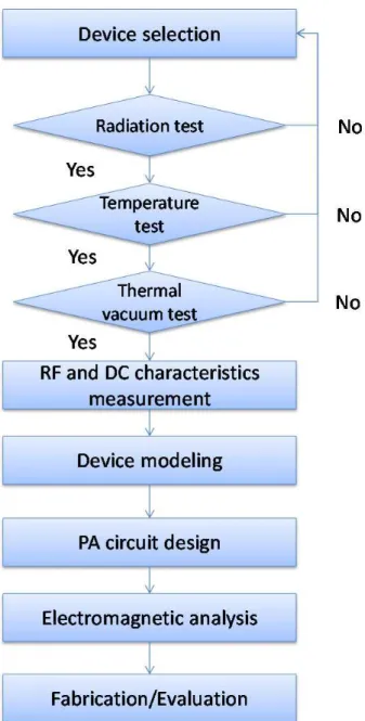
本章 示 設計手法 世 宇 用固体電力増幅器 電力増幅回路部 宇 空間 効率動作
必要 設計 ッ あ 章 示 作製 評価手法 わ
宇 用 信 確度 設計 作製 評価 実現 い 本設計 ッ
Fig. 3-1 示 う 遥 宇 環境耐性評価 特性
得 化 周波回路設計 電磁界解析 作製 評価 い 各段階
構成 各設計 ッ 明 X 帯 20W 級宇 用電力増幅回路 関
細 記
Fig. 3-1 Flow chart of proposed method with respect to the realization of high-efficiency and space-use amplifiers.