Design of the Energy Structures of
Photovoltaic Organic Co-deposited Films
by Impurity Doping
2013
Norihiro Ishiyama
Preface
This thesis was performed under the guidance of Professor Masahiro Hiramoto at Department of Functional Molecular Science, School of Physical Sciences, The Graduate University for Advanced Studies.
The aim of this work is to develop doping technique in order to design the appropriate energy structures of photovoltaic co-deposited films for high efficient organic solar cells.
The author believes that techniques developed in this thesis will lead to the development of a high-efficient organic solar cell.
Norihiro Ishiyama
Department of Functional Molecular Science School of Physical Sciences
The Graduate University for Advanced Studies
March 2013
Contents
Chapter 1: General Introduction 1
1.1. Background 1
1.2. Overview of this Thesis 2
1.3. History of Organic Photovoltaic Cells 3
1.4. Donor/Acceptor Sensitization 8
1.5. Impurity Doping 11
1.6. Aim of this Thesis 15
1.7. References 17
Chapter 2: Fundamental Equipment and Methods 21
2.1. Purification of Materials 21
2.2. Fabrication of Cells 23
2.3. ‘Three Component Co-evaporation’ Technique 26
2.4. Measurements of Photovoltaic Properties 28
2.5. Kelvin Probe Measurements 32
2.6. Energy Band Mapping of Doped Junctions 34
2.7. References 36
Chapter 3: Function Control of pn-Homojunctions and the Formation of Tandem Photovoltaic Cells in Single Fullerene Films
37
3.1. Introduction 38
3.2. Experimental 39
3.3. Results and Discussion 41
3.3.1. Exploration of a Donor Dopant 41
3.3.2. Control of Fermi Levels in Single C60 Films by Doping with MoO3 and Cs2CO3
44
3.3.3. n+p+-C60 Homojunction Acting as an Ohmic Interlayer 46 3.3.4. Energy Band Diagram of a Tandem C60 Photovoltaic Cell 48
3.4. Conclusion 52
3.5. References 53
Chapter 4: Control of the Conduction Types of Photovoltaic Co-deposited Films by Doping with Molybdenum Oxide
56
4.1. Introduction 57
4.2. Experimental 58
4.3. Results and Discussion 61
4.3.1. Positive Shift of Fermi Level in a Co-deposited Film Consisting of C60 and α-Sexithiophene (C60:6T) by MoO3 Doping
61
4.3.2. Tuning of Conduction Type in C60:6T Films by MoO3 Doping 63 4.3.3. Potential Profiles of MoO3-doped C60:6T Cells 68
4.4. Conclusion 68
4.5. References 69
Chapter 5: Control of the Barrier Parameters of n-Type Schottky Junctions in Photovoltaic Co-deposited Films by Doping with Cesium Carbonate
71
5.1. Introduction 72
5.2. Experimental 73
5.3. Results and Discussion 74
5.3.1. Formation of Cs2CO3-doped n-Type C60:6T Schottky Junctions 74 5.3.2. Barrier Parameters and Doping Efficiency in Cs2CO3-doped C60:6T
Cells
76
5.4. Conclusion 83
5.5. References 84
Chapter 6: Doping-based Design of Organic Solar Cells in Co-deposited Films 86
6.1. Introduction 87
6.2. Experimental 88
6.3. Results and Discussion 90
6.3.1. Design of p+in+-C60:6T Homojunction Cells 90
6.3.2. Design of a Tandem C60:6T Solar Cell 91
6.3.3. Energy Band Diagram of a Tandem C60:6T Solar Cell 94
6.4. Conclusion 98
6.5. References 99
Chapter 7: General Conclusion 101
7.1. Summary of this Thesis 101
7.2. Future Prospects 107
List of Publications 108
List of Supplementary Publications 109
Poster Presentations in International Conferences 110
Oral Presentations in Conferences 110
List of Books 111
Acknowledgement 112
1
Chapter 1:
General Introduction
1.1. Background
Currently, problems related to energy generation have been increasing all over the world. Since electrical power has traditionally been generated using fossil fuels such as oil, coal, and natural gas over the long term, these non-renewable resources are drying up. In addition, nuclear fuel, which has been used as an alternative energy resource, carries with it the serious risk of environmental pollution. Therefore, renewable and clean energy sources must be developed as rapidly as possible.
Photovoltaic energy conversion, which can generate direct-current electricity from solar radiation by utilizing solar cells, is a possible candidate to replace the conventional power generation systems. Photovoltaic systems are superior to the conventional systems in many ways, such as the free energy source supplied from the sun, freedom of location, and environmental harmony. However, conventional solar cells consisting of crystalline silicon or gallium compounds are too expensive to become universally applied. Hence, low-cost solar cells must be developed.
Organic solar cells, which consist of thin films of organic semiconductor material produced by printing or vacuum deposition at low temperature, are one example of such a low-cost cell. They have many advantages over conventional inorganic cells, including their light-weight properties and ease of manufacture by
‘roll-to-roll’ printing onto flexible plastic sheets. Therefore, organic solar cells have the potential to be applied to many different fields, such as mobile devices, ‘wrap’
2
advertising applications, and building components. However, the photoelectric conversion efficiency of organic solar cells is still lower than that of conventional cells.1) For commercial use, the efficiency must be improved by making a breakthrough in the design of the structures of these cells.
1.2. Overview of this Thesis
This thesis focused on organic solar cells consisting of vacuum-deposited films. Most recent cells include co-deposited films, which consist of two kinds of organic semiconductors, in order to generate significant photocurrent densities. On the other hand, doping-based control of the energy structures of organic solar cells is a significant challenge, as it is in the case of inorganic cells. In particular, there has been no attempt to control the pn-properties of organic co-deposited films by doping.
In this thesis, the author developed doping techniques in order to design the energy structures of photovoltaic organic co-deposited films.
A co-deposited film consisting of fullerene and α-sexithiophene (C60:6T), which shows a large open circuit voltage reaching 0.8 V, was used.2,3) Molybdenum oxide (MoO3)4,5,6) and (Cs2CO3)7,8) were used as the acceptor and donor dopants, respectively. In order to dope into the co-deposited films, the author developed a
‘three component co-evaporation’ technique, in which three different evaporation sources were used. Precise monitoring of the deposition rates of the dopants using a computer monitoring system enabled us to dope as low as 40 ppm by volume concentration. In order to clarify the operation mechanisms of doped junctions,
3
‘energy-band mapping’ using Kelvin probe and capacitance measurements was employed.
The pn-properties of C60:6T co-deposited films could be completely controlled by doping with MoO3 and Cs2CO3. A series of fundamental doped junctions, that is, p-type and n-type Schottky junctions, pn, p+in+, and ohmic n+p+ homojunctions, and ohmic junctions between metal electrodes and heavily doped p+ and n+ layers were fabricated. Based on these doping techniques, a tandem organic solar cell was formed in a C60:6T co-deposited film by connecting two photoactive p+in+-homojunctions with an n+p+-ohmic interlayer. The open circuit voltage and the conversion efficiency of the tandem cell reached 1.69 V and 2.4%, respectively.
1.3. History of Organic Photovoltaic Cells
Although research into organic photovoltaic cells started in 1958,9) early cells, which consisted of single molecular layers, generated very little photocurrent.10,11) In 1986, Tang developed a pn-heterojunction cell consisting of copper phthalocyanine (CuPc) and perylene-derivative (Im-PTC) films (Fig. 1.1(a)).12) For this cell, the short-circuit photocurrent density (Jsc) and the conversion efficiency were 2.3 mA cm-2 and 1% respectively under simulated solar light, which were much larger than the values reported previously. Since donor/acceptor (D/A) sensitization (see also section 1.4) was induced, the efficiency of free-carrier generation was considerably increased.
However, a significant problem still remained in terms of the cell structure. Since the diffusion length of excitons in organic semiconductors is as short as several nanometers, only excitons generated in a narrow area (around 10 nm) adjacent to the D/A interface
4
can reach the site where dissociation occurs.13) Namely, excitons generated in regions distant from the D/A interface cannot be dissociated. Thus, regions that are remote from the D/A interface become ‘dead layers’ that do not generate photocurrent. Ten nanometer-thick layers were too narrow to absorb sufficient photons to generate significant photocurrent densities.
Fig. 1.1 Structures of Donor/Acceptor heterojunction cells and carrier transport mechanisms.
(b) pin-Heterojunction cell Acceptor
Electrode
Electrode Donor
hν Donor: Acceptor
(Active region)
p-layer n-layer
i-layer p-layer
n-layer
(a) pn-Heterojunction cell Electrode
Electrode Acceptor
Donor
hν Active region
5
In 1991, Hiramoto et al. proposed a pin-heterojunction cell that incorporated a co-deposited film consisting of metal-free phthalocyanine and a perylene derivative (H2Pc:Me-PTC) (Fig. 1.1(b)).14,15) In the case of the pin cell, the value of Jsc was almost doubled compared to that of the pn-heterojunction cell. Since the molecules of H2Pc and Me-PTC are mixed on the nanoscale, there are in effect D/A interfaces throughout the whole of the H2Pc:Me-PTC co-deposited films. That is, photocurrent could be generated within the whole of the co-deposited film, which therefore absorbs a significant portion of the incident light. Thus, the active region for photocurrent generation could be extended by forming a pin-heterojunction cell.
Since then, many researchers have attempted to improve the photovoltaic performance of pin-heterojunction cells. Peumans et al. demonstrated control of the morphology of a D/A co-deposited film by annealing. 16) On the other hand, Taima et al. reported on the need for optimizing the film thickness of each layer. 17) In addition, there have been many efforts to improve the fabrication processes in order to enhance the efficiency of pin-heterojunction cells.18-22)
Organic photovoltaic materials have also been actively researched (Fig. 1.2). Early cells used perylene derivatives as acceptor materials.12-16) In 1993, N. S. Sariciftci et al. reported that fullerene (C60) acted as an excellent acceptor material.23) Currently, C602,17-22,24-30)
and C703,31) have become the fundamental acceptor materials of choice. Many different materials have been developed as donor materials to enhance the conversion efficiency. In order to generate significantly high Jsc values of more than 10 mA cm-2, materials such as phthalocyanines that possess high absorption-coefficients have been used.19-21) In addition, materials that exhibit near-infrared absorption have been used to extend the absorption wavelength
6
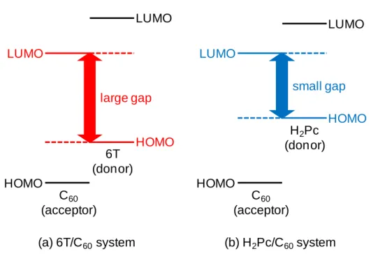
region.24-26) On the other hand, open-circuit voltage (Voc) is also a key factor that affects the efficiency of solar cells. The absolute value of Voc is limited by the energy difference between the HOMO level of the donor and the LUMO level of the acceptor (HOMO-LUMO gap) (Fig. 1.3). Since the upper edge of the gap is determined by the LUMO of C60, deep-lying HOMO-level donor materials have been investigated. For example, a combination of α-sexithiophene and C60, which has a large HOMO-LUMO gap (Fig. 1.3(a)), exhibits a large Voc value of more than 0.7 V, 2) while a combination of H2Pc and C60, which has a small gap (Fig. 1.3(b)), exhibits a Voc value of 0.4 V. So, in order to improve Voc values, conjugated oligothiophenes,22,27,28) merocyanine dyes,29) and rubrene30) have been used as donor materials.
Fig. 1.2 Organic photovoltaic materials. fullerene (C60) fullerene (C70)
phthalocyanine (H2Pc) α-sexithiophene (6T)
NH N
N N N H N
N N
S S
S S
S S
7
Fig. 1.3 Mechanism for the generation of open-circuit voltage.
Fig. 1.4 Structure of a tandem organic photovoltaic cell incorporating Au nanoparticles as an ohmic interlayer.
6T (donor) C60
(acceptor) LUMO
HOMO
LUMO
large gap
HOMO
(a) 6T/C60system
H2Pc (donor)
LUMO
HOMO small gap
C60
(acceptor) LUMO
HOMO
(b) H2Pc/C60system
Electrode
Acceptor Donor
hν Acceptor
Donor
Electrode
Au nanoclusters (Ohmic interlayer) Front cell
Back cell
8
Tandem cell formation is an effective method for doubling the Voc value. In 1990, Hiramoto et al. proposed a tandem cell incorporating Au nanoparticles connecting two pn-heterojunction cells (Fig. 1.4).32) Since then, other materials such as metal clusters,33-37) metal oxides,38-40) and organic materials41) have been used for the ohmic interlayers. Currently, Timmreck et al. have reported on ohmic interlayers consisting of doped transparent organic semiconductors.42-44)
1.4. Donor/Acceptor Sensitization
External quantum efficiency (EQE) is one important parameter for evaluating the performance of solar cells. EQE is expressed as the ratio of the number of electrons produced by photo irradiation to the number of photons irradiated to the cell. The EQE of an organic solar cell can be represented by Eq. (1.1).
EQE =�α×�ed×�ct×�cc (1.1)
ηα: the efficiency of absorption (causing the formation of an exciton, which is a bound state consisting of a hole and an electron).
ηed: the efficiency of exciton diffusion to sites for dissociation.
ηct: the probability of dissociation of excitons to free holes and electrons via charge transfer processes.
ηcc: the efficiency of carrier transport to the contacts, resulting in carrier collection by the corresponding electrode.
The magnitude of the exciton binding energy (F) obeys Coulomb’s Law (Eq. (1.2)).
� =
4���10
�1�2
�2 (1.2)
9
This equation consists of a specific dielectric constant (ε), the dielectric constant of a vacuum (ε0), the magnitudes of the charges (q1 and q2), and the distance between the charges (r). In the case of materials with large ε values, the exciton binding energy is small. In the case of inorganic solar cells, since the ε values of Si and GaAs are as high as 12 and 13, respectively, excitons formed under photo irradiation have significantly larger radii; much larger than 10 nm. Thus, the excitons can be easily dissociated to free holes and electrons by the application of heat at room temperature, and a photocurrent is generated immediately.
On the other hand, organic solar cells have a problem in terms of exciton dissociation. Since the ε values of organic semiconductors are as low as 4,45,46) the radii of any photo-induced excitons are around 1 nm. The exciton, in which a hole and an electron interact strongly with each other, is localized at an independent molecule (Frenkel exciton) (Fig. 1.5(a)). Thus, for single molecular films, the excitons are rarely dissociated and are almost immediately deactivated. As a result, ηct is extremely low and photocurrents as low as 0.1 mA cm-2 are generated in cells consisting of single molecular films.5,6,10,11)
On the other hand, for a combination of donors (D) and acceptors (A) consisting of two kinds of organic semiconductors that have different HOMO-LUMO levels from each other, the deactivation of excitons is avoided due to the formation of
‘charge-transfer’ (CT) excitons (Fig. 1.5(b)). Namely, the excitation of the acceptor is immediately followed by charge-transfer between the HOMO of the donor and the HOMO of the acceptor. The CT exciton can be easily dissociated into a free hole and an electron. Thus, ηct becomes considerably higher than the equivalent values in
10
single molecular films. As a result, photocurrents of significant magnitude are generated in cells that make use of D/A sensitization.
Fig. 1.5 Mechanisms of carrier generation in organic photovoltaic cells. 1. excitation 2. deactivation
(a) single molecular system LUMO
HOMO
+ _
Frenkel exciton molecule
donor
acceptor LUMO (A)
HOMO (A)
(b) Donor/acceptor system
1. excitation 2. charge transfer LUMO (D)
HOMO (D)
+ _
Charge transfer exciton donor
acceptor
11
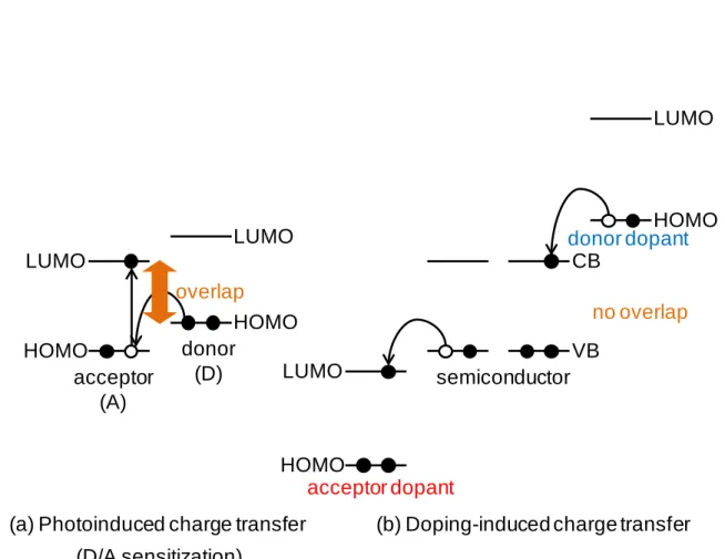
1.5. Impurity Doping
Doping-based control of the energy structure is a matter of great importance for organic solar cells.47) Impurity doping, which enables control of the conduction type and the reduction of the bulk resistance in a semiconductor, induces charge-transfer between a semiconductor and a dopant. When there is an overlap in energy regions between the band-gaps of two organic semiconductors, photoinduced CT (D/A sensitization) occurs (Fig. 1.6(a)) (see also section 1.4). On the other hand, in cases where there is no overlap in the band-gaps, doping-induced CT can be caused (Fig. 1.6(b)). For p-type doping, an acceptor dopant withdraws an electron from the valence
band (VB) of a semiconductor, that is, the dopant injects a hole into the VB of the semiconductor. For n-type doping, a donor dopant injects an electron into conduction band (CB) of the semiconductor. Thus, the characteristics of organic semiconductors can be controlled by impurity doping.
In the case of organic solar cells, doping has mainly been applied for making ohmic contacts at hetero interfaces.48,49) Leo et al. proposed the use of organic dopants for the formation of ohmic metal/organic contacts.50,51) 2,3,5,6-Tetrafluoro-7,7,8,8- tetracyanoquinodimethan (F4-TCNQ) and acridine orange base (AOB) were used as acceptor and donor dopants, respectively (Fig. 1.7). Currently, heavily-doped organic pn-heterojunctions have been used for the ohmic interlayers of tandem organic photovoltaic cells.42-44)
12
Fig. 1.6 Difference in charge-transfer mechanisms between D/A sensitization and doping.
Fig. 1.7 Dopants for organic semiconductors. donor
acceptor (D) (A) LUMO
HOMO
LUMO
HOMO
(a) Photoinduced charge transfer (D/A sensitization)
overlap
CB
VB semiconductor
acceptor dopant
donor dopant
LUMO
HOMO
(b) Doping-induced charge transfer HOMO
LUMO
no overlap
F4-TCNQ (p-type dopant)
AOB (n-type dopant)
13
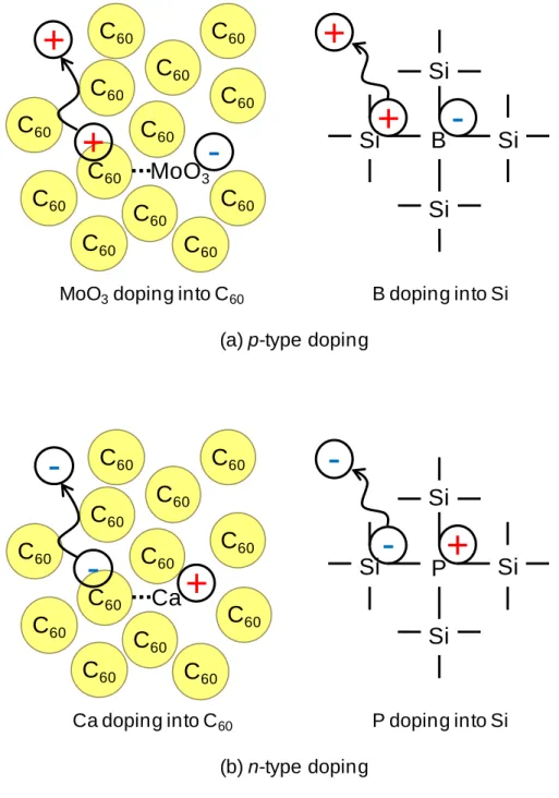
Fig. 1.8 Mechanism of doping into single C60 films.
On the other hand, the design of the energy structures such as pn, pin, and p+n+-homojunctions, in organic semiconductors is also a key issue, just as it is in Si and GaAs devices.47,52) In early works, the formation of pn-homojunctions in perylene
C
60MoO
3C
60C
60C
60C
60+ -
C
60C
60C
60C
60C
60C
60C
60C
60+
MoO3doping into C60
B
Si Si
Si
Si
+ -
+
B doping into Si (a) p-type doping
C
60Ca
C
60C
60C
60C
60+
-
C
60C
60C
60C
60C
60C
60C
60C
60-
Ca doping into C60
Si P Si
Si
Si
- +
-
P doping into Si (b) n-type doping
14
derivatives53) and in zinc phthalocyanine54) was demonstrated. Recently, Kubo et al. reported pn-control and pn-homojunction formation in single C60 films by doping with molybdenum oxide (MoO3) and Ca.5,6) For MoO3-doped C60, since the work function of MoO3 (6.7 eV) is more positive than the VB of C60 (6.4 eV), MoO3 accepts electrons from C60 (Fig. 1.8(a)) and forms charge-transfer complexes, i.e., C60+--- MoO3-. Here, the negative charge can be regarded as a spatially-fixed ionized MoO3 acceptor. The positive charge on C60+ can be liberated by thermal energy at room temperature and acts as a free hole in the VB of C60, making it p-type. This process is similar to P doping into Si. On the other hand, in the case of Ca-doped C60, since the work function of Ca (1.9 eV) is more negative than the CB of C60 (4.0 eV), Ca donates electrons to the C60
(Fig. 1.8(b)) and forms charge-transfer complexes, i.e., C60---- Ca+. The negative charge liberated from C60- makes the C60 n-type. This process is similar to B doping into Si.
By using MoO3 and Ca doping, pn-homojunctions were fabricated in single C60
films (Fig. 1.9). Since there is a significant energy difference in the Fermi level positions between the MoO3-doped p-C60 (5.9 eV) and Ca-doped n-C60 (4.5 eV) regions (Fig. 1.9(a)), a built-in potential can be created by forming a contact between MoO3 and Ca doped C60 films (Fig. 1.9(b)). A photoactive depletion layer is formed at the MoO3/Ca doped interface.
15
Fig. 1.9 Energy band diagram of C60 films doped with MoO3 and Ca.
1.6. Aim of this Thesis
Currently, most organic solar cells incorporate co-deposited films that consist of two kinds of organic semiconductors in order to extend the active regions for improved photocurrent generation. As in the case of inorganic solar cells, precise pn-control and the formation of pn, pin, and p+n+ homojunctions have been applied directly to photoactive semiconductors in order to design more efficient cells.47,52,55-57)
However, there has been no attempt to control the energy structure of photoactive co-deposited films by doping. The author believes that the formation of pn-homojunctions directly in the bulk of co-deposited films has a high potential to
enhance the efficiency of cells for the following reasons. (i) A built-in electric field can be constructed directly in the co-deposited region where the generation and
3.0
4.0
5.0
6.0
Electron energy / eV
7.0
(a) Before contact 5.9
4.5
VB CB
MoO3- doped
C60
Ca- doped
C60 EF
p-type n-type
EF -2 (eV)
-1
2 1
VB CB
(b) pn-Homojunction
p n
depletion region
16
transport of photocarriers occurs (Fig. 1.10). (ii) Reducing the bulk resistance of co-deposited films by doping can enable the growth of co-deposited films that are sufficiently thick (e.g. 1 µm) to absorb the whole of the incident solar light and to convert it to a photocurrent. Based on these considerations, the author attempted to develop a doping technique for a co-deposited film that could be regarded as a single semiconductor.
Fig. 1.10 Conceptual diagram of doping into a photovoltaic organic co-deposited film.
p-type
doping
n-type
doping
co-deposited films
17
1.7. References
1) M. A. Green, K. Emery, Y. Hishikawa, W. Warta, and E. D. Dunlop, Prog. Photovolt: Res. Appl., 20, 606 (2012).
2) J. Sakai, T. Taima, and K. Saito, Org. Electron., 9, 582 (2008).
3) J. Sakai, T. Taima, T. Yamanari, and K. Saito, Sol. Energy Mater. Sol. Cells, 93, 1149 (2009).
4) S. Tokito, K. Noda, and Y. Taga, J. Phys. D: Appl. Phys., 29, 2750 (1996).
5) M. Kubo, T. Kaji, K. Iketaki, and M. Hiramoto, Appl. Phys. Lett., 98, 073311 (2011).
6) M. Kubo, T. Kaji, and M. Hiramoto, AIP Advances, 1, 032177 (2011).
7) H.–H. Liao, L.–M. Chen, Z. Xu, G. Li, and Y. Yang, Appl. Phys. Lett., 92 173303 (2008).
8) S. Hamwi, T. Riedl, W. Kowalsky, Appl. Phys. Lett., 99, 053301 (2011). 9) D. R. Kearns and M. Calvin, J. Chem. Phys., 29, 950 (1958).
10) G. A. Chamberlain, Solar Cells, 8, 47 (1983).
11) H. Spanggaard and F. C. Krebs, Sol. Energy Mater. Sol. Cells, 83, 125 (2004). 12) C. W. Tang, Appl. Phys. Lett., 48, 183 (1986).
13) P. Peumans, A. Yakimov, and S. R. Forrest, J. Appl. Phys., 93, 3693 (2003). 14) M. Hiramoto, H. Fujiwara, and M. Yokoyama, Appl. Phys. Lett., 58, 1062 (1991). 15) M. Hiramoto, H. Fujiwara, and M. Yokoyama, J. Appl. Phys., 72, 3781 (1992). 16) P. Peumans, S. Uchida, and S. R. Forrest, Nature, 425, 158 (2003).
17) T. Taima, M. Chikamatsu, Y. Yoshida, K. Saito, and K. Yase, Appl. Phys. Lett., 85, 6412 (2004).
18) J. Xue, B. P. Rand, S. Uchida, and, S. R. Forrest, Adv. Mater., 17, 66 (2005).
18
19) K. Suemori, T. Miyata, M. Yokoyama, and M. Hiramoto, Appl. Phys. Lett., 86, 063509 (2005).
20) T. Kaji, M. Zhang, S. Nakao, K. Iketaki, K. Yokoyama, C. W. Tang, and M. Hiramoto, Adv. Mater., 23, 3320 (2011).
21) Y. Zhou, T. Taima, T. Miyadera, T. Yamanari, M. Kitamura, K. Nakatsu, and Y. Yoshida, Appl. Phys. Lett., 100, 233302 (2012).
22) D. Wynands, M. Levichkova, K. Leo, C. Uhrich, G. Schwartz, D. Hildebrandt, M. Pfeiffer, and M. Riede, Appl. Phys. Lett., 97, 073503 (2010).
23) N.S. Sariciftci, D. Braun, C. Zhang, V.I. Srdanov, A.J. Heeger, G. Stucky, F. Wudl, Appl. Phys. Lett., 62 585 (1993).
24) M. Hiramoto, K. Kitada, K. Iketaki, and T. Kaji, Appl. Phys. Lett., 98, 023302 (2011).
25) J. Meiss, F. Holzmueller, R. Gresser, K. Leo, and M. Riede, Appl. Phys. Lett., 99, 193307 (2011).
26) W. Chen, X. Qiao, J. Yang, B. Yu, and D. Yan, Appl. Phys. Lett., 100, 133302 (2012).
27) K. Schulze, C. Uhrich, R. Schuppel, K. Leo, M. Pfeiffer, E. Brier, E. Reinold, and P. Bauerle, Adv. Mater., 18, 2872 (2006).
28) D. Wynands, M. Levichkova, M. Riede, M. Pfeiffer, P. Baeuerle, R. Rentenberger, P. Denner, and K. Leo, J. Appl. Phys., 107, 014517 (2010).
29) V. Steinmann, N. M. Kronenberg, M. R. Lenze, S. M. Graf, D. Hertel, H. Burckstummer, F. Wurthner, and K. Meerholz, Appl. Phys. Lett., 99, 193306 (2011). 30) T. Taima, J. Sakai, T. Yamanari and K. Saito, Jpn. J. Appl. Phys., 45, 995 (2006). 31) M. Zhang , H. Wang , H. Tian , Y. Geng , and C. W. Tang, Adv. Mater., 23, 4960
19 (2011).
32) M. Hiramoto, M. Suezaki, and M. Yokoyama, Chem. Lett., 19, 327 (1990). 33) A. Yakimov and S. R. Forrest, Appl. Phys. Lett., 80, 1667 (2002).
34) J. Xue, S. Uchida, B. P. Rand, and S. R. Forrest, Appl. Phys. Lett., 85, 5757 (2004). 35) T. Ameri, G. Dennler, C. Lungenschmied and C. J. Brabec, Energy Environ. Sci., 2,
347 (2009).
36) M. Zhang, H. Wang, C.W. Tang, Org. Electron., 13, 249 (2012).
37) Y. Zou, Z. Deng, W. J. Potscavage, M. Hirade, Y. Zheng, and C. Adachi, Appl. Phys. Lett., 100, 243302 (2012).
38) J. Gilot, M. M. Wienk, and R. A. J. Janssen, Appl. Phys. Lett., 90, 143512 (2007). 39) L. Dou, J. You, J. Yang, C.-C. Chen, Y. He, S. Murase, T. Moriarty, K. Emery, G.
Li, and Y. Yang, Nature Photon., 6, 180 (2012).
40) G. Li, R. Zhu, and Y. Yang, Nature Photon., 6, 153 (2012).
41) B. Yu, F. Zhu, H. Wang, G. Li, and D. Yan, J. Appl. Phys., 104, 114503 (2008). 42) R. Timmreck, S. Olthof, K. Leo, and M. K. Riede, J. Appl. Phys., 108, 033108
(2010).
43) R. Schueppel, R. Timmreck, N. Allinger, T. Mueller, M. Furno, C. Uhrich, K. Leo, and M. Riede, J. Appl. Phys., 107, 044503 (2010).
44) M. Riede, C. Uhrich, J.Widmer, R. Timmreck, D. Wynands, G. Schwartz, W.-M. Gnehr, D. Hildebrandt, A. Weiss, J. Hwang, S. Sundarraj, P. Erk, M. Pfeiffer, and Karl Leo, Adv. Funct. Mater., 21, 3019 (2011).
45) A. F. Hebard, R. C. Hadon, R. M. Fleming, and A. R. Kortan, Appl. Phys. Lett., 59, 2109 (1991).
46) M. A. Abkowitz and A. I. Lakatos, J. Chem. Phys. 57, 5033 (1972).
20
47) W. E. Spear and P. E. Lecomber, Solid State Commun., 17, 1193 (1975).
48) J. C. deMello, N. Tessler, S. C. Graham, and R. H. Friend, Phys. Rev. B, 57, 12951 (1998).
49) M. Hiramoto, A. Tomioka, K. Suemori, and M. Yokoyama, Appl. Phys. Lett., 85, 1852 (2004).
50) K. Walzer, B. Maennig, M. Pfeiffer, and K. Leo, Chem. Rev., 107, 1233 (2007). 51) C. Falkenberg, C. Uhrich, S. Olthof, B. Maennig, M. K. Riede, and K. Leo, J. Appl.
Phys., 104, 034506 (2008).
52) R. P. Leon, S. G. Bailey, G. A. Mazaris, and W. D. Williams, Appl. Phys. Lett., 49, 945 (1986).
53) M. Hiramoto, K. Ihara, and M. Yokoyama, Jpn. J. Appl. Phys., 34, 3803 (1995). 54) K. Harada, A. G. Werner, M. Pfeiffer, C. J. Bloom, C. M. Elliott, and K. Leo, Phys.
Rev. Lett., 94, 036601 (2005).
55) M. Ilegems, B. Schwartz, L. A. Koszi, and R. C. Miller, Appl. Phys. Lett., 33, 629 (1978).
56) Y. Hamakawa, H. Okamoto, and Y. Nitta, Appl. Phys. Lett., 35, 187 (1979). 57) C. Amano, H. Sugiura, A. Yamomoto, and M. Yamaguchi, Appl. Phys. Lett., 51,
1998 (1987).
21
Chapter 2:
Fundamental Equipment and Methods
2.1. Purification of Materials
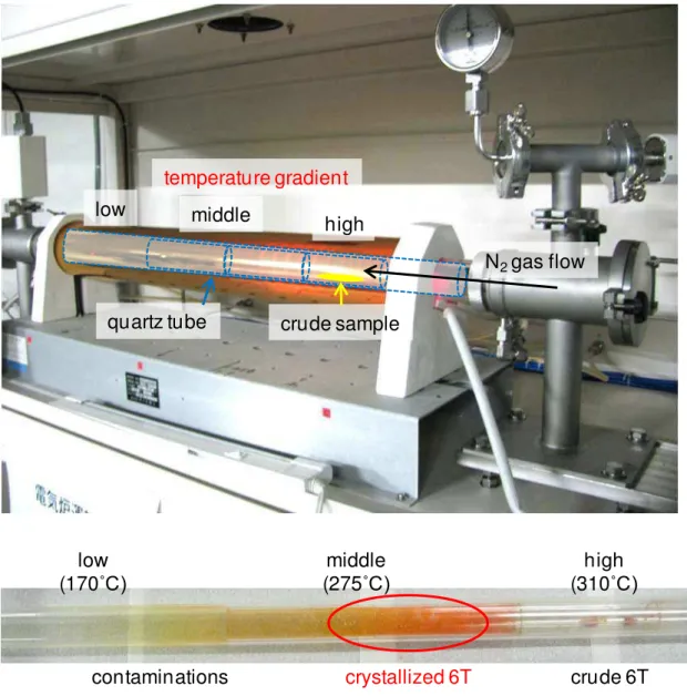
Fullerene (C60) (Frontier Carbon, nanom purple TL) and α-sexithiophene (6T) (Tokyo Chemical Industry) samples were purified by single-crystal sublimation1,2) under flowing N2 at 1 atm and 0.1 atm, respectively. The author used a custom-designed purification system (Epi Tech Inc.) equipped with a three-zone infrared heating furnace (Thermo Riko, GFB 460-3Z) (Fig. 2.1) and grew millimeter-scale crystals (Fig. 2.2). Bathocuproine (Dojindo Laboratories, sublimated), molybdenum oxide (MoO3) (Alfa Aeser, 99.9995%) and cesium carbonate (Cs2CO3) (Sigma-Aldrich, 99.995%) were used without further purification. Ag (Nacalai Tesque, 99.99%) was used for the electrodes.
22
Fig. 2.1 Purification of a 6T sample using a single crystal sublimation system equipped with a three-zone heating furnace.
temperature gradient
N2gas flow middle high
low
quartz tube crude sample
crude 6T contaminations
high (310˚C) middle
(275˚C) low
(170˚C)
crystallized 6T
23
Fig. 2.2 Purified organic semiconductors.
2.2. Fabrication of Cells
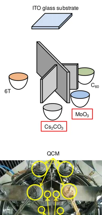
A process chart of the cell fabrication is shown in Fig. 2.3. Indium tin oxide (ITO) coated glass substrates (Sanyo Vacuum Industries) (Fig. 2.3 (a)) were washed three times with water (10 min), methanol (10 min), and acetone (10 min), respectively in an ultrasonic bath. All of the films were deposited by vacuum evaporation onto ITO glass substrates at 10-4 Pa using an oil-free vacuum evaporator (Epi Tech Inc., ET300-6E-HK) (Fig. 2.4). The film thicknesses were monitored simultaneously with the deposition using quartz crystal microbalances (QCM). The film thicknesses monitored by the QCM were calibrated using a surface profilometer (Dektak) (Fig. 2.5). For fabricating a co-deposited film consisting of C60 and 6T (C60:6T) (10:1) (Fig. 2.3 (b)), C60 and 6T were evaporated from two different sources at deposition rates of 0.2 nm s-1 and 0.02 nm s-1, respectively. The cell area onto which the Ag electrode was deposited was defined using a metal mask with an aperture of 0.06 cm-2 (Fig. 2.3 (c)).
α-sexithiophene (6T) fullerene (C60)
24
Fig. 2.3 Process chart of the cell fabrication.
Fig. 2.4 Vacuum evaporator.
Glass ITO Organic
layers Ag Glass
ITO
Glass ITO Organic
layers
(a) ITO glass substrate (b) Deposition of organic layers
(c) Deposition of Ag electrode
vacuum chamber
vacuum pumping system
25
Fig. 2.5 Surface profilometer (Dektak). sample stage
probe
26
2.3. ‘Three Component Co-evaporation’ Technique
Doping into a co-deposited film was performed using a ‘three component co-evaporation’ technique, in which three different evaporation sources were used (Fig. 2.6). Precise monitoring of the deposition rate of the dopant at 1 x 10⁻⁵ nm s-1 was achieved using quartz crystal microbalances (QCM) equipped with a computer monitoring system (ULVAC, Depoview), which allowed us to dope with Cs2CO3 as low as 40 ppm by volume concentration (Fig. 2.7). The distances from the Cs2CO3 source to the QCM and to the substrate were 9 and 18 cm, respectively. The tooling factor as determined by the surface profilometer was 0.25. The relationship between the total-thickness signal from the QCM vs. time was monitored using a PC display. For 40 ppm Cs2CO3, there was a very slow cyclic fluctuation (frequency: ~300 s, amplitude:
~0.05 nm) caused by temperature variations in the coolant water for the QCM. A reproducible increase in the baseline of 0.04 nm, which was only noted during Cs2CO3 evaporation over a prolonged timescale of 3600 seconds, was observed (1 x 10⁻⁵ nm s-1).
27
Fig. 2.6 Equipment for a ‘three component co-evaporation’ technique. ITO glass substrate
6T
C60
Cs2CO3
MoO3
QCM
sources
28
Fig. 2.7 Precise monitoring of deposition rate using a computer monitoring system.
2.4. Measurements of Photovoltaic Properties
The photovoltaic properties of the cells were measured by setting the cells into a sample container equipped with a quartz glass window (Epi Tech Inc.) (Fig. 2.8(a)). The container was evacuated to 10-3 Pa, and the current-voltage (J-V) characteristics and action spectra were measured by irradiating with simulated solar light (Yamashita Denso, YSS-50A) (AM1.5, 100 mW cm-2) (Fig. 2.9), and with monochromatic light from a Xe-lamp (Shimadzu, SPG-3ST) through a monochromator (Fig. 2.10), respectively. The photo-irradiated cell area was precisely defined using a metal mask with an aperture of 0.04 cm-2 (Fig. 2.8(b)).
0 0.02 0.04 0.06 0.08 0.1 0.12 0.14
0 1000 2000 3000 4000
Film thickness / nm
Time / s 1 x 10⁻⁵nm s-1
29
(a) Sample container with a quartz glass window.
(b) Metal mask with an aperture of 0.04 cm-2.
Fig. 2.8 Instruments for the measurement of the photovoltaic properties of the cells.
quartz glass window
photo-irradiated cell area
30
Fig. 2.9 Irradiation of simulated solar light to the cell.
Fig. 2.10 Irradiation of monochromatic light to the cell. monochromatic light
(λ= 450 nm)
31
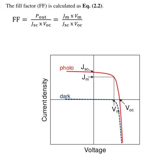
Fig. 2.11 shows the typical current-voltage (J-V) characteristics in the dark and under irradiation with simulated solar light. Various parameters, including the short-circuit photocurrent density (Jsc), the open-circuit voltage (Voc), and the values of current and voltage (Jm and Vm) for the maximum power output (Pout) are also shown. The power conversion efficiency (p) is calculated using Eq. (2.1).
(2.1)
Here, Pin is the incident light intensity. Typically, AM 1.5G (100 mW cm-2) is used for Pin. The fill factor (FF) is calculated as Eq. (2.2).
(2.2)
Fig. 2.11 Typical current-voltage (J-V) characteristics of a cell.
Voltage
C u rr e n t d e n s ity
V
ocJ
scphoto
dark
J
mV
m32
2.5. Kelvin Probe Measurements
The Fermi levels (EF) of the organic films were measured using a Kelvin vibrating capacitor apparatus (Riken-Keiki, FAC-1) (Fig. 2.12).3,4) Both the vacuum evaporator and the Kelvin probe were built into a glove-box (Miwa, DBO-1.5) (Fig. 2.13(a)) that was purged with N2 gas. The concentrations of H2O and O2 were kept below 0.5 and 0.2 ppm, respectively. Thus, during the film deposition and EF
measurements, the films were not exposed to air at any time.
Fig. 2.12 Glove box with a built-in vacuum evaporator.
33
Fig. 2.13 (a) Kelvin vibrating capacitor apparatus (Kelvin probe).
(b) Schematic diagram of the Kelvin probe method.
Fig. 2.13 (b) shows a schematic diagram of the Kelvin probe method. When a capacitor with a capacitance (C) is formed by an Au plate and an organic film that have work functions of ΦAu and ΦS, respectively, a charge (Q) (Eq. 2.3) is induced on the conductive plates due to the difference in contact potentials (ΦAu‒ ΦS).
Q = C(ΦS− ΦAu) (2.3)
When the capacitance is varied (∆C) by vibrating the Au plate, the charge also varies Organic film deposited
on ITO substrate
Au plate
+ +
+
+
Au plate
Vibration
- -
- -
Organic film
Ammeter
V
Ecapacitance
34 (Eq. 2.4) and an alternating current is generated.
ΔQ = ΔC(ΦS− ΦAu) (2.4)
Here, ∆Q and ∆C are the charge difference and the capacitance difference, respectively. Moreover, in the case of applying an external voltage (VE) to the capacitor, the charge difference (∆Q’) is represented by Eq. 2.5.
ΔQ′ = ΔC(ΦS− ΦAu+ VE) (2.5)
By applying VE to the offset ∆Q’, ΦS can be determined by Eq.2.6.
ΦS =ΦAu− VE(ΔQ = 0) (2.6)
Since the value of ΦAu can be measured by x-ray photoelectron spectroscopy,5) ΦS is determined by the value of VE (∆Q’ = 0).
2.6. Energy Band Mapping of Doped Junctions
Energy-band mapping of the doped junctions was performed using a Kelvin probe.6) Fig. 2.14 shows the principle of mapping of a Schottky junction between ITO and a p-type doped organic film. When the organic film is placed in contact with an ITO substrate, the EF of the film agrees with that of the ITO. As a result, the vacuum level (Ev) in the p-type film bends and a depletion layer appears at the ITO/organic layer interface (Fig. 2.14, red shaded region). In the depletion layer, the work function of the p-type film, which is defined by the energy difference between the Ev and EF of the film (EFS), shifts along with the band-bending. Therefore, when Kelvin probe measurements for different thicknesses of p-type films are employed, a shift in the work function, which represents the band-bending in the depletion layer, is observed. Thus, the energy band diagrams of p-type Schottky junctions can be depicted based on the
35
Kelvin probe measurements. This method can be also applied to energy mapping of homojunctions formed in organic films.
Fig. 2.14 Principle of energy-band mapping of doped junctions using a Kelvin probe. An example of a Schottky junction between ITO and a p-doped film is shown.
EV 0 eV
EF 4.7 eV
ITO VB
CB
5 nm
p-doped film ITO
ITO ITO
20 nm
ITO 50 nm
Φ
s= E
V- E
Fs36
2.7. References
1) M. Hiramoto and K. Sakai, Mol. Cryst. Liq. Cryst., 491, 284 (2008).
2) R. A. Laudise, Ch. Kloc, P. G. Simpkins, and T. Siegrist, J. Cyrstal Growth, 187, 449 (1998).
3) M. Hiramoto, K. Ihara, and M. Yokoyama, Jpn. J. Appl. Phys. 1, 34, 3803 (1995). 4) M. Pfeiffer, K. Leo, and N. Karl, J. Appl. Phys., 80, 6880 (1996).
5) H. B. Michaelson, J. Appl. Phys., 48, 4729 (1977).
6) N. Hayashi, H. Ishii, Y. Ouchi, and K. Seki, J. Appl. Phys. 92, 3784 (2002).
37
Chapter 3:
Function Control of pn-Homojunctions and the Formation of
Tandem Photovoltaic Cells in Single Fullerene Films
“Tandem photovoltaic cells formed in single fullerene films by impurity doping”, Norihiro Ishiyama, Masayuki Kubo, Toshihiko Kaji, and Masahiro Hiramoto, Appl. Phys. Lett., 101, 233303 (2012).
Abstract
Tandem photovoltaic cells were formed in single fullerene films by doping with molybdenum oxide and cesium carbonate. A heavily doped n+p+-homojunction acted as an ohmic interlayer between the two pn-homojunction cells. The observed photovoltaic properties of the tandem cell were shown to be consistent with the energy band diagram mapped using a Kelvin probe.
38
3.1. Introduction
Controlling the pn-properties is fundamental to the construction of small-molecular-type organic photovoltaic cells1-7) as well as inorganic ones.8) Recently, the complete control of the pn-properties and the formation of a pn-homojunction in fullerene (C60) 9,10) were reported. In addition, doubling the open-circuit photovoltage (Voc) by use of an organic tandem cell has attracted the attention of many researchers. Organic tandem cell research started in 1990 when Au nanoparticles were incorporated to connect two unit cells together.11) Since then, other materials such as metal clusters and metal oxides have been used for ohmic interlayers.12-14) As for inorganic photovoltaic cells, such as amorphous Si and GaAs cells, p+n+-tunneling ohmic junctions consisting of heavily doped pairs of semiconductors are generally used to connect pn- or pin-cells.15-17) Recently, Timmreck et al. used a heavily doped organic pn-heterojunction as an ohmic interlayer.18) In this study, the author chose C60 as a typical photovoltaic organic semiconductor and attempted to incorporate a tandem photovoltaic cell in single C60 films by doping only. For the ohmic interlayer, a heavily doped p+n+-C60
homojunction was used. For the unit cells, pn-C60 homojunction cells were used.10) Molybdenum oxide (MoO3)9,10) and cesium carbonate (Cs2CO3)19-21) were used as acceptor and donor dopants, respectively.
In this chapter, the author describes a tandem photovoltaic cell built into a single C60 film fabricated by doping only.
39
3.2. Experimental
C60 (Frontier Carbon, nanom purple TL) purified by single-crystal sublimation6,22) was used. MoO3 (Alfa Aeser, 99.9995%) and Cs2CO3 (Sigma-Aldrich, 99.995%) without further purification were used for the acceptor and donor dopants, respectively. Fig. 3.1(a) shows the structure of a tandem cell consisting of two pn-C60 unit cells (Fig. 3.1(b)). The C60 film was vacuum deposited on an indium tin oxide (ITO) substrate which was not exposed to oxygen plasma. Doping with MoO3 and Cs2CO3 was performed by co-evaporation at 10-4 Pa in an oil-free vacuum evaporator (EpiTech Inc., ET300-6E-HK). Precise monitoring of the deposition rates of the dopants was achieved using quartz crystal microbalances equipped with a computer monitoring system (ULVAC, Depoview). To fabricate the pn-homojunctions, MoO3 and Cs2CO3 dopants in volume concentrations of 3,000 (±200) and 500 (±20) ppm, respectively, were used. To make the n+p+-homojunction, both doping concentrations were increased to 50,000 ppm. Ohmic contacts to the ITO and Ag electrodes were formed by heavily doping 10 nm thick layers adjacent to the electrodes with MoO3 (50,000 ppm) for the p+ contact and Cs2CO3 (10,000 ppm) for the n+ contact, respectively.21) The Fermi levels (EF) of the C60 film were measured using Kelvin vibrating capacitor apparatus (Riken-Keiki, FAC-1) without exposure to air at any time.
40
Fig. 3.1 (a) Structure of a tandem cell incorporating two pn-homojunction C60 cells connected by an n+p+-homojunction. (b) Structure of a unit cell incorporating a pn-homojunction.
(b)
(a)
p-C60 100 nm
n-C60 100 nm
p-C60 100 nm
n-C60 100 nm
ITO Ag
Cs2CO3-doped (50,000 ppm)
n+-C60 5 nm
MoO3-doped (50,000 ppm)
p+-C60 15 nm
MoO3-doped (50,000 ppm)
p+-C60 10 nm
Cs2CO3-doped (10,000 ppm)
n+-C60 10 nm MoO3-doped
(3,000 ppm)
Cs2CO3-doped (500 ppm)
p-C60 100 nm
n-C60 100 nm
ITO Ag
MoO3-doped (50,000 ppm)
p+-C60 10 nm
Cs2CO3-doped (10,000 ppm)
n+-C60 10 nm
41
3.3. Results and Discussion
3.3.1. Exploration of a Donor dopant
Since the aim of this thesis is the development of doping techniques for co-deposited films, the author searched for a donor dopant so that it can be applied to a co-deposited film consisting C60 and α-sexithiophene (6T). The donor dopant was explored among various materials, which can be deposited by vacuum evaporation. Lithium encapsulated fullerene (Li@C60),23,24) lithium fluoride (LiF),25) ruthenium oxide (RuOx), Calcium (Ca)10) and Cs2CO3 (Table 3.1) were tested. For Li@C60-doped, LiF-doped and RuOx-doped C60 films, the EFs were not changed from the original EF position of C60 (Fig. 3.2(a)). In contrast, for Ca-doped and Cs2CO3-doped C60 films, the EFs shifted negatively (Fig. 3.2(b) and 3.2(c)). These results mean that Ca and Cs2CO3 act as the donor dopants making C60 n-type. Actually, both Ca-doped and Cs2CO3-doped C60 films acted as n-type layers in pn-homojunctions formed in C60 films. However, for Ca-doped 6T film, 6T was decomposed to another material which gave out a sulfurous smell. On the other hand, for Cs2CO3-doped 6T films, there was no sign that 6T was decomposed. Thus, the author adopted Cs2CO3 as the donor dopant.
42
Table 3.1 Effect of doping with various materials. Dopant Shift in Fermi level
of C60by doping
Remarks
Li@C60 No Shift
LiF No Shift
RuOx No Shift
Ca Negative Shift 6T was decomposed by doping with Ca.
Cs2CO3 Negative Shift Both C60and 6T were not decomposed by doping with Cs2CO3.
43
Fig. 3.2 Energy diagram of C60 for non-doped (a), Ca-doped (b) and Cs2CO3-doped films. The position of the upper edge of the valence band (VB) and the lower edge of the conduction band (CB) of C60 are determined by photoelectron spectroscopy and inverse photoelectron spectroscopy, respectively.
3.0
4.0
5.0
E lect ro n en er g y / eV
6.07.0
4.60
VB (6.4) CB (4.0)
(a) non-doped C60
4.49
(b) Ca-doped C60
4.38 E
F
(c) Cs2CO3-doped C60
44
3.3.2. Control of Fermi Levels in Single C60 Films by Doping with MoO3 and Cs2CO3
Fig. 3.3 shows the energy band diagrams of C60 films doped with MoO3 and Cs2CO3. The values of the work functions of ITO, Ag, MoO3, and Cs2CO3 films are also shown. For the 500 ppm Cs2CO3-doped C60 film, the EF is located at 4.38 eV, which is close to the lower edge of the conduction band (CB) of C60 (4.0 eV).26) A thick co-deposited film of C60:Cs2CO3 in the ratio 10:1 changed the color to reddish brown and showed a new broad charge transfer (CT) absorption from the visible to the near infrared region. Since the work function of Cs2CO3 (2.96 eV) is more negative than the conduction band of C60 (4.0 eV), it is reasonable that Cs2CO3 donates an electron to C60 and forms a CT complex, i.e., C60----Cs2CO3+. Here, the positive charge on the Cs2CO3+ group can be regarded as a spatially fixed positive ion, i.e., an ionized donor. The negative charge on C60 can be liberated by thermal energy and acts as a free electron in the conduction band of C60. Thus, the author concludes that Cs2CO3 acts as a donor dopant making C60 n-type. This donor property did not disappear even after exposure to air. When the doping concentration was increased to 50,000 ppm, EF shifted slightly more negative (4.35 eV). On the other hand, for 3,000 and 50,000 ppm MoO3-doped C60 films, the EFs are located at 5.88 and 5.97 eV, respectively, which are close to the upper edge of the valence band (VB) of C60 (6.4 eV). Formation of p-C60 by MoO3 doping is caused by the opposite mechanism to Cs2CO3 doping.9)
45
Fig. 3.3 Energy diagram of C60 films doped with MoO3 and Cs2CO3. Values of the work functions of ITO, Ag, MoO3, and Cs2CO3 are also shown.
3.0
4.0
5.0
Electron energy / eV 6.0
7.0
EF(3,000 ppm)
Ag 4.13 Cs2CO3
2.96
EF(50,000 ppm)
MoO3 6.69 ITO
4.70 EF(500 ppm)
4.35 4.38 4.0 (CB)
6.4 (VB) 5.88 5.97 MoO3- doped C60
Cs2CO3- doped
C60
EF(50,000 ppm)
46
3.3.3. n+p+-C60 Homojunction Acting as an Ohmic Interlayer
Curves A and B in Fig. 3.4 show the current-voltage (J-V) characteristics for a tandem cell (Fig. 3.4(a)) and a unit cell (Fig. 3.1(b)), respectively. For the tandem cell, the Voc value reaches 1.90 V. For the unit cell, the Voc value is 1.03 V. Voc has almost doubled (84% increase) by connecting two unit cells. When the n+p+-homojunction between the two unit cells of the tandem cell (Fig. 3.1(a)) was
removed, Voc remained the same (1.03 V), but the photocurrent density decreased significantly (curve C) compared to the unit cell (curve B). Thus, an n+p+-interconnecting homojunction is indispensable for doubling the Voc value.
The short-circuit photocurrent density (Jsc) of the tandem cell was about a third of that of the unit cell since the magnitude of the photocurrent of the tandem cell was limited by the back cell operating under the light attenuated by the front cell. To overcome this, the values of Jsc generated by front and back cells should be equalized by equalizing the light absorption of the front and back cells having optimized thicknesses.
47
Fig. 3.4 Current-voltage (J-V) characteristics for the tandem cell (curves A)(Fig. 3.1(a)) and the unit cell (curves B)(Fig. 3.1(b)). Curves C are for a tandem cell without an n+p+-interconnecting homojunction. The photo and dark currents are shown by solid and broken curves, respectively. The ITO electrode was irradiated with simulated solar light (AM1.5, 100 mWcm-2). Measurements were performed at 10-3 Pa. The short-circuit photocurrent, open-circuit photovoltage (Voc), fill factor, and efficiency of the cells: (A) 0.09 mAcm-2, 1.90 V, 0.29, 0.05%. (B) 0.29 mAcm-2, 1.03 V, 0.34, 0.10%. (C) 0.06 mAcm-2, 1.03 V, 0.32, 0.02%.
-0.1 0 0.1 0.2 0.3 0.4 0.5
-0.5 0 0.5 1 1.5 2 2.5
Current density / mA cm-2
Voltage / V
B
C A
48
3.3.4. Energy Band Diagram of a Tandem C60 Photovoltaic Cell
In order to clarify the operating mechanism, energy band mapping of pn-homojunctions was performed using a Kelvin probe.27,28) The positions of EF for different film thicknesses near the pn-homojunction were measured from both sides of the junction interface. That is, the positions of EF of Cs2CO3-doped C60 films deposited on MoO3-doped C60 films (Fig. 3.5(a)) and also those of MoO3-doped films deposited on Cs2CO3-doped films (Fig. 3.5(b)) were measured. The blue curves A in Figs. 3.5(a) and 3.5(b) show the observed EF values for MoO3/Cs2CO3 doped homojunctions with concentrations of 3000/500 ppm, respectively. For the Cs2CO3 doped side (Fig. 3.5(a)), EF gradually shifts more negatively, i.e., EF gradually approaches the original EF position of 500 ppm Cs2CO3-doped C60 (4.38 eV, see Fig. 3.3). This gradual shift extends beyond 100 nm. On the contrary, for the MoO3-doped side (Fig. 3.5(b)), EF gradually shifts more positively, i.e., EF gradually approaches the original EF position of 3,000 ppm MoO3-doped C60 (5.88 eV, see Fig. 3.3). This gradual shift ends at around 30 nm. The profiles of the potential of the depletion layers formed on both sides of the homojunction can be depicted directly from the above complementary EF observations.29) Obviously, pn-homojunctions are drawn here (Fig. 3.6, blue shaded regions).
On the other hand, in the case of a heavily-doped homojunction, a narrower depletion layer is observed. The red curves B in Figs. 3.5(a) and 3.5(b) show the observed EF values for a MoO3/Cs2CO3 homojunction doped with concentrations of 50,000/50,000 ppm. For the Cs2CO3 doped side (Fig. 3.5(a)), a rapid negative shift of EF over the first 5 nm before reaching the original Fermi level position of 50,000 ppm Cs2CO3-doped C60 (4.35 eV, see Fig. 3.3) can be seen. For the MoO3-doped side (Fig.