Implementing a Built-In
Self-Test PLA Design
By
achieving
highfault
coverage atlowoverhead,
this design scheme offersapractical
solution to the PLAtesting problem.
Robert Treuer, Hideo
Fujiwara, and
VinodK.Agarwal
McGill University
Programmable logic arrays pres- ently occupyanextremely impor- tant role as digital subsystems, par- ticularly in the design ofcomplexVLSI chips. Atypical large PLAmayhave as many as 50inputs, 67 outputs, and 190 product terms (see Law and Shoji,' for example). The testing of such PLAs thus becomes a rather dif- ficult problem. However, due to the structuralregularity ofPLAs,thistest problem has attractedtremendousat- tention in recent years. In particular, the design of built-in self-test PLAs with very low overhead and very high fault coverage appears to beapossible solution to the testing problem.2 In this article we briefly summarize the proposals made in this direction. We thenprovide implementation details of a newapproach thatrequireslessover- head than all other existing designs. This approach offers a proven fault coverage of allsinglefaultsandalmost all multiple faults.
The most critical requirement for designing a BISTPLAis that thetest
patterns used to test the PLA and the output response generated by these tests be independent of the function realizedby the PLAundertest. More- over,tokeep overheadto aminimum, the test patterns should be generatable bya very simple circuit and in a rea- sonable amount of time, and the out- put response should be compressible intoasmall number of bits. Finally, in addition to functional independence, simple testgeneration,and significant compression of the output response, the fault coverage of both the original PLA and theadditional test circuitry should be acceptable. An excellent theoretical, but impractical, solution can be made available to fully satisfy anyrequirements that are not met, but all four requirements must be met in thedesignofapractical BIST PLA.
The fault coverage required for PLAs must include stuck faults, bridg- ing faults, and crosspoint faults. The crosspoint faultisuniquetoPLAsand is caused by theunintentionalpresence orabsence of devices (that is, transis- tors for PLA programming) in the AND and OR arrays of the PLA. OstapkoandHong3 andSmith4have shown that a complete test set to detect all single crosspoint faults in a PLA also detects most of the single stuck and bridging faultsas well. It has also been established that such a test set detects most (over98percent) multiple
Hideo Fujiwarawas avisitingprofessoratMcGllI
Universitywhilethisresearch wascarriedout. He is now with the DepartmentofElectronicsand
CommunicationsatMeijiUniversityin Japan.
0740-7475/85/0400-0037$01.00 © 1985 IEEE 37
April1985
vQ',
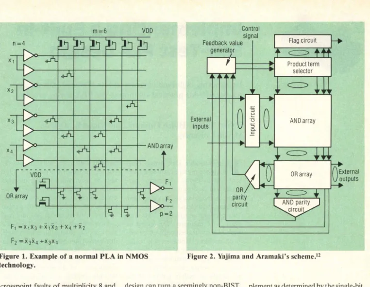
Figure 1. Exampleof anormal PLA inNMOS
technology. Figure 2. Yajima and Aramaki's
scheme.'2
crosspointfaults ofmultiplicity 8and less.5 Rajski and Tyszer6 improved upon these results, establishing the sufficiency of the single crosspoint fault test set for all faults of interest. Nonetheless, this conclusion is not veryuseful for BIST PLAs, since these results do not apply to the situation when the output response is com-
pressedintoafew bits.
Another interesting aspect of de- signing BIST PLAs is theestimationof the overhead for additional circuitry. It is well known that the routing of signals often takes more silicon area than the processing components (see Mead andConway7).Thus,anycalcu- lations madeto estimate the overhead without considering the routing area are often toooptimistic. Inparticular, a largenumber of so-called easilytest- able PLA designs (see Rajski and Tyszer8 for a comparison of various known schemes) are not necessarily suitable candidates for BIST PLAs unless proper estimates areobtained. In some cases, of course, an ingenius
design can turn a seemingly non-BIST approach into a BIST approach (for example, the design described by Hua etal.).
Finally, since different schemes use different numbers of test patterns and different hardware designs, another useful parameter to consider in BIST design is the delay per test pattern application. It iscalculated on the as- sumption that the PLA input de- coders, the AND array, and the OR array each have one gate delay. Each exclusive-OR gate is assumed to have two gate delays. Thus, for instance, a parity cascadeon mproduct linesof a PLA will result in a test delay of 2m units (see Hassan and
McCluskey'0).
Review
of BIST PLAdesignsA PLA, as shown in Figure 1, basically consists of two arrays of or- thogonally crossing lines. The top ar- ray, often referred to as the AND ar- ray, has 2n bit lines as rows and m product lines as columns. Every bit line carries an input signal or its com-
plement as
determined
bythesingle-bit
decoders at the left ends of the rows.It is also possible to have double-bit decoders,I in which case two input signalsaredecoded into four bit lines, eachcarryingaunique minterm of the two variables. In this article, we con- sider only single-bit decoder PLAs because the extension to double-bit decoders is straightforward. Each product line is formed by a logical NOR operation on some selected bit lines. The selection of each bit line is made by means of a transistor placed at the intersection of the correspond- ingbit line andproduct line, asseenin Figure 1. The bottom array, called the OR array, consists ofmproduct lines as columns and p output lines (also called sum lines) as rows. Hereagain, each output line forms a logical NOR ofcertain product lines by means of transistors placed at the appropriate intersections. Thus, each output line corresponds to the output of a two- levelNOR-NOR logic circuit.It iswell known that any sum-of-products ex-
pression canbe realized by suchacir- cuit, provided that the inputsandout- puts are complemented as shown in Figure 1.
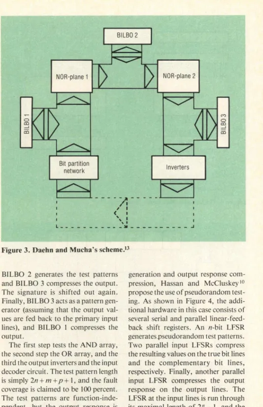
In oneofthe first reported designs of BIST PLAs, Yajima and Ara- maki12 proposedthestructureshown in Figure 2. The additional com- ponentsin thisdesignarefourproduct lines, two output lines, an (m+4)-bit shift register,aparity circuit form+2 product lines, another parity circuit forp+2 outputlines,amodifiedinput decoder with an n-bit shift register, andasimple feedback valuegenerator. Inthetestmode,themodified decoder and the (m+4)-bit shift registergener- ate a test pattern every clock cycle, which, when applied to thePLA, re- sults in the output oftwo parity sig- nals. These two parity signals, along with the twoproduct signals shown in Figure 2, are used by the feedback value generator to help generate the next test pattern.Aftertheapplication of n+2m +8 test patterns, the com- pressedoutput responseis available in the (m+4)-bit shift register. If this response matches the fault-free com- pressed response, then the PLA is declaredtohave nofaults.
The fault coverage of this scheme consists of all single crosspoint faults, all singlestuck faultsinthe twoparity circuits, andall faults in the modified decoder and the (m + 4)-bit shift reg- ister. No multiple faults are guar- anteed to be covered. The delay per testis2m + 7.
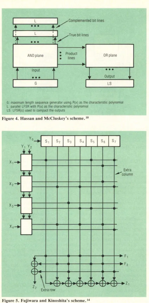
Using a completely different ap- proach published at about the same timeasthe abovescheme, Daehn and Mucha13 proposed the use of non- linear-feedback shift registers both as pattern generators and as output response compressors for BIST PLA design. Such registers are basically a modified form of what is known as a built-in logic block observer, or BILBO. As shown in Figure 3, the schemeteststhe PLA in three steps. In the first step, test patterns are gen- erated by BILBO I and the output response is compressed by BILBO 2. Theresulting signature is then shifted out for inspection. In thesecond step,
Figure3.Daehn and Mucha'sscheme.13 BILBO 2 generates the test patterns and BILBO 3 compressestheoutput. The signature is shifted out again. Finally, BILBO 3 acts as a pattern gen- erator (assuming that theoutput val- ues are fed back to theprimary input lines), and BILBO I compresses the output.
Thefirst step tests the AND array, thesecond step the OR array, and the third theoutputinverters and the input decodercircuit. The test patternlength is simply 2n + m +p +1, and thefault coverage is claimed to be 100 percent. The test patterns are function-inde- pendent, but the output response is not. The actual overhead of the scheme is limited by the three BILBOs, which occupy a reasonably large area. More- over, the need to store on-chip three different fault-free signatures and the facility that compares them can take up significant area. The main advan- tage of this scheme lies in its simplicity, its linear test length, and its delay per test, which is five units.
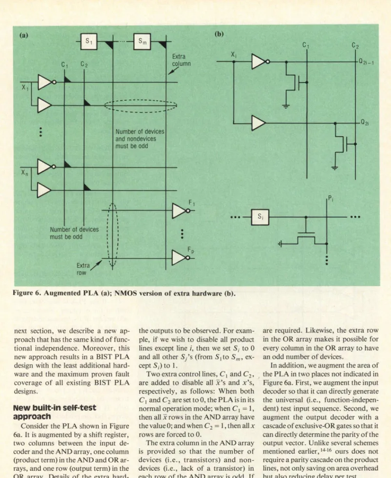
In a scheme that employs linear- feedback shift registers for pattern
generation andoutput response com- pression, Hassan and McCluskey' propose the use ofpseudorandomtest- ing. As shown in Figure 4, the addi- tionalhardware in thiscaseconsists of several serial and parallel linear-feed- back shift registers. An n-bit LFSR generatespseudorandomtestpatterns. Two parallel input LFSRs compress theresulting valuesonthetruebit lines and the complementary bit lines, respectively. Finally, another parallel input LFSR compresses the output response on the output lines. The LFSRat the input lines is run through its maximal lengthof2n- 1, and the threecompressed signatures are com- pared withthe fault-free signatures to determineif the PLA is faulty or not. If the feedback polynomials for all four LFSRs are identical, then the following fault coverage can be en- sureddespite the random testing pro- cedure: all multiple-bit-line stuck faults, all output faults, and most (in theprobabilistic sense)ofthe product- linestuck and missing-device faults in the AND array.
Figure 4. Hassan andMcCluskey'sscheme.'0
Extra
colum
Figure 5. Fujiwara and Kinoshita's scheme.14
This scheme, like the others, does not provide a function-independent compressed output. Moreover, dueto the needtoapply 2n-I testpatterns, the scheme is suitable only for PLAs with a small number of input lines. Thedelayper testis six units. Theover- head might be minimized if system latches could be used as linear-feed- backshiftregistersat the time of test- ing. This advantage also applies to Daehnand Mucha's scheme.
Another class of schemes,all devel- oped for the easily testable design of PLAs, has been proposed as suitable forBIST as well. 9 Asanexample, we consider the scheme suggested by Fu- jiwara and Kinoshita14 (see Figure 5). Here, one additional product line is used, so the number of devices on each bit line is odd. Similarly,anadditional sum line is used, so the number of devices on each column in the ORar- rayis odd. Two parity circuits are used to calculate the parity of the product linesand the output lines foreach test pattern. A shift register activates any one product line and deactivates all otherproduct lines. Finally, the mod- ified input decoders allow any bit line to have avalue that isnot necessarily the complement of itscompanion bit line. The number of test patterns re- quired in this scheme is 2n + 3m, whereas the delay per test is 2m + 3 units. The fault coverage includes all single stuck faults on the input lines, the output lines, the gates within the decoders, and all lines in the AND and OR arrays, as well as allsingle cross- point faults in the AND and OR ar- rays. Unlike the three schemes de- scribed above, thisone waslaidout in NMOS according to some ingenious design concepts.9 In a later section we will provide some details on this im- plementation.
Other similar schemes, such as those proposed by Saluja et al. 15 and by Hong and Ostapko,'6 may also be considered suitable forBISTdesigns. However, of all the schemes proposed in the literature, only a few, such as Fujiwara and KinoshitaI4 and Hong and Ostapko,16 provide completely function-independent input genera- tion and output compression. In the
Figure 6. Augmented PLA (a); NMOS version of extra hardware (b).
next section, we describe a new ap- proach that has the samekind of func- tional independence. Moreover, this newapproach results in a BIST PLA design withthe least additional hard- ware and the maximum proven fault coverage of all existing BIST PLA designs.
New
built-in self-test
approach
Considerthe PLAshown inFigure 6a. Itisaugmentedby ashift register, two columns between the input de- coder andthe AND array, one column (product term)in theANDand ORar- rays, and one row (output term) in the OR array. Details of the extra hard- ware are shown in Figure 6b.
The added shift register can disable all product lines but one; this allows the effect of a single product line on
the outputs tobe observed. For exam- ple, if we wish to disable all product lines exceptline i, thenwe setSi to 0 and allother
Sj's
(fromSIto
Sm,ex- ceptSi)
to 1.Two extracontrollines, C1 andC2, are added to disable all x's and x's, respectively, as follows: When both ClandC2are set to0,the PLAisinits normaloperation mode;whenCl=1, then allx rowsin theANDarrayhave thevalue0; and when C2=1,thenallx rows areforcedto0.
The extra column in the AND array is provided so that the number of devices (i.e., transistors) and non- devices (i.e., lack of a transistor) in each rowof the AND array is odd. If theoriginal number of product lines is odd, then one extra column (i.e., total miseven) can ensure therequired odd parity; otherwise, two extra columns
are required. Likewise, theextra row in the OR arraymakesit possiblefor everycolumn in theOR arraytohave anodd number of devices.
Inaddition, we augment the area of thePLAintwoplacesnotindicatedin Figure6a.First,weaugment theinput decodersothatitcandirectlygenerate the universal (i.e., function-indepen- dent) testinput sequence. Second, we augment the output decoder with a cascade of exclusive-ORgates so thatit candirectly determine the parity ofthe output vector. Unlike several schemes mentioned earlier,14-16 ours does not require aparity cascade on the product lines, notonly saving on area overhead butalso reducing delay per test.
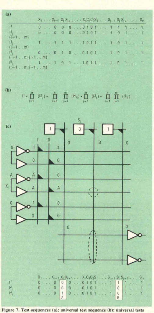
Testing scheme. Thetesting scheme usedon theaugmentedPLA is asfol- lows:First, we apply the test sequences
Figure 7.Test sequences (a); universal testsequence (b); universal tests 1I, J2j,J4.. (C).
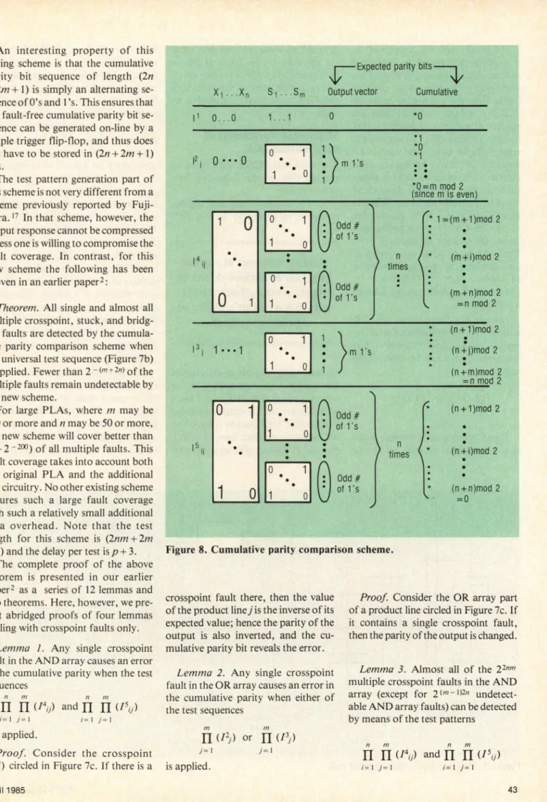
showninFigure7ain the order shown in Figure 7b, the universal test se- quence. Wecompress everynew out- put vectorintoasingleparity bit,and then we exclusive-OR this bit withabit representing the cumulative parity of all previous output vectors to obtain the newcumulative parity bit. Byex- amining the cumulative parity bit at only2n + 2m + 1specifictimes,wecan detect all single faults and almost all multiple faults. Full details are pro- videdbelow.
Definition. Letthetermcumulative parity comparison refer to the com- parison scheme (see Figure 8) of the cumulative parity bit responsestothe universaltest sequence.
Theasterisks inFigure8indicate the (2n+2m +1)times when the cumula- tive parity bit is compared to its ex- pected value. Note that the cumulative paritycomparison scheme isfunction- independent (i.e., validfor allPLAs). 2 Theexpected parity bits of individual output vectors werederivedasfollows (usingFigure7c):
IP:If the PLA isfault-free,then the output vector isastring of 0's whose parity is0.
12j:
If the PLA is fault-free, then each of the m output vectors has an odd number of I's, because each prod- uct line in the OR array has anodd numberofdevices.Thus, the parity of each output vector is I (similarly for I3).I4ij:
Assume the PLA to be fault- free. Forsimplicity, consider the par- tial test patternJ4j;
where i is a constant and forj= I to m, whichac- tivates the crosspoints on bit linexi
only. If the crosspoint (xj,j) has a device,then theproduct linejispulled down to0, whichproduces an output of all0'sand thus aparity bit of 0. If the crosspoint (xj,j) has no device, thenthe productlinej stays at1,which producesan output with an odd num- ber of l's and thus a parity bit of 1. RecallfromFigure 6a thatthe number of nondevices ofeach product line is odd; therefore, an odd number of parity bitsof I is created for each bit line(similarly for15jj) .An interesting property of this testing scheme is that the cumulative parity bit sequence of length (2n +2m+1) is simplyan alternating se- quenceof 0's and I's.This ensuresthat thefault-free cumulative parity bitse- quence can begenerated on-line bya simple trigger flip-flop, and thus does not have to be stored in (2n+ 2m + 1) bits.
The test pattern generation part of this scheme isnot verydifferent froma scheme previously reported by Fuji- wara.17 Inthat scheme, however, the outputresponsecannotbecompressed unlessoneis willing to compromise the fault coverage. In contrast, for this new scheme the following has been proven inanearlierpaper2:
Theorem. All single and almost all mnultiple crosspoint, stuck, and bridg- ing faults are detected by the cumula- tive parity comparison scheme when theuniversaltest sequence(Figure 7b) is applied. Fewer than 2-(m+2n)of the multiple faults remain undetectable by thenewscheme.
For large PLAs, where m may be 100 or more and n may be 50 or more, thenewscheme willcover better than (I -2-2) of all multiple faults. This faultcoverage takes into account both the original PLA and the additional testcircuitry. No other existing scheme ensures such a large fault coverage with such a relatively small additional area overhead. Note that the test length for this scheme is (2nm + 2m
+I)and the delay per test is p+3. The complete proof of the above theorem is presented in our earlier paper2 as a series of 12 lemmas and twotheorems. Here, however, we pre- sent abridged proofs of four lemmas dealing with crosspoint faults only.
Lemma 1. Any single crosspoint fault in the AND array causes an error in thecumulative parity when the test sequences
n m n in
H
rH (I4ij)
andII II (I5ij)
i=1 j= i=- j=I
are applied.
Proof. Consider the crosspoint (i,j) circled in Figure 7c. Ifthereis a
E~~cpecte~~~~$ r4
2' ). <
4' 0. .0 V. .1
2 .' . *1
I
0 1
0
1 0
*,, a f W*S ; SE i;
I0 1 ;}} }0;;1
I . I-: 'i100 10
. 0 d I
.
;,.,-!.::
ofl'-s;::.s:
*
p
f.m*sR *
(n+i.niod 2
.w44.iflod 2 (n +r9mod 2
Figure 8. Cumulative parity comparison scheme.
crosspoint fault there, then the value of theproduct linejis the inverse of its expectedvalue; hence theparityof the output is also inverted, and the cu- mulative parity bit reveals theerror.
Lemma 2. Any single crosspoint fault inthe OR array causesan errorin the cumulative parity when either of the testsequences
m m
rIL (12.)
orII (J3i)
j=l j=
isapplied.
Proof. Consider the OR array part ofaproduct line circled in Figure 7c. If it contains a single crosspoint fault, then the parity of the output is changed.
Lemma 3. Almost all of the 22nm multiple crosspoint faults in the AND array (except for 2(m-1)2n undetect- able AND array faults) can be detected by means of the test patterns
n m n m
fI
fl(I4,;)
andI I (15ij)
i=1 j=l ij= j=l
t
Apz4m
.>I"':
iN2 -4i
43
Proof.
I4,j
andYij
activate all m crosspoints of a bit line to produce a newcumulative parity bit;thus, if the total number offaultsonthe same bit line is even, the cumulative parity bit does not indicate a fault, since the numberof devices and nondevices for the line remains odd. Therefore, the only multiple faults that cannot be detected are those having an even number of faults (or no faults at all) on each bit line. The total number of possible multiple crosspoint faults in the AND array is 2(2n)(m).Thenumber ofpossible even faults (including zero faults) for a single bit line is 2(m-'). Thus, the ratio (AND array only) of undetectable faults to thetotal number of faults is (2m-1)2n/22nm=2-2n, which is a very small number for typ- ical values of n.Lemma 4. Almost all of the 2Pm multiplecrosspointfaultsintheOR ar- ray (except for 2(P-)m undetectable OR array faults) can be detected by either
m (=1
or
]I
m(1k3)
j=I
Proof. Analogous to Lemma3,the only multiple faults that cannot be
detected are those withaneven num- ber of faults (or no faults at all) on eachproduct line (OR array part only). Theratio(OR arrayonly) ofundetect- ablefaultstothetotalnumber of faults is(2P-I)m/2Pm=2-m
VLSI
implementation
ofaugmented PLA
The original PLA is augmented by the addition of the following four small circuits:
(1) The product lines' shift register is shown in Figure 9. It is a shift
Adding inverters at regular
intervals minimizes delays in
signal propagation without
reducing a circuit's ability to
determine parity.
register whose number of cells is half thenumber ofproduct lines, as in the scheme proposed by Hua et al.9 Each shift register cell's output (labeled
"Next value" in Figure 9) is shared by two adjacent product lines by multi- plexing. The basic cell's layout (under
Mead and Conway's7 NMOSdesign rules) is 16 lambda wide and 170 lamb- dalong.Multiplexing is used because no morethan oneshift register cellcan be fitted into the narrow 16-lambda width sharedby two product lines.
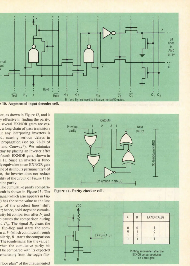
(2) The augmented input decoder is shown in Figure 10. It uses a shift register cell for each pair of com- plementary bit lines. The inverters in the shift register cell have been re- placed by NAND gates to allow the shiftregistertobeinitializedtocertain states.The holdsignalshowninFigure 10is needed to hold the value x in each cell, since shifting occurs only every mth clock cycle, unlike the shift reg- ister of Figure 9,whereshiftingoccurs atevery clock cycle. The output of the shift register cell passes through a multiplexer to the complementary bit lines. The basic cell's layout is 16 lamb- da wide and 175 lambda long-135 lambda longer thantheunaugmented input decoder.
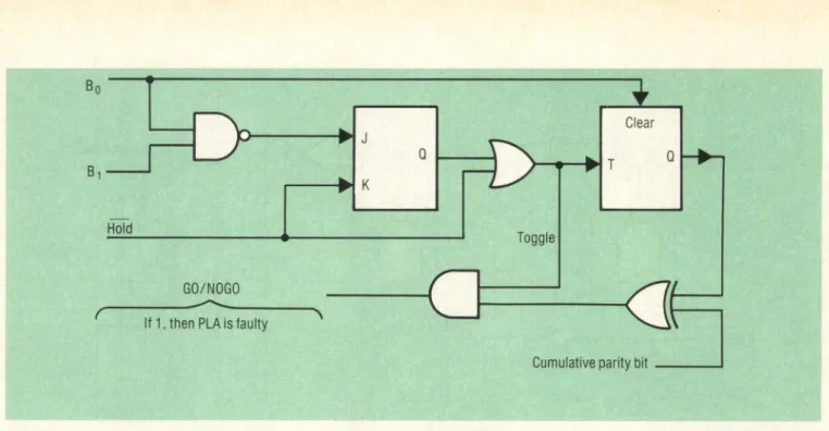
(3) The parity checker placed after the outputdecoderis shown inFigure 11. It uses a chain of exclusive-NOR gates (i.e., an exclusive-OR gate fol- lowed by an inverter) to find the parity of the output vector. An EXNOR gate takes up lesssiliconarea than anEX-
**C * * C S~~~~~~~~~~~~~~~~~~~~~~~~~~,i*Z
C~~~~~~~~~~~~~~~~~~~~~~~~~~~~~~I C~
Figure 9. Product lines' shift register cell.
Test,:
i e'
Figure 10. Augmented input decoder cell. ORgate,asshown inFigure 12,andis
equallyeffective infinding theparity. OtP--s When several EXNOR gates are cas-
caded, alongchain ofpasstransistors prt without any interposing inverters is
created, causing serious delays in signal propagation (see pp. 22-25 of Mead and Conway7). We minimize
this delay byplacing an inverter after every fourth EXNOR gate, shown in Figure 11. Since an inverter is func-I tionally equivalentto an EXNOR gate withoneofitsinputs permanentlytied
to zero, the inverter does not reduce theabilityofthe circuit ofFigure1 1 to
determineparity.
Zl''t,^da
Iti 9'tvtO${(4) The cumulative parity compara-
tor circuit is shown in Figure 13. The Figure 11. Parity checker cell. hold signal (which also appears in Fig-
ure 10)has the same value as the last
cell
Sm,
of the product lines' shift Dregister; hence,holdstopsthecumula- tiveparitybitcomparisonafterI2 and
J3 and causes
~~~~~~~~~~~~~~~~AB
thecomparison during EXNOIJ4j
andI5j.
The signalBo
clears thetoggle flip-flop and starts the com- 0 0 1
parisonatII (whichcontinuesthrough 0 1 0
J2 similarly, B1 startsthe comparison at
,3
Thetoggle signal
hasthevalue i only when the cumulative parity bit should be compared with itsexpected value emanating from the toggle flip-flop.A
BA"floorplan"of theunaugmented
PLA, showing all the dimensions in Figure 12. The EXNORgate.
Figure 13. Cumulativeparity bit comparator. The twoflip-flopsarestandardJ-K and toggleflip-flops(for simplici- ty, their clock and preset inputs are not shown, and only their uninverted outputs are used).
units oflambda, is shown in Figure 14. The total area of the unaugmented PLA is also shown. The circuits de- scribedaboveaddarea asfollows:
(1) The product lines' shift register adds 170x8m=1360m.
(2) The augmented input decoder adds 135 extra x16n=2160n.
(3) The parity checker adds 95x
8p=760p.
(4) The comparator adds a small areathat is independent of the size of the PLA and is thus ignored without any loss ofgenerality.
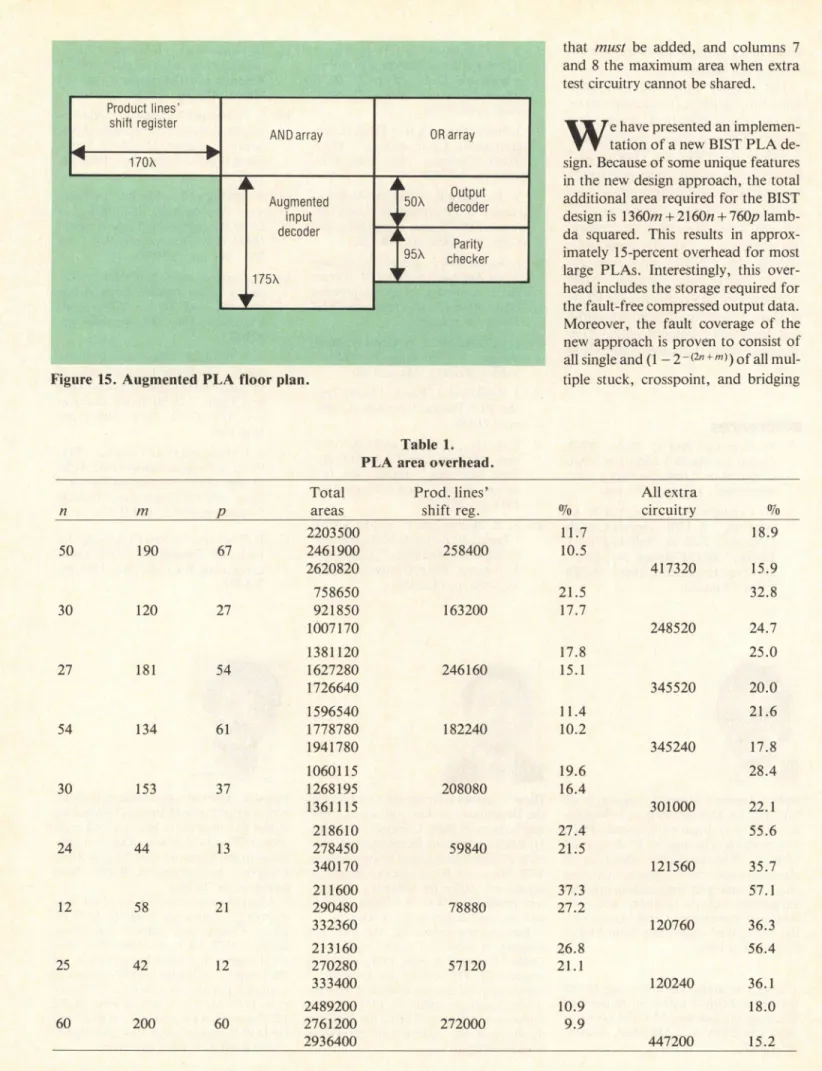
Figure 15 shows the floor plan of the augmented PLA. Thus, the total extra areais 1360m+2160n+760p.
A numerical value for area over- headcanbe obtainedintwoways:
;23<~~~~~~~~
Figure 14.PLAdimensions.
(1) as the ratio (extra area/original area)x 100%or
(2) as theratio (extra area/original plusextraarea)x 100%.
In some recent VLSI chips, PLAs occupy a large fraction of the chip area, as for example AT&T's WE 32000, a 32-bit single-chip micropro- cessorthat haseight PLAs! InTableI we show the areaoverhead(using both ratios) for these eight PLAs and for a 60input, 60 output, 200 product term PLA. Thefirst three columns givethe number of inputs, product terms, and outputs.The fourth column has three values perPLA:the original PLA area (in lambda squared), theoriginalPLA plus the product lines' shift register, and the fully augmented PLA. The fifth and sixth columns give thearea and overhead of the product lines' shiftregister. Theseventh andeighth columnsgivethe areaandoverhead of all three extra circuits. The larger percentage corresponds to ratio I above, the smaller to ratio 2. The reason for giving the overhead when onlytheproduct lines' shift register is added to the PLA is that if several PLAs on achip shareinput and output buses,then theinputpattern generator circuit and the output parity checker circuitcan be shared. Hence, columns 5 and 6 represent the minimum area
Figure 15. Augmented PLA floorplan.
that must be added, and columns 7 and 8 the maximum area whenextra testcircuitrycannot be shared.
],le have presentedanimplemen-
W
T tationofa newBIST PLA de-sign. Becauseofsomeuniquefeatures in thenewdesign approach, the total additionalarea requiredfor the BIST designis 1360m+2160n+760plamb- da squared. This results in approx-
imately 15-percent overhead formost
large PLAs. Interestingly, this over- head includesthestoragerequiredfor the fault-freecompressedoutputdata. Moreover, the fault coverage of the
newapproach is proventoconsist of allsingle and(I-2-(2n+m)) of all mul- tiple stuck, crosspoint, and bridging
Table 1. PLA area overhead.
Total Prod.lines' All extra
n m p areas shift reg. % circuitry °
2203500 11.7 18.9
50 190 67 2461900 258400 10.5
2620820 417320 15.9
758650 21.5 32.8
30 120 27 921850 163200 17.7
1007170 248520 24.7
1381120 17.8 25.0
27 181 54 1627280 246160 15.1
1726640 345520 20.0
1596540 11.4 21.6
54 134 61 1778780 182240 10.2
1941780 345240 17.8
1060115 19.6 28.4
30 153 37 1268195 208080 16.4
1361115 301000 22.1
218610 27.4 55.6
24 44 13 278450 59840 21.5
340170 121560 35.7
211600 37.3 57.1
12 58 21 290480 78880 27.2
332360 120760 36.3
213160 26.8 56.4
25 42 12 270280 57120 21.1
333400 120240 36.1
2489200 10.9 18.0
60 200 60 2761200 272000 9.9
2936400 447200 15.2
April1985
47
faults in theoriginalPLAand thead- ditionaltestcircuitry.
The scheme closest to ours (and hencemostsuitable for comparison) is the one considered by Fujiwara and Kinoshita,14 and whose implementa- tion was described by Hua et al.9 However,ourscheme doesnotrequire theparity cascadeontheproduct lines, resulting inarelativesaving ofover25 percent in additional area require- mentsandamajor improvementin the delayper test.Finally, ourschemeen- sures a higher fault coverage. Most otherexisting BISTschemes for PLAs produce a function-dependent'output and thus requireasignificantly higher overhead than the scheme described
here. D
References
1. H.-F. S. Law and M. Shoji, "PLA Design for the BELLMAC-32A Mi- croprocessor,"Proc. Int'lConf. Circ. andComp., 1982, pp. 161-164. 2. H. Fujiwara, R. Treuer, and V. K.
Agarwal, "A Low Overhead, High Coverage, Built-In, Self-Test PLA Design," McGill Report No. 84-13, Electrical Engineering Dept., McGill Univ., Montreal.
3. D. L. Ostapko and S.J.Hong, "Fault Analysis and Test Generation for Pro- grammable Logic Arrays," IEEE Trans. Computers, Vol. C-28, Sept. 1979, pp.617-626.
4. J.Smith,"Detectionof Faultsin Pro- grammable Logic Arrays," IEEE Trans. Computers, Vol. C-28, Nov. 1979, pp. 845-853.
5. V. K. Agarwal, "Multiple Fault De- tection in Programmable Logic Ar- rays," IEEE Trans. Computers, Vol. C-29, June 1980, pp. 518-522. 6. J. Rajski and J. Tyszer, "Combina-
tional Approachto MultipleContact Faults Coverage in Programmable Logic Arrays," to appear in IEEE Trans. Computers.
7. C. A.Mead andL.A.Conway, Intro- duction to VLSI Systems, Addison- Wesley, Reading,Mass., 1980. 8. J. Rajskiand J. Tyszer, "EasilyTest-
ablePLADesign,"Euromicro,1984, pp. 139-146.
9. K. A.Hua, J.-Y, Jou, and J.A.Abra- ham,"Built-In Tests for VLSI Finite- State Machines," Digest 14th Int'l Symp. Fault-Tolerant Computing, 1984, pp.292-297.
10. S. Z. Hassan and E. J. McCluskey,
"TestingPLAsUsingMultiple Paral- lelSignature Analyzers," Digest13th Int'lSymp. Fault-Tolerant Comput- ing, 1983, pp. 422-425.
IS
Robert Treuer is presently completing an ME degree atMcGill University inMontre- al. He willsoonbeginworktowardaPhD, withresearch centering on the design and testing of VLSI systems. His other research interestsinclude parallel processing, com- puter structure and organization, artificial intelligence, software reliability, and com- binatorial algorithms. Treuer received his BE in electrical engineering from McGill Universityin1983.
Questions aboutthis articlecan be ad- dressedtothethird authorattheDept.of Electrical Engineering, McGillUniversity, 3480 University St., Montreal, Canada H3A 2A7.
HideoFujiwara is an associate professor in the Department of Electronics and Com- munications at Meiji University in Japan. He has been with the Department of Elec- trical Engineering at Osaka University since 1974.His research interests include switch- ing theory, design for testability, test pat- terngeneration, fault simulation, built-in self-test, and fault-tolerant systems.
Fujiwara received the BE, ME, andPhD degrees in electrical engineering from OsakaUniversity in 1969, 1971, and 1974, respectively. He received an Institute of Electronics and Communication Engineers Young Engineer Award in 1977. He is a senior member of the IEEE, the IECE of Japan, and the Information Processing Society of Japan.
11. H.Fleisher andL.I. Maissel, "An In- troduction to Array Logic," IBM J. Research and Development, Vol. 19, March 1975, pp. 98-109.
12. S.Yajima and T. Aramaki, "Autono-
mouslyTestable Programmable Logic Arrays," Digest 11th Int'l Symp. Fault-Tolerant Computing, 1981, pp. 41-43.
13. W. Daehnand J. Mucha, "AHard- ware Approach to Self-Testing of LargeProgrammable Logic Arrays," IEEE Trans. Computers, Vol. C-30, Nov. 1981, pp. 829-833.
14. H. Fujiwara and K. Kinoshita, "A De- sign of Programmable Logic Arrays with Universal Tests," IEEE Trans. Computers,Vol. C-30, Nov. 1981, pp. 823-828.
15. K. K.Saluja, K. Kinoshita, and H. Fu- jiwara, "An Easily Testable Design of Programmable Logic Arrays for Mul- tiple Faults," IEEE Trans. Comput- ers, Vol. C-32, Nov. 1983, pp. 1038-1046.
16. S. J. Hongand D. L. Ostapko, "FIT- PLA: A Programmable Logic Array for Functional IndependentTesting," Digest10thInt'lSymp. Fault- Tolerant Computing, 1980, pp. 131-136. 17. H.Fujiwara, "A New PLA Design for
Universal Testability," IEEE Trans. Computers, Vol. C-33, Aug. 1984, pp. 745-750.
Vinod K. Agarwal is an associate professor inthe Department of Electrical Engineering atMcGillUniversity in Montreal, Canada. From 1977 to 1978 he was an assistant pro- fessorin the Department of Electrical and Computer Engineering at Wayne State UniversityinDetroit.
Agarwal received the BE with honors in electronics engineering from the BirlaIn- stitute of Technology and Science in Pilani, India, in 1973. He received his MS in elec- trical engineering from the University of Pittsburgh in 1974 and his PhD in electrical engineering from Johns Hopkins Universi- ty in 1977. He is a senior memberof the IEEE, as well as a member of the ACM and theIFIPWorking Group 10.4 on Reliabili- tyand Fault-Tolerant Computing.