A DFT Method for RTL Circuits to Achieve Complete Fault Efficiency
Based on Fixed-control Testability
Satoshi Ohtake Shintaro Nagai Hiroki Wada Hideo Fujiwara Graduate School of Information Science, Nara Institute of Science and Technology
8916-5, Takayama, Ikoma, Nara 630-0101, Japan E-mail: {ohtake, shinta-n, hiroki-w, fujiwara}@is.aist-nara.ac.jp Abstract — This paper proposes a non-scan design-for-test-
ability method for register-transfer level circuits where a circuit consists of a controller and a data path. It achieves complete fault efficiency with low hardware overhead and at-speed testing.
I. INTRODUCTION
With the advance in semiconductor technology, the com- plexity of VLSI designs is growing and the cost of testing is increasing. To ease the complexity of test generation, design- for-testability (DFT) techniques have been proposed. The most commonly used DFT techniques for sequential circuits are scan-based approaches[1]. These techniques modify sequen- tial circuits so that automatic test pattern generation (ATPG) tools can achieve high fault efficiency1 in a reasonable time. However, these techniques sacrifice the possibility of at-speed testing[2] for fault efficiency enhancement. To avoid this dis- advantage of scan techniques, several non-scan approaches have been investigated. On the other hand, since techniques of test generation and DFT at gate level face the problems aris- ing out of huge number of elements and high complexities of the circuits at gate level, several techniques of test generation and DFT at register-transfer level (RTL) have been proposed recently.
In RTL design, a VLSI circuit is generally consists of two separate parts, a controller part and a data path part. A con- troller and a data path are interconnected by internal signals: control signals and status signals. In our previous work [3], we proposed a DFT method for an RTL circuit which consists of a controller part and a data path part. The DFT method integrates the DFT method of [4] for controllers and that of [5] for data paths. The DFT method for data path is based on hierarchical test generation[6]. In these DFT methods, we as- sumed that both control signals and status signals between a controller and a data path are directly controllable and observ- able from the outside of the circuits. However, if we consider a DFT method for the whole circuit consisting of both a con- troller and a data path, we have to remove this assumption by adding some extra logic to provide both controllability and ob- servability of those control and status signals. In our previous work [3], we resolved this problem by (1) adding multiplex- ers on those control and status signals to connect directly from primary inputs and to primary outputs and (2) embedding an extra circuit in the controller side, called a test plan genera- tor, which can generate test plans for the data path of an RTL circuit, where a test plan is a control sequence to propagate
1Fault efficiency is the ratio of the number of faults detected and proved redundant to the total number of faults.
test patterns for a combinational hardware element from the primary inputs to the inputs of the hardware element and to propagate responses from the output of the hardware element to the primary outputs.
The proposed DFT method for controller/data path circuits has the following advantages:
• 100% fault efficiency can be achieved.
• At-speed testing can be performed. Furthermore, from our experimental results,
• Test application time can be reduced significantly compared to that of the full-scan design.
• Test generation time can be reduced significantly compared to that of the full-scan design.
However, the proposed method has disadvantage that the hard- ware overhead is larger than that of the full-scan design. The hardware overhead of the proposed method is dominated by extra logic corresponding to the test plan generator for a strongly testable data path.
In this paper, we present a new property of circuit structure of data paths called fixed-control testability. If a data path is fixed-control testable, hierarchical test generation can be ap- plied and each test plan of combinational hardware elements can be composed of at most three control vectors. Therefore, the design of a test plan generator for fixed-control testable data path is simpler than that of strongly testable one. We also propose a DFT method for data paths which makes a data path fixed-control testable and a test architecture for a whole cir- cuit consisting of both a controller and a data path. Exper- imental results using some benchmark circuits show that the method proposed in this paper can reduce hardware overhead compared to that in [3].
II. PRELIMINARIES
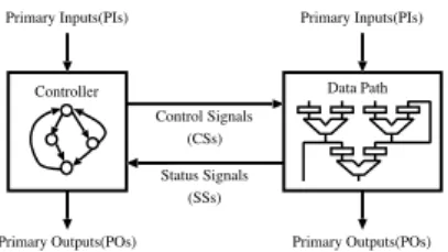
In RTL description, a VLSI circuit generally consists of a controller and a data path as shown in Figure 1. The for- mer is represented by an STG and the latter is represented by hardware elements (e.g. registers, multiplexers and operational modules) and signal lines connecting them. Each of the con- troller and the data path has primary inputs from the outside of the VLSI and primary outputs to the outside of the VLSI. The controller also has status inputs from the data path and control outputsto the data path. Similarly, the data path also has control inputs from the controller and status outputs to the controller. The signals from the controller to the data path are called control signals, and the signals from the data path to the controller are called status signals.
A data path consists of hardware elements and signal lines. Hardware elements are primary inputs, primary outputs, con-
1
Asia and South Pacific Design Automation Conference 2001(ASP-DAC2001), pp. 331-334, Feb. 2001.
Controller Data Path Control Signals
(CSs)
Status Signals (SSs)
Primary Inputs(PIs)
Primary Outputs(POs) Primary Inputs(PIs)
Primary Outputs(POs)
Fig. 1.An RTL controller/data path circuit.
trol inputs, status outputs, registers, multiplexors, and opera- tional modules. A signal line connects two hardware elements with some bit width. Inputs of a hardware element in the data path can be classified into data inputs and control inputs. Ex- amples of the control inputs are load enable signals of registers, selection signals of multiplexers and function selection signals of operational modules. Similarly, outputs of a hardware ele- ment of a data path can be classified into data outputs and sta- tus outputs. Comparators are examples of hardware elements having status outputs.
The following restrictions are introduced into our data path architecture in order to simplify the discussion, though they can be relaxed.
A1: All signal lines in the data path have the same bit width. A2: An operational module has only one or two data inputs
and only one data output.
A3: For any data input, there exists a path from a primary in- put. And for any data output, there exists a path to a primary output.
A4: Control inputs of a hardware element are connected di- rectly to control inputs of the data path. And status outputs of a hardware element are connected directly to status out- puts of the data path.
III. FIXED-CONTROLTESTABILITY
In this section, we define a new property of circuit struc- ture of data path called fixed-control testability which is a sub- class of strong testability. Strong testability is proposed as a characteristic of data paths that guarantees applicability of hi- erarchical test generation[6]. Hierarchical test generation is a promising way for testing very large sequential circuits. In the hierarchical test generation, testing for each hardware element Mproceeds as follows.
Step 1: Test patterns are generated for M (a combinational cir- cuit) using a combinational ATPG tool.
Step 2: The test patterns are applied to M: the values are fed through primary inputs at appropriate times, so that the de- sired test patterns can be applied to M.
Step 3: The responses of M to the test patterns are propagated to primary outputs for observation.
A test plan specifies the control signals so that the test pat- terns and the responses can be propagated. Strong testability of a data path is defined as follows.
Definition 1: Strong Testability [5]
A data path is strongly testable if there exists a test plan for each combinational hardware element M that makes it possible to apply any pattern to M and to observe any response of M. ✷ A strongly testable data path has the following advantages.
• Test pattern generation time is short since a combinational ATPG tool can be used for each combinational hardware el- ement separately.
• Test plan generation time is short since test plans are gener- ated at RTL (not at gate level).
• 100% fault efficiency can be achieved for the whole data
path, since each hardware element M under consideration is a combinational circuit of small size and strong testability guarantees complete controllability and observability of M in the data path.
Let T P be a test plan of a combinational hardware element Min a strongly testable data path. The test plan T P can propa- gate any pattern of M along several paths CP from primary in- puts to M. Similarly, T P propagates any response of M along several paths OP from M to primary outputs. The test plan T P generally consists of three phases: a control phase, a test phase and a observation phase. Here, let R(CP) be a set of registers which are the nearest registers from M on paths in CP and let R(OP) be a set of registers which are the nearest registers from Mon paths in OP.
Control phase: The sequence of control vectors corresponding to the control phase in T P propagates any pattern from pri- mary inputs of the data path to every register in R(CP) if R(CP) ̸= φ. Otherwise, the control phase is not necessary. Test phase: The control vector corresponding to the test phase
in T P propagates any pattern from primary inputs and/or every register in R(CP) and any response from data outputs of M to every register in R(OP) and/or primary outputs. Observation phase: The sequence of control vectors corre-
sponding to the observation phase in T P propagates re- sponses from every register in R(OP) to primary outputs if R(OP) ̸= φ. Otherwise, the observation phase is not neces- sary.
For a controller/data path circuit, test plans of the data path must be applied to control signals. In the test architecture of [3], we generate the test plans from inside of the circuit by ap- pending extra logic called a test plan generator (TP G) which generate test plans. For a strongly testable data path, a test plan for a hardware element of the data path can not be gen- erally composed of fixed control vectors such that control vec- tors of the test plan varies clock by clock. Therefore aTP G must be designed as a sequential circuit. If control vectors of a test plan do not vary, theTP G becomes combinational circuit and hence area overhead can be reduced. We introduce such a testability defined as follows.
Definition 2: Fixed-Control Testability
A data path is fixed-control testable if the following conditions hold.
C1: The data path is strongly testable.
C2: For each combinational hardware element M in the data path, a control sequence of each phase in a test plan of M is composed of only one control vector. ✷ In addition to advantages of strongly testable data paths, a fixed-control testable data path has the following advantage.
• A test plan of a combinational hardware element is com- posed of at most three control vectors.
IV. DFT METHOD FORDATAPATHS
In our DFT method for a data path, as many test patterns and responses of each hardware element as possible are propagated along existing data path flows in the data path. If test patterns and responses cannot be propagated along existing data path flows, the DFT method appends DFT elements (e.g. masks, multiplexersand bypass registers) to the data path to guarantee that the test patterns and the responses can be propagated along existing data path flows. We provide a brief explanation of the DFT method.
Consider testing of a combinational hardware element M with two data inputs, x and y, in the data path. To test M, a
2
value specified by a test pattern should be fed into x. We prop- agate the value along a path p from a primary input to x. If an operational module M′appears on p, the output value of M′ will depend on the function and the input value(s) of M′.
In order to guarantee that the data output of M′is completely controllable by the data input on p, thru function between the input and the output is added to M′. Most of the popular op- erational modules (e.g. adder) can realize the thru function by using a mask element. The mask element generates a constant which is required to realize the thru function. If we cannot re- alize the thru function using the mask element, we realize the thru function using a multiplexer. In the rest of this paper, we assume that, for every operational module, thru function can be realized by mask element in order to simplify the discussion.
However, we cannot achieve the fixed-control testability by adding only the thru functions. The thru functions guarantee controllability of a single path. To test M, a test pattern must be applied to both the inputs x and y simultaneously. Pres- ence of re-convergent paths in the data path can prevent such application of the test pattern to M. In particular, this can hap- pen if the propagation paths to the two inputs of M start from the same primary input and have the same sequential depth2. Such re-convergent paths will cause a timing conflict, i.e. two different values are required on a primary input at the same time. In the concept of strong testability [5], such conflicts are resolved by using hold functions of registers where a regis- ter originally has a hold function or is augmented with a hold function. However, since use of hold functions of registers spoils fixed-control testability, we cannot use the hold func- tions. To resolve such conflicts, in this DFT method, some registers are bypassed by multiplexers and bypass registers are added to some signal lines.
The goal of the DFT method is to make a given data path fixed-control testable with the minimum hardware overhead. Practical implementation of an algorithm for the DFT method also dictates that the computation time for the DFT insertion and test plan generation algorithms be manageable. We pro- pose a heuristic algorithm for the DFT method. The heuristic algorithm for the DFT proceeds in the following two stages. Stage 1 (Construct paths): For each data input of hardware el-
ements, we determine a path which is used to propagate test vectors from a primary input to the data input . Similarly, for each hardware element, we determine a path which is used to propagate responses from the data output to a primary out- put. In this stage, we pay attention to reduce test application time and minimizing the number of DFT elements added at the next stage.
Stage 2 (Add DFT elements): To ensure the propagation capa- bility of the paths determined at the Stage 1, we add DFT elements (thru function, multiplexer and bypass register) to the data path at strategic locations.
The limitation of space prevents us describing the details of the DFT algorithm. See [7].
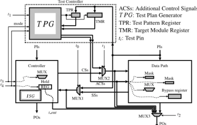
V. TESTARCHITECTURE OFRTL CIRCUITS
In our DFT for an RTL controller/data path circuit, we first apply the DFT method of [4] to the controller and apply the DFT method proposed in Section IV to the data path. Then, we embed mechanisms to enhance controllability and observ- ability of the control signals and the status signals in the same
2The number of registers on a path is called sequential depth of the path.
TP G: Test Plan Generator ACSs: Additional Control Signals
PIs
POs
PIs
POs TMR
TPR Test Controller
Controller
I SG MUX
Data Path
Mask
TP G
ACSs CSs
SSs
t0 t1
t2 t3t4
Mask
Bypass register Hold
REG
MUX1 MUX2
MUX3 t out
TPR: Test Pattern Register TMR: Target Module Register ti: Test Pin
t1 mode
MUX
Fig. 2.Test architecture of a controller/data path circuit.
way as the method of [3] so that the testing methods of con- trollers and data paths can be applied.
The test architecture of the controller/data path circuit of our method is shown in Figure 2. The circuit is configured by con- trolling test pins as shown in Table I.
TABLE I CONFIGURATIONS OF TEST
ARCHITECTURE. Test Pins
t0 t1 t2 t3 t4
Operation
0 0 0 0 0 Normal operation 1 0 1 ∗ ∗ Testing controller 0 1 ∗ ∗ ∗ Testing data path
∗: depend on test patterns or test plans
Since the test architecture of the circuit except for the test controllershown in Figure 2 is the same as that proposed in [3], we discuss only the test controller.
Test plans are generated for all the combinational hard-
ware elements in a data path of a circuit. In our test archi- tecture shown in Figure 2, all the test plans of the data path are generated by a test controller. The test controller consists of a test plan generator(TP G), a test pattern register(TPR) and a target module register(TMR).
TABLE II CONFIGURATION OF TEST
CONTROLLER. Mode
t3 t4
Function
0 0 Setting TPR and TMR 0 1 Control phase 1 0 Test phase 1 1 Observation phase
Let us consider the testing of a combinational hardware element M, which has data inputs and con- trol inputs, in the data path. The TMR is used to store the index of a test plan of M. The bit width of the TMR is log2m where m is the number of test plans for all the
combinational hardware elements in the data path. TheTP G generates a test plan if the index of the test plan is stored in the TMR. TheTP G is designed as a combinational circuit and controlled by t3 and t4 as shown in Table II. TheTP Ggener- ates a control vector for a phase of the test plan. A test pattern for the control inputs of M is pre-stored in the TPR before en- tering the control phase and is applied to the control inputs by way ofTP Gin the test phase. The load enable signal for TPR and TMR is controlled from the t3 and t4 by way ofTP G as shown in Table II. The mode switching signal t1is used to disable DFT elements of the data path in the normal operation mode of the circuit.
We also consider testing of aTP G. Since theTP G is not used at the normal operation, we test theTP Gonly to confirm that the test plans are generated correctly. It is performed by observing primary outputs of a data path by way of MUX3 (see Figure 2).
VI. EXPERIMENTALRESULTS
In this section, we evaluate effectiveness of our proposed method by experiments. Circuit characteristics of RTL bench-
3
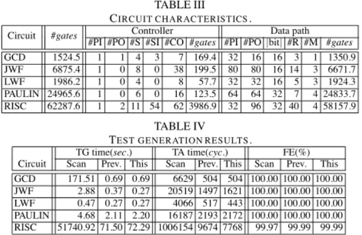
TABLE III CIRCUIT CHARACTERISTICS.
Controller Data path
Circuit #gates
#PI #PO #S #SI #CO #gates #PI #PO|bit| #R #M #gates
GCD 1524.5 1 1 4 3 7 169.4 32 16 16 3 1 1350.9
JWF 6875.4 1 0 8 0 38 199.5 80 80 16 14 3 6671.7
LWF 1986.2 1 0 4 0 8 57.7 32 32 16 5 3 1924.3
PAULIN 24965.6 1 0 6 0 16 123.5 64 64 32 7 4 24833.7 RISC 62287.6 1 2 11 54 62 3986.9 32 96 32 40 4 58157.9
TABLE IV TEST GENERATION RESULTS.
TG time(sec.) TA time(cyc.) FE(%) Circuit Scan Prev. This Scan Prev. This Scan Prev. This GCD 171.51 0.69 0.69 6629 504 504 100.00 100.00 100.00 JWF 2.88 0.37 0.27 20519 1497 1621 100.00 100.00 100.00 LWF 0.47 0.27 0.27 4066 517 443 100.00 100.00 100.00 PAULIN 4.68 2.11 2.20 16187 2193 2172 100.00 100.00 100.00 RISC 51740.92 71.50 72.29 1006154 9674 7768 99.97 99.99 99.99
mark circuits used in the experiments is shown in Table III. The circuits GCD, JWF, LWF and PAULIN are popularly used examples and the circuit RISC is a practical and large design. In our experiments, we used a logic synthesis tool AutoLogicII (Mentor Graphics) with its sample libraries to synthesize these benchmark circuits. In this table, column “#gates” denotes the total areas after synthesis. Here, areas are estimated using gate equivalent of the library cell area. Columns “#PI”, “#PO” and
“#gates” of columns “Controller” and “Data path” denote the numbers of primary inputs and primary outputs and circuit area of respective parts. Columns “#S”, “#SI” and “#CO” in “Con- troller” denote the numbers of states, of status inputs and of control outputs. Columns “|bit|”, “#R” and “#M” in “Data path” denote the bit width of data paths and the numbers of registers and of operational modules in data paths.
Test generation results are shown in Table IV. The ATPG tool TestGen (Synopsys) is used as a combinational ATPG tool in this experiments on Ultra60 model 2360 (Sun Microsys- tems). Columns “TG time”, “TA time” and “FE” denote test generation time in second, test application time in clock cy- cles and fault efficiency. In each of these columns, columns
“Scan”, “Prev.” and “This” denote the results of the circuits modified by the full-scan design, of the circuits modified by the method of our previous work[3] and of the circuits mod- ified by our proposed method in this work. Test generation time of the proposed method is almost the same as the method of [3]. Test generation time of the proposed method is shorter than that of the full-scan. Especially, for the circuit RISC, the proposed method can reduce to 1/700 of the full-scan design and can enhance fault efficiency compared to that of the full- scan design. For the circuit, fault efficiency is 99.99% because the combinational ATPG tool can not generate a test pattern for a fault in a multiplier of the circuit in the method of [3] and the proposed method. Test application time of the proposed method is shorter than the method of [3]. Test application time of the proposed method is drastically reduced compared with that of the full-scan design.
The area and pin overheads of the full-scan design, the method of [3] and the proposed method are shown in Table V. Columns “C”, “DP”, “TC” and “MUX” in columns “Prev.” and “This” of column “Area overhead” denote the area over- head of controllers, data paths, test controllers and multiplex- ers added to control signals, status signals and primary outputs of data paths. In the proposed method, area overhead of test controller is less compared to the method of [3]. Furthermore, for data paths, however a fixed-control testable data path can achieve simpler test plans compared to strong testable one, the difference between the area overhead of the proposed method
TABLE V HARDWARE OVERHEADS.
Area overhead(%) Pin overhead(#)
Circuit Scan Prev. This
C DP TC MUX C DP TC MUXScan Prev. This GCD 26.6 39.7 1.1 2.6 23.2 12.8 32.8 1.1 2.6 16.3 12.8 3 5 5 JWF 26.7 37.1 0.4 5.2 21.9 9.7 41.9 0.4 9.3 22.1 10.0 3 5 5 LWF 33.4 48.6 0.8 18.1 21.1 8.6 44.6 0.8 18.1 17.1 8.6 3 5 5 PAULIN 7.4 8.1 0.2 1.2 5.3 1.4 7.1 0.2 2.5 3.0 1.4 3 5 5 RISC 16.7 27.3 0.1 10.9 12.5 3.6 21.0 0.1 9.6 7.6 3.7 3 6 6
and that of the method of [3] is not large. Especially, for RISC, the proposed method can reduce the area overhead compared with the method of [3]. In these results, area overhead of the proposed method is less than that of the method of [3] for all circuits except JWF. The area overhead of the proposed method is larger than that of the full-scan design but the difference be- tween the area overhead of the proposed method and that of the full-scan design is not large. The pin overhead of the proposed method is the same as the method of [3] and larger than that of the full-scan design. In return for these disadvantages, the proposed method allows at-speed testing.
VII. CONCLUSION
This paper presented a non-scan DFT method for con- troller/data path circuits designed at RTL and that for data path based on fixed-control testability. The proposed method can achieve 100% fault efficiency and allows at-speed testing. We reduced the hardware overhead in the presented method com- pared to the method of our previous work [3]. The hardware overhead of the method is slightly more than that of the full- scan design. Since the hierarchical test generation can be ap- plied to the data path part of the circuits, test generation time of the proposed method is shorter than that of the full-scan design. Furthermore, since the proposed method uses no tradi- tional scan path, test application time is very low.
Acknowledgments This work was supported in part by Semi- conductor Technology Academic Research Center (STARC) under the Research Project.
REFERENCES
[1] H. Fujiwara: Logic Testing and Design for Testability, The MIT Press, 1985.
[2] P. C. Maxwell, R. C. Aitken, V. Johansen and I. Chiang: “The effect of different test sets on quality level prediction: when is 80% better than 90%?,” in Proc. of Int. Test Conf., pp. 358–364, 1991.
[3] S. Ohtake, H. Wada, T. Masuzawa and H. Fujiwara: “A non-scan DFT method at register-transfer level to achieve complete fault efficiency,” in Proc. of Asian South Pacific Design Automation Conference (ASP-DAC), pp. 599–604, 2000.
[4] S. Ohtake, T. Masuzawa and H. Fujiwara: “A non-scan DFT method for controllers to achieve complete fault efficiency,” in Proc. of the 7th Asian test symposium, pp. 204–211, 1998.
[5] H. Wada, T. Masuzawa, K. K. Saluja and H. Fujiwara: “Design for strong testability of RTL data paths to provide complete fault efficiency,” in Proc. of Int. Conf. on VLSI Design, pp. 300–305, 2000.
[6] B. T. Murray and J. P. Hayes: “Hierarchical test generation using pre com- puted tests for modules,” IEEE Trans. on CAD, Vol. 9, No. 6, pp. 594–603, June 1990.
[7] S. Ohtake, S. Nagai, H. Wada, and H. Fujiwara: “A non-scan DFT method at RTL based on fixed-control testability to achieve 100% fault efficiency,” Technical report, Information Science Technical Report: TR2000009 (http://isw3.aist-nara.ac.jp/IS/TechReport2/report/2000009.ps), Nara In- stitute of Science and Technology, 2000.
4