PIC18(L)F2X/45K50
Universal Serial Bus Features:
• USB V2.0 Compliant
• Crystal-less Full Speed (12 Mb/s) and Low-Speed Operation (1.5 Mb/s)
• Supports Control, Interrupt, Isochronous and Bulk Transfers
• Supports up to 32 Endpoints (16 Bidirectional)
• 1 Kbyte Dual Access RAM for USB
• On-Chip USB Transceiver
Flexible Oscillator Structure:
• 3x and 4xPLL Clock Multipliers
• Two External Clock modes, Up to 48 MHz (12 MIPS)
• Internal 31 kHz Oscillator
• Internal Oscillator, 31 kHz to 16 MHz - Factory calibrated to ± 1%
- Self-tune to ± 0.20% max. from USB or secondary oscillator
• Secondary Oscillator using Timer1 @ 32 kHz
• Fail-Safe Clock Monitor:
- Allows for safe shutdown if any clock stops
Peripheral Highlights:
• Up to 33 I/O pins plus 3 Input-Only Pins: - High-current Sink/Source 25 mA/25 mA - Three programmable external interrupts - 11 programmable interrupts-on-change - Nine programmable weak pull-ups - Programmable slew rate
• SR Latch
• Enhanced Capture/Compare/PWM (ECCP) module:
- One, two or four PWM outputs - Selectable polarity
- Programmable dead time - Auto-shutdown and auto-restart - Pulse steering control
• Capture/Compare/PWM (CCP) module
• Master Synchronous Serial Port (MSSP) module Supporting 3-Wire SPI (all four modes) and I2C™ Master and Slave modes
• Two Analog Comparators with Input Multiplexing
• 10-Bit Analog-to-Digital (A/D) Converter module: - Up to 25 input channels
- Auto-acquisition capability - Conversion available during Sleep
• Digital-to-Analog Converter (DAC) module: - Fixed Voltage Reference (FVR) with 1.024V,
2.048V and 4.096V output levels
- 5-bit rail-to-rail resistive DAC with positive and negative reference selection
• High/Low-Voltage Detect module
• Charge Time Measurement Unit (CTMU): - Supports capacitive touch sensing for touch
screens and capacitive switches
• Enhanced USART module:
- Supports RS-485, RS-232 and LIN/J2602 - Auto-wake-up on Start bit
- Auto-Baud Detect
Extreme Low-Power Management with
XLP:
• Sleep mode: 20 nA, typical
• Watchdog Timer: 300 nA, typical
• Timer1 Oscillator: 800 nA @ 32 kHz
• Peripheral Module Disable
Special Microcontroller Features:
• Low-Power, High-Speed CMOS Flash Technology
• C Compiler Optimized Architecture for Re-Entrant Code
• Power Management Features:
- Run: CPU on, peripherals on, SRAM on - Idle: CPU off, peripherals on, SRAM on - Sleep: CPU off, peripherals off, SRAM on
• Priority Levels for Interrupts
• Self-Programmable under Software Control
• 8 x 8 Single-Cycle Hardware Multiplier
• Extended Watchdog Timer (WDT): - Programmable period from 4 ms to 131s
• Single-Supply In-Circuit Serial Programming™ (ICSP™) via Two Pins
• In-Circuit Debug (ICD) with Three Breakpoints via Two Pins
• Optional dedicated ICD/ICSP Port (44-pin TQFP Package Only)
• Wide Operating Voltage Range: - F devices: 2.3V to 5.5V - LF devices: 1.8V to 3.6V
• Flash Program Memory of 10,000 Erase/Write Cycles Minimum and 20-year Data Retention
28/40/44-Pin, Low-Power, High-Performance
Microcontrollers with XLP Technology
PIC18(L)F2X/45K50
PIC18(L)F2X/45K50 Family Types
Pin Diagrams
FIGURE 1: 28-PIN SPDIP (300 MIL), SOIC, SSOP
FIGURE 2: 28-PIN QFN
Device
Program Memory Data Memory
Pins I/O
10-Bit A/D Channels Comparators CCP/ ECCP BOR/LVD CTMU MSSP EUSART Timers 8-bit/16-bit USB 2.0
Flash (bytes)
Single-Word Instructions
SRAM (bytes)
Data EEPROM
(bytes)
PIC18(L)F45K50 32K 16384 2048 256 40/44 36 25-ch 2 1/1 Yes Yes 1 1 2/2 Yes
PIC18(L)F25K50 32K 16384 2048 256 28 25 14-ch 2 1/1 Yes Yes 1 1 2/2 Yes
PIC18(L)F24K50 16K 8192 2048 256 28 25 14-ch 2 1/1 Yes Yes 1 1 2/2 Yes
10 11 2 3 4 5 6 1
8 7
9
12 13
14 15
16 17 18 19 20 23 24 25 26 27 28
22 21 MCLR/VPP/RE3
RA0 RA1 RA2 RA3 RA4 RA5 VSS RA7 RA6 RC0 RC1 RC2 VUSB3V3
RB7 RB6 RB5 RB4 RB3 RB2 RB1 RB0 VDD VSS RC7 RC6 D+ D-
PIC18(L)F2XK50
10 11
2 3
6 1
18 19 20 21
27 12 13 14 15
8
7
16 17
26 25 24 23 22
28 9RC0
5 4
RB7 RB6 RB5 RB4
RB3 RB2 RB1 RB0 VDD VSS RC7
RC6D+D-
MCLR/VPP/RE3RA0RA1
RA2 RA3 RA4 RA5 VSS RA7 RA6
RC1 RC2 VUSB3V3
PIC18(L)F2XK50
Note: For the QFN package, it is recommended that the bottom pad be connected to VSS.
PIC18(L)F2X/45K50
FIGURE 3: 40-PIN PDIP (600 MIL)
FIGURE 4: 40-PIN UQFN
RB7 RB6 RB5 RB4 RB3 RB2 RB1 RB0 VDD VSS RD7 RD6 RD5 RD4 RC7 RC6 D+ D- RD3 RD2 MCLR/VPP/RE3
RA0 RA1 RA2 RA3 RA4 RA5 RE0 RE1 RE2 VDD VSS RA7 RA6 RC0 RC1 RC2 VUSB3V3 RD0 RD1
1 2 3 4 5 6 7 8 9 10 11 12 13 14 15 16 17 18 19 20
40 39 38 37 36 35 34 33 32 31 30 29 28 27 26 25 24 23 22 21
PIC18(L)F45K50
10 2 3 4 5 6 1
17 18 19 20
11 12 13 14 34
8 7
40 39 38 37 36 3515 16
27 28 29 30
21 22 23 24 25 26
32 31
9
33 RA3RA2RA1RA0MCLR/VPP/RE3
RB3 RB7RB6RB5RB4RC6 D+ D- RD3 RD2 RD1 RD0 VUSB3V3 RC2 RC1
RA6 RA7 VSS VDD RE2 RE1 RE0 RA5 RA4 RC7
RD4 RD5 RD6 RD7 VSS VDD RB0 RB1 RB2
PIC18(L)F45K50
RC0
Note: For the UQFN package, it is recommended that the bottom pad be connected to VSS.
PIC18(L)F2X/45K50
FIGURE 5: 44-PIN TQFP
10 11 2 3
6 1
18 19 20 21 22
12 13 14 15 38
8 7
44 43 42 41 40 3916 17
29 30 31 32 33
23 24 25 26 27 28
36 3435
9
37 RA3RA2RA1RA0MCLR/VPP/RE3
NC/ICCK(1)/ICPGC(1) RB7RB6RB5RB4NC/ICDT(1)/ICPGD(1)RC6 D+ D- RD3 RD2 RD1 RD0 VUSB3V3 RC2 NC
NC/ICRST(1)/ICVPP(1) RC0
RA6 RA7 VSS VDD RE2 RE1 RE0 RA5 RA4 RC7
RD4 RD5 RD6 VSS VDD RB0 RB1 RB2 RB3
RD7 5
4
RC1
PIC18(L)F45K50
Note 1: Special ICPORT programming/debug port features available when ICPRT =1
2012-2014 Microchip Technology Inc.DS30000684B-page 5
PIC18(L)F2X/45K50
TABLE 1: PIC18(L)F2X/45K50 PIN SUMMARY
I/O 28-Pin SPDIP/SOIC/SSOP 28-Pin QFN 40-Pin PDIP 40-Pin UQFN 44-Pin TQFP Analog Comparator CTMU SR Latch Reference USB (E)CCP EUSART MSSP Timers Interrupts Pull-up Basic ICD
RA0 2 27 2 17 19 AN0 C12IN0- — — — — — — — — — — — —
RA1 3 28 3 18 20 AN1 C12IN1- CTCMP — — — — — — — — — — —
RA2 4 1 4 19 21 AN2 C2IN+ — — VREF-
DACOUT
— — — — — — — — —
RA3 5 2 5 20 22 AN3 C1IN+ — — VREF+ — — — — — — — — —
RA4 6 3 6 21 23 — C1OUT — SRQ — — — — — T0CKI — — — —
RA5 7 4 7 22 24 AN4 C2OUT SRNQ HLVDIN — — — SS — — — — —
RA6 10 7 14 29 31 — — — — — — — — — — — — OSC2
CLKO
—
RA7 9 6 13 28 30 — — — — — — — — — — — — OSC1
CLKI
—
RB0 21 18 33 8 8 AN12 — — SRI — — FLT0 — SDI
SDA
— INT0 Y — —
RB1 22 19 34 9 9 AN10 C12IN3- — — — — P1C(5) — SCK
SCL
— INT1 Y — —
RB2 23 20 35 10 10 AN8 — CTED1 — — — P1B(5) — — — INT2 Y — —
RB3 24 21 36 11 11 AN9 C12IN2- CTED2 — — — CCP2(1) — SDO — — — — —
RB4 25 22 37 12 14 AN11 — — — — — P1D(5) — — — IOCB4 Y — —
RB5 26 23 38 13 15 AN13 — — — — — — — — T1G
T3CKI(2)
IOCB5 — — —
RB6 27 24 39 14 16 — — — — — — — — — — IOCB6 Y PGC —
Note 1: Alternate CCP2 pin location based on Configuration bit. 2: Alternate T3CKI pin location based on Configuration bits. 3: Pins are enabled when ICPRT =1, otherwise, they are disabled.
4: Location on 40/44-Pin parts (PIC18(L)F45K50). Function not on this pin on 28-Pin parts (PIC18(L)F2XK50). 5: Location on 28-Pin parts (PIC18(L)F2XK50). Function not on this pin on 40/44-Pin parts (PIC18(L)F45K50). 6: Alternate SDO pin location based on Configuration bits.
7: RE3 can be used for digital input only (no output functionality).
PIC18(L)F2X/45K50
DS30000684B-page 6 2012-2014 Microchip Technology In
RB7 28 25 40 15 17 — — — — — — — — — — IOCB7 Y PGD —
RC0 11 8 15 30 32 — — — — — — — — — SOSCO
T1CKI T3CKI T3G
IOCC0 — — —
RC1 12 9 16 31 35 — — — — — — CCP2 — — SOSCI IOCC1 — — —
RC2 13 10 17 32 36 AN14 — CTPLS — — — CCP1
P1A
— — — IOCC2 — — —
— 14 11 18 33 37 — — — — — VUSB3V3 — — — — — — VDDCORE —
— 15 12 23 38 42 — — — — — D- — — — — IOCC4 — — —
— 16 13 24 39 43 — — — — — D+ — — — — IOCC5 — — —
RC6 17 14 25 40 44 AN18 — — — — — — TX
CK
— — IOCC6 — — —
RC7 18 15 26 1 1 AN19 — — — — — — RX
DT
SDO(6) — IOCC7 — — —
RD0 — — 19 34 38 AN20 — — — — — — — — — — — — —
RD1 — — 20 35 39 AN21 — — — — — — — — — — — — —
RD2 — — 21 36 40 AN22 — — — — — — — — — — — — —
RD3 — — 22 37 41 AN23 — — — — — — — — — — — — —
RD4 — — 27 2 2 AN24 — — — — — — — — — — — — —
RD5 — — 28 3 3 AN25 — — — — — P1B(4) — — — — — — —
RD6 — — 29 4 4 AN26 — — — — — P1C(4) — — — — — — —
RD7 — — 30 5 5 AN27 — — — — — P1D(4) — — — — — — —
TABLE 1: PIC18(L)F2X/45K50 PIN SUMMARY (CONTINUED)
I/O 28-Pin SPDIP/SOIC/SSOP 28-Pin QFN 40-Pin PDIP 40-Pin UQFN 44-Pin TQFP Analog Comparator CTMU SR Latch Reference USB (E)CCP EUSART MSSP Timers Interrupts Pull-up Basic ICD
Note 1: Alternate CCP2 pin location based on Configuration bit. 2: Alternate T3CKI pin location based on Configuration bits. 3: Pins are enabled when ICPRT =1, otherwise, they are disabled.
4: Location on 40/44-Pin parts (PIC18(L)F45K50). Function not on this pin on 28-Pin parts (PIC18(L)F2XK50). 5: Location on 28-Pin parts (PIC18(L)F2XK50). Function not on this pin on 40/44-Pin parts (PIC18(L)F45K50). 6: Alternate SDO pin location based on Configuration bits.
2012-2014 Microchip Technology Inc.DS30000684B-page 7
PIC18(L)F2X/45K50
RE0 — — 8 23 25 AN5 — — — — — — — — — — — — —
RE1 — — 9 24 26 AN6 — — — — — — — — — — — — —
RE2 — — 10 25 27 AN7 — — — — — — — — — — — — —
RE3(7) 1 26 1 16 18 — — — — — — — — — — — Y MCLR
VPP
—
— 20 17 11,
32 7, 26
7, 28
— — — — — — — — — — — — VDD —
— 8,
19 5, 16
12, 31
6, 27
6, 29
— — — — — — — — — — — — VSS —
— — — – –- 12(3) — — — — — — — — — — — — ICPGC(3) ICCK(3)
— — — – –- 13(3) — — — — — — — — — — — — ICPGD(3) ICDT(3)
— — — –- –- 33(3) — — — — — — — — — — — — ICVPP(3) ICRST(3)
TABLE 1: PIC18(L)F2X/45K50 PIN SUMMARY (CONTINUED)
I/O 28-Pin SPDIP/SOIC/SSOP 28-Pin QFN 40-Pin PDIP 40-Pin UQFN 44-Pin TQFP Analog Comparator CTMU SR Latch Reference USB (E)CCP EUSART MSSP Timers Interrupts Pull-up Basic ICD
Note 1: Alternate CCP2 pin location based on Configuration bit. 2: Alternate T3CKI pin location based on Configuration bits. 3: Pins are enabled when ICPRT =1, otherwise, they are disabled.
4: Location on 40/44-Pin parts (PIC18(L)F45K50). Function not on this pin on 28-Pin parts (PIC18(L)F2XK50). 5: Location on 28-Pin parts (PIC18(L)F2XK50). Function not on this pin on 40/44-Pin parts (PIC18(L)F45K50). 6: Alternate SDO pin location based on Configuration bits.
7: RE3 can be used for digital input only (no output functionality).
PIC18(L)F2X/45K50
Table of Contents
1.0 Device Overview ... 10
2.0 Guidelines for Getting Started with PIC18(L)F2X/45K50 Microcontrollers ... 23
3.0 Oscillator Module (With Fail-Safe Clock Monitor)... 28
4.0 Power-Managed Modes ... 52
5.0 Reset ... 63
6.0 Memory Organization ... 73
7.0 Flash Program Memory ... 95
8.0 Data EEPROM Memory ... 104
9.0 8 x 8 Hardware Multiplier... 109
10.0 Interrupts ... 111
11.0 I/O Ports ... 128
12.0 Timer0 Module... 153
13.0 Timer1/3 Module with Gate Control... 156
14.0 Timer2 Module... 168
15.0 Capture/Compare/PWM Modules... 172
16.0 Master Synchronous Serial Port (MSSP) Module ... 203
17.0 Enhanced Universal Synchronous Asynchronous Receiver Transmitter (EUSART) ... 258
18.0 Analog-to-Digital Converter (ADC) Module ... 287
19.0 Comparator Module... 301
20.0 Charge Time Measurement Unit (CTMU)... 310
21.0 SR Latch... 325
22.0 Fixed Voltage Reference (FVR)... 330
23.0 Digital-to-Analog Converter (DAC) Module ... 332
24.0 Universal Serial Bus (USB) ... 336
25.0 High/Low-Voltage Detect (HLVD) ... 364
26.0 Special Features of the CPU ... 370
27.0 Instruction Set Summary ... 390
28.0 Development Support... 440
29.0 Electrical Specifications ... 444
30.0 DC and AC Characteristics Graphs and Charts ... 485
31.0 Packaging Information... 486
Appendix A: Revision History... 503
Appendix B: Device Differences... 504
The Microchip Web Site ... 505
Customer Change Notification Service ... 505
Customer Support ... 505
Product Identification System... 506
PIC18(L)F2X/45K50
TO OUR VALUED CUSTOMERS
It is our intention to provide our valued customers with the best documentation possible to ensure successful use of your Microchip products. To this end, we will continue to improve our publications to better suit your needs. Our publications will be refined and enhanced as new volumes and updates are introduced.
If you have any questions or comments regarding this publication, please contact the Marketing Communications Department via E-mail at [email protected]. We welcome your feedback.
Most Current Data Sheet
To obtain the most up-to-date version of this data sheet, please register at our Worldwide Web site at: http://www.microchip.com
You can determine the version of a data sheet by examining its literature number found on the bottom outside corner of any page. The last character of the literature number is the version number, (e.g., DS30000000A is version A of document DS30000000).
Errata
An errata sheet, describing minor operational differences from the data sheet and recommended workarounds, may exist for current devices. As device/documentation issues become known to us, we will publish an errata sheet. The errata will specify the revision of silicon and revision of document to which it applies.
To determine if an errata sheet exists for a particular device, please check with one of the following:
• Microchip’s Worldwide Web site; http://www.microchip.com
• Your local Microchip sales office (see last page)
When contacting a sales office, please specify which device, revision of silicon and data sheet (include literature number) you are using.
Customer Notification System
Register on our web site at www.microchip.com to receive the most current information on all of our products.
PIC18(L)F2X/45K50
1.0 DEVICE OVERVIEW
This document contains device-specific information for the following devices:
This family offers the advantages of all PIC18 microcontrollers – namely, high computational performance at an economical price – with the addition of high-endurance, Flash program memory. On top of these features, the PIC18(L)F2X/45K50 family introduces design enhancements that make these microcontrollers a logical choice for many high-performance, power sensitive applications.
1.1 New Core Features
1.1.1 XLP TECHNOLOGY
All of the devices in the PIC18(L)F2X/45K50 family incorporate a range of features that can significantly reduce power consumption during operation. Key items include:
• Alternate Run Modes: By clocking the controller from the Timer1 source or the internal oscillator block, power consumption during code execution can be reduced by as much as 90%.
• Multiple Idle Modes: The controller can also run with its CPU core disabled but the peripherals still active. In these states, power consumption can be reduced even further, to as little as 4% of normal operation requirements.
• Peripheral Module Disable bits: User code can power down individual peripheral modules during Run and Idle modes for further lowering dynamic power reduction.
• On-the-fly Mode Switching: The power-
managed modes are invoked by user code during operation, allowing the user to incorporate power-saving ideas into their application’s software design.
• Low Consumption in Key Modules: The power requirements for both Timer1 and the Watchdog Timer are minimized. See Section 29.0 “Electri- cal Specifications” for values.
1.1.2 UNIVERSAL SERIAL BUS (USB) Devices in the PIC18(L)F2X/45K50 family incorporate a fully-featured USB communications module with a built-in transceiver that is compliant with the USB Specification Revision 2.0. The module supports both low-speed and full-speed communication for all supported data transfer types. The device
1.1.3 MULTIPLE OSCILLATOR OPTIONS AND FEATURES
All of the devices in the PIC18(L)F2X/45K50 family offer ten different oscillator options, allowing users a wide range of choices in developing application hardware. These include:
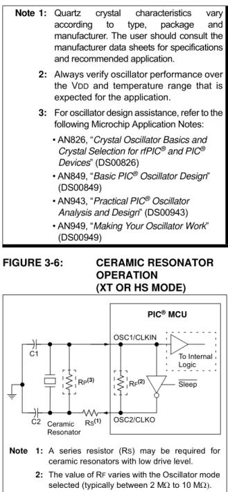
• Four Crystal modes, using crystals or ceramic resonators
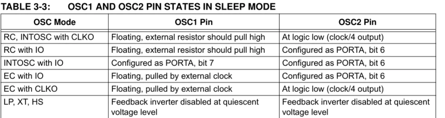
• Six External Clock modes, offering the option of using two pins (oscillator input and a divide-by- four clock output) or one pin (oscillator input, with the second pin reassigned as general I/O)
• Two External RC Oscillator modes with the same pin options as the External Clock modes
• An internal oscillator block which contains a 16 MHz HFINTOSC oscillator and a 31 kHz INTRC oscillator, which together provide eight user selectable clock frequencies, from 31 kHz to 16 MHz. This option frees the two oscillator pins for use as additional general purpose I/O.
• 3x and 4x Phase Lock Loop (PLL) frequency multipliers, available to both external and internal oscillator modes, which allows clock speeds of up to 48 MHz. Used with the internal oscillator, the PLL gives users a complete selection of clock speeds, from 31 kHz to 48 MHz – all without using an external crystal or clock circuit.
Besides its availability as a clock source, the internal oscillator block provides a stable reference source that gives the family additional features for robust operation:
• Active Clock Tuning: This option allows the internal oscillator to automatically tune itself to match USB host or external 32.768 kHz secondary oscillator clock sources. Full-speed USB operation can now meet specification requirements without an external crystal, enabling lower-cost designs.
• Fail-Safe Clock Monitor: This option constantly monitors the main clock source against a reference signal provided by the INTRC. If a clock failure occurs, the controller is switched to the internal oscillator block, allowing for continued operation or a safe application shutdown.
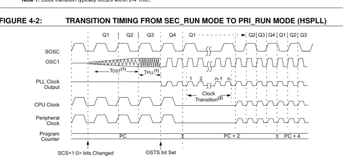
• Two-Speed Start-up: This option allows the internal oscillator to serve as the clock source from Power-on Reset, or wake-up from Sleep mode, until the primary clock source is available.
• PIC18(L)F45K50
• PIC18(L)F25K50
• PIC18(L)F24K50
PIC18(L)F2X/45K50
1.2 Other Special Features
• Memory Endurance: The Flash cells for both program memory and data EEPROM are rated to last for many thousands of erase/write cycles – up to 10K for program memory and 100K for EEPROM. Data retention without refresh is conservatively estimated to be greater than 40 years.
• Self-Programmability: These devices can write to their own program memory spaces under internal software control. By using a bootloader routine located in the protected Boot Block at the top of program memory, it becomes possible to create an application that can update itself in the field.
• Extended Instruction Set: The PIC18(L)F2X/ 45K50 family introduces an optional extension to the PIC18 instruction set, which adds eight new instructions and an Indexed Addressing mode. This extension, enabled as a device configuration option, has been specifically designed to optimize re-entrant application code originally developed in high-level languages, such as C.
• Enhanced CCP module: In PWM mode, this module provides 1, 2 or 4 modulated outputs for controlling half-bridge and full-bridge drivers. Other features include:
- Auto-shutdown, for disabling PWM outputs on interrupt or other select conditions - Auto-restart, to reactivate outputs once the
condition has cleared
- Output steering to selectively enable one or more of four outputs to provide the PWM signal.
• Enhanced Addressable EUSART: This serial communication module is capable of standard RS-232 operation and provides support for the LIN bus protocol. Other enhancements include automatic baud rate detection and a 16-bit Baud Rate Generator for improved resolution. When the microcontroller is using the internal oscillator block, the EUSART provides stable operation for applications that talk to the outside world without using an external crystal (or its accompanying power requirement).
• 10-Bit A/D Converter: This module incorporates programmable acquisition time, allowing for a channel to be selected and a conversion to be initiated without waiting for a sampling period and thus, reduce code overhead.
• Dedicated ICD/ICSP™ Port: These devices introduce the use of debugger and programming pins that are not multiplexed with other
microcontroller features. Offered as an option in the TQFP packaged devices, this feature allows users to develop I/O intensive applications while retaining the ability to program and debug in the circuit.
• Charge Time Measurement Unit (CTMU): The CTMU is a flexible analog module that provides accurate differential time measurement between pulse sources, as well as asynchronous pulse generation. Together with other on-chip analog modules, the CTMU can precisely measure time, measure capacitance or relative changes in capacitance or generate output pulses that are independent of the system clock.
• SR Latch Output: A single SR latch with multiple Set and Reset inputs as well as separate latch outputs.
1.3 Details on Individual Family
Members
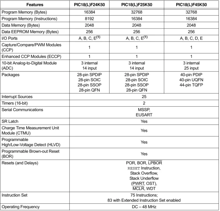
Devices in the PIC18(L)F2X/45K50 family are available in 28-pin and 40/44-pin packages. The block diagram for the device family is shown in Figure 1-1.
The devices have the following differences: 1. Flash program memory
2. A/D channels 3. I/O ports
4. Input Voltage Range/Power Consumption All other features for devices in this family are identical. These are summarized in Table 1-1.
The pinouts for all devices are listed in the pin summary table (Table 1) and I/O description tables (Table 1-2 and Table 1-3).
PIC18(L)F2X/45K50
TABLE 1-1: DEVICE FEATURES
Features PIC18(L)F24K50 PIC18(L)F25K50 PIC18(L)F45K50
Program Memory (Bytes) 16384 32768 32768
Program Memory (Instructions) 8192 16384 16384
Data Memory (Bytes) 2048 2048 2048
Data EEPROM Memory (Bytes) 256 256 256
I/O Ports A, B, C, E(1) A, B, C, E(1) A, B, C, D, E
Capture/Compare/PWM Modules
(CCP) 1 1 1
Enhanced CCP Modules (ECCP) 1 1 1
10-bit Analog-to-Digital Module (ADC)
3 internal 14 input
3 internal 14 input
3 internal 25 input
Packages 28-pin SPDIP
28-pin SOIC 28-pin SSOP
28-pin QFN
28-pin SPDIP 28-pin SOIC 28-pin SSOP
28-pin QFN
40-pin PDIP 40-pin UQFN 44-pin TQFP
Interrupt Sources 25
Timers (16-bit) 2
Serial Communications MSSP,
EUSART
SR Latch Yes
Charge Time Measurement Unit
Module (CTMU) Yes
Programmable
High/Low-Voltage Detect (HLVD) Yes
Programmable Brown-out Reset
(BOR) Yes
Resets (and Delays) POR, BOR, LPBOR
RESET Instruction, Stack Overflow, Stack Underflow
(PWRT, OST), MCLR, WDT
Instruction Set 75 Instructions;
83 with Extended Instruction Set enabled
Operating Frequency DC – 48 MHz
Note 1: PORTE contains the single RE3 read-only bit.
PIC18(L)F2X/45K50
FIGURE 1-1: PIC18(L)F2X/45K50 FAMILY BLOCK DIAGRAM
Instruction Decode and
Control
Data Latch Data Memory
Address Latch
Data Address<12> 12
Access BSR FSR0
FSR1 FSR2
inc/dec logic
Address
4 12 4
PCH PCL PCLATH
8
31-Level Stack Program Counter
PRODL PRODH
8 x 8 Multiply
8 BITOP
8 8
ALU<8> 20
8 8 Table Pointer<21>
inc/dec logic
21
8 Data Bus<8>
Table Latch 8
IR
12
3 ROM Latch
PCLATU
PCU
Note 1: RE3 is only available when MCLR functionality is disabled.
2: OSC1/CLKIN and OSC2/CLKO are only available in select oscillator modes and when these pins are not being used as digital I/O. Refer to Section 6.0 “Memory Organization” for additional information.
EUSART
Comparators MSSP
10-bit ADC Timer2
Timer1 CTMU
Timer0
USB HLVD
ECCP1
BOR Data
EEPROM
W Instruction Bus <16>
STKPTR Bank
8 State machine
control signals
Decode
8
Power-up 8 Timer Oscillator Start-up Timer
Power-on Reset Watchdog
Timer OSC1(2)
OSC2(2)
Brown-out Reset Internal
Oscillator
Fail-Safe Clock Monitor
Precision ReferenceBand Gap MCLR(1)
Block INTRC Oscillator
16 MHz Oscillator Single-Supply Programming In-Circuit Debugger SOSCO
SOSCI
FVR
FVR FVR DAC
Address Latch Program Memory
(16/32 Kbytes) Data Latch
PORTA RA0:RA7
PORTB RB0:RB7
PORTC RC0:RC3
PORTD RD0:RD7
Timer3
SR Latch
C1/C2 CCP2
PORTE RE0:RE2
RE3(1)
DAC RC6:RC7
DAC
PIC18(L)F2X/45K50
TABLE 1-2: PIC18(L)F2XK50 PINOUT I/O DESCRIPTIONS
Pin Number
Pin Name Pin
Type
Buffer
Type Description
SPDIP, SOIC, SSOP
QFN
2 27 RA0/C12IN0-/AN0
RA0 I/O TTL/DIG Digital I/O.
C12IN0- I Analog Comparators C1 and C2 inverting input.
AN0 I Analog Analog input 0.
3 28 RA1/C12IN1-/AN1
RA1 I/O TTL/DIG Digital I/O.
C12IN1- I Analog Comparators C1 and C2 inverting input.
AN1 I Analog Analog input 1.
4 1 RA2/C2IN+/AN2/DACOUT/VREF-
RA2 I/O TTL/DIG Digital I/O.
C2IN+ I Analog Comparator C2 non-inverting input.
AN2 I Analog Analog input 2.
DACOUT O Analog DAC Reference output.
VREF- I Analog A/D reference voltage (low) input. 5 2 RA3/C1IN+/AN3/VREF+
RA3 I/O TTL/DIG Digital I/O.
C1IN+ I Analog Comparator C1 non-inverting input.
AN3 I Analog Analog input 3.
VREF+ I Analog A/D reference voltage (high) input.
6 3 RA4/C1OUT/SRQ/T0CKI
RA4 I/O ST/DIG Digital I/O.
C1OUT O DIG Comparator C1 output.
SRQ O DIG SR latch Q output.
T0CKI I ST Timer0 external clock input.
7 4 RA5/C2OUT/SRNQ/SS/HLVDIN/AN4
RA5 I/O TTL/DIG Digital I/O.
C2OUT O DIG Comparator C2 output.
SRNQ O DIG SR latch Q output.
SS I TTL SPI slave select input (MSSP).
HLVDIN I Analog High/Low-Voltage Detect input.
AN4 I Analog Analog input 4.
10 7 RA6/CLKO/OSC2
RA6 I/O TTL/DIG Digital I/O.
CLKO O DIG Outputs 1/4 the frequency of OSC1 and denotes the instruction cycle rate.
OSC2 O — Oscillator crystal output. Connects to crystal or resonator in Crystal Oscillator modes.
Legend: TTL = TTL compatible input; CMOS = CMOS compatible input or output; ST = Schmitt Trigger input with CMOS levels; I = Input; O = Output; P = Power.
Note 1: Default pin assignment for SDO, T3CKI and CCP2 when Configuration bits SDOMX, T3CMX and CCP2MX are set. 2: Alternate pin assignment for SDO, T3CKI and CCP2 when Configuration bits SDOMX, T3CMX and CCP2MX are clear.
PIC18(L)F2X/45K50
9 6 RA7/CLKI/OSC1
RA7 I/O TTL/DIG Digital I/O.
CLKI I CMOS External clock source input. Always associated with pin function OSC1.
OSC1 I ST Oscillator crystal input or external clock source input ST buffer when configured in RC mode; CMOS otherwise.
21 18 RB0/INT0/FLT0/SRI/SDI/SDA/AN12
RB0 I/O TTL/DIG Digital Output or Input with internal pull-up option.
INT0 I ST External interrupt 0.
FLT0 I ST PWM Fault input for ECCP auto-shutdown.
SRI I ST SR latch input.
SDI I ST SPI data in (MSSP).
SDA I/O I2C™ I2C data I/O (MSSP).
AN12 I Analog Analog input 12.
22 19 RB1/INT1/P1C/SCK/SCL/C12IN3-/AN10
RB1 I/O TTL/DIG Digital Output or Input with internal pull-up option.
INT1 I ST External interrupt 1.
P1C O DIG Enhanced CCP1 PWM output.
SCK I/O ST/DIG Synchronous serial clock input/output for SPI mode (MSSP).
SCL I/O I2C Synchronous serial clock input/output for I2C mode (MSSP).
C12IN3- I Analog Comparators C1 and C2 inverting input.
AN10 I Analog Analog input 10.
23 20 RB2/INT2/CTED1/P1B/AN8
RB2 I/O TTL/DIG Digital Output or Input with internal pull-up option.
INT2 I ST External interrupt 2.
CTED1 I ST CTMU Edge 1 input.
P1B O DIG Enhanced CCP1 PWM output.
AN8 I Analog Analog input 8.
24 21 RB3/CTED2/CCP2/SDO/C12IN2-/AN9
RB3 I/O TTL/DIG Digital Output or Input with internal pull-up option.
CTED2 I ST CTMU Edge 2 input.
CCP2(2) I/O ST/DIG Alternate Capture 2 input/Compare 2 output/PWM 2 output.
SDO(1) O DIG SPI data out (MSSP).
C12IN2- I Analog Comparators C1 and C2 inverting input.
AN9 I Analog Analog input 9.
TABLE 1-2: PIC18(L)F2XK50 PINOUT I/O DESCRIPTIONS (CONTINUED)
Pin Number
Pin Name Pin
Type
Buffer
Type Description
SPDIP, SOIC, SSOP
QFN
Legend: TTL = TTL compatible input; CMOS = CMOS compatible input or output; ST = Schmitt Trigger input with CMOS levels; I = Input; O = Output; P = Power.
Note 1: Default pin assignment for SDO, T3CKI and CCP2 when Configuration bits SDOMX, T3CMX and CCP2MX are set. 2: Alternate pin assignment for SDO, T3CKI and CCP2 when Configuration bits SDOMX, T3CMX and CCP2MX are clear.