Acknowledgements
I am writing this with great gratitude to many people for their help during the years in Okazaki. Firstly, I would like to thank my supervisor, Prof. Takunori Taira, for giving me the chance to study in Japan. He helps me a lot both in my research and my life. He encourages me to think more and think carefully as a Ph.D candidate.
I would like to thank Prof. Yasuhiro Ohshima, Prof. Hiromi Okamoto, Prof. Takao Fuji and Prof. Shunichi Sato for examine my thesis and be my defense committee during their busy schedule.
Special thanks to Prof. Atsushi Sugita for teaching me and helping me experiment. Great thanks to my group members: Prof. Hideki Ishizuki, Dr. Masaki Tsunekane, Dr. Yoichi Sato, Dr. Tomonori Matsushita, Dr. Jun Akiyama, Dr. Yu.Oishi, Dr. Rakesh Bhandari, Dr. Nicolaie Pavle, Dr. Simo Joly, Mr. Arvydas Kausas, Dr. Mikayel Arzakantsyan, Ms. Yoko Ono and Ms. Yayoi Inagaki. They share time to teach me and help me with my research and daily life.
I must thank Mr. T. Kondou for his technique support, without his talent design and machine work. I cannot realize my idea in edge-pumped microchip laser.
Thanks to the visitors in our group for their fruitful discussion and friendly talking: Prof. Gerard Aka and Prof. Pascal Loiseau.
Thanks to Mr. K. Yamaoka, Mr. E. Tanaka and Mr. S. Fujita of SHIBUYA KOGYO CO. LTD for bonding the diode chips. Without their hardworking, I cannot forward at the very beginning.
Many thanks to Prof. Yuichi Kozawa for his fruitful discussion.
I have fortunately been to Max-Plank-Institute fur Quantenoptik, thanks to Prof. Ferenc Krausz, Prof. Alexander Apolonskiy and Dr. Oleg Pronin for giving me splendid internship in Germany.
Finally, thanks to my family for their constant support, without them I cannot
Contents list
Chapter 1 Introduction
1.1 Background and motivation 1.2 Content of this thesis
Chapter 2 Edge-pumped Yb:YAG ceramic microchip laser 2.1 Introduction
2.2 Solid-state laser
2.3 Rate equation of Yb:YAG
2.4 Edge-pumped scheme and power scalability 2.5 Yb:YAG composite ceramic microchip 2.6 Pump source of diode lasers
2.7 Absorption efficiency 2.8 Pump shape distribution 2.9 Mode selection theory 2.10 Conclusion
Chapter 3 Compact multi-direction edge-pumped laser module 3.1 Introduction
3.2 Pump distribution design 3.3 Lens-less diode pump 3.4 Laser module assembling 3.5 Experimental result
3.6 Optimization of pump shape
3.7 Thermal distribution and thermal effects 3.8 Conclusion
Chapter 4 Mode selection and generation for high-order mode 4.1 Introduction
4.2 High-order transverse mode and laser resonator 4.3 Gain and loss control
4.4 Calculation for high-order mode selection
4.6 Experimental setup and result 4.7 Conclusion
Chapter 5 Power scaling and future direction 5.1 Introduction
5.2 High power and high efficiency design for vortex beam 5.3 Conclusion
Chapter 1 Introduction
1.1 Background and motivation
Laser was invented in the year 1960, the time just passes half century from then, but laser has dramatically changed our world. Some of the laser applications are well known in our daily life like CD and fiber optical internet; some of the applications are far from ordinary people and at the cutting edge of scientific research like attosecond science and National Ignition Facility. With non-stopping intensive research and development in recent decades, more and more applications go out of laboratory: laser manufacturing, medical surgery, metrology, data storage, communications, displays, spectroscopy, microscopy, energy technology, scientific and military applications. No matter you know them or not, laser has a close relation with everyone. Nowadays, the development of laser is faster and faster and people are trying to study more to control the “special light” to change our world.
The past decades has witnessed the revolution in the types and performance of solid-state lasers. Especially after the narrow-band powerful pump source laser diodes became widely available1. Compared with traditional lamp pump source, diodes promise high efficiency, intensive and small size for various laser ions. Another major advantage is that diode pump methods can improve the mode-matching between pump beams and laser beam to increase the laser efficiency. The penetrations of diode pumped solid-state laser (DPSSL) in commercial market lead to compact, low cost, reliable and long life laser system for various requirements of applications. In laboratory, researchers are still pursuing high-energy, high-peak power DPSSLs. Like the unique edge-pump face-cooling microchip laser is good candidate for high power solid-state laser system because of the good heat transport geometry and efficient
Chapter 1
3
absorption and up-conversion. As a result, Yb:YAG has several advantages relative to Nd: YAG for diode laser pumping and ultrafast lasers. In 1991 and 1993 T. Y. Fan demonstrated the room temperature diode pumped Yb:YAG CW laser6 and Q-switched pulsed laser7. The power scaling of single crystal Yb:YAG was soon demonstrated over kilo watts CW output power8,9 in end and side pump rod and face pump disk laser10. By far the highest average power 275 W and highest pulse energy 41µJ pluses laser were achieved by passive mode-locked thin disk Yb:YAG laser11,12.
Yb:YAG laser has peak emission at 1030 nm due to the transition between the lowest Stark level of 2F5/ 2 manifold at 10372 cm-1 and the Stark level of 2F7/ 2 manifold at 612 cm-1. At room temperature, the latter Stark level contains a thermal population equal to 4.2% of Yb ions in the 2F7/ 2 manifold. Thus, near room temperature, Yb:YAG laser exhibits quasi-four-level character, at least 5.6% of all Yb ions must be pumped into the upper manifold to achieve gain media transparency, compared with four-level laser like Nd:YAG laser the number is almost 0. As a consequence, the un-pumped laser medium causes re-absorption loss at the laser wavelength; this can be used for soft-aperture or loss. As the nature of quasi-four-level laser material, the re-absorption loss is particularly useful in aiding transverse mode shaping and selection, which is an additional advantage when Yb:YAG comes to generate high order transverse modes.
Yb:YAG has been demonstrated as a promising candidate for high power DPSSLs. However, difficulties in growing large-sized crystals and their poor thermo mechanical properties are preventing their further progress, especially for power scaling. Recently, transparent polycrystalline ceramics are making an impact in the development of solid-state lasers because of their numerous advantages over melt growth methods, like faster production times, large size, lower cost, better optical homogeneity and better mechanical properties4, 13. One obvious advantage is the composite structure ceramic, which can be used for thermal dissipation, doping design, pump waveguide and suppression of amplified spontaneous emission (ASE).
For a long time people pay attention only on the diffraction-limited fundamental Gaussian beam because of the good beam quality and high-brightness. Just in recent year, great interest has been shown in the generation of high-order beams including paraxial wave family: Hermit-Gaussian modes (HG) and Laguerre-Gaussian modes (LG). The new properties of laser beam were brought out by these high-order modes to generate new physics phenomena. Like in the optical trapping science, normal transparent particles with higher refractive index than the surrounding environment can be trapped near the focal area of fundamental mode beam14. But, for these particles with low index or metal target and heat strongly absorbed ones it is difficult to deal with15,16 because of unbalanced resultant force or heating effect. In these cases, circle density laser beam dark trapping are required. People find that the vortex beam (like high-order LG modes) possesses the orbital angular momentum mixed with phase singularity can transfer17 these properties to micro-partials or atoms for trapping, guiding and manipulating18,19,20,21
. Not only limited in scalar beam, the vector beam (radial or azimuthal polarized) has more applications in super-resolution microscopy and laser processing22 , 23. Even HGmn modes have the potential application in multiple trapping laser tweezers24. Vortex arrays modes could be applied for dark optical two-dimensional trapping as new class of optical tweezers for physics, chemistry biology and medical science application. In spite of so many exciting applications, most of researches are only limited in end-pump Nd3+ lasers25,26; the high-order modes are limited in HGm0 modes and single vortex modes; the power is as low as several mW which is not enough for the applications.
While Yb:YAG ceramic has been proving itself as a potential gain media, until now there are not too many research on Yb:YAG high-order modes generation. In addition, there is no research to bring it into the study of mode control based on edge-pumped microchip towards high-power; especially we found the importance of re-absorption loss mechanism in quasi-four-level material for mode-selection process. We have studied on the mode-control theory in both fundamental mode and
Chapter 1
5
high-order modes towards high-power. We experimentally demonstrated various high-order modes generation especially the HGmn and vortex arrays with relative high power of W level.
Recently, high brightness diode lasers enable to pump solid-state laser directly without any optical coupling device, which we introduce lens-less edge-pumped microchip scheme in this thesis. The scheme dramatically decreases the size of DPSSL, simplifies the system and increase the reliability of solid-state laser. It is the goal of our research to make DPSSL more compact, more powerful and easy-operation of transverse mode.
1.2 Content of this thesis
In chapter 2, we introduce the design principle of edge-pumped laser module based on the composite ceramic Yb:YAG and diode pump source. We also study the pump shape in our current 4-direction diode stacks edge-pumped microchip laser. We simulate the mode selection between TEM00 mode and TEM01 mode under different pump shape. The simulation results indicate that Gaussian-like pump shapes are preferable for high-power TEM00 mode generation; contrarily, top-hat shape and basin shape are easy to break into multi mode oscillation.
In chapter 3, we design the lens-less edge-pumped microchip laser, which is directly pumped by single-emitter diode chips from multi-direction. The lens-less design is compact and efficient for the coupling of pump beam; the multi-direction pump scheme can realize the desired pump shape by pump manipulation. As the experimental result, the 9-direction edge-pumped laser module was successfully assembled. The measured fluorescence image shows us the Gaussian-like pump shape, which is greatly agreed with our calculation. We also propose the optimized pump shape by simulation towards uniform ideal shape for high-power TEM00 mode generation.
The mode control study does not only rest on fundamental mode, because of the
booming high-order modes researches. Chapter 4 focuses on the high-order Hermit-Gaussian (HG) modes and vortex modes generation. Compare with traditional end-pumped scheme, which is only limited in HGn0 modes and several mW level, the edge-pumped microchip laser with big gain aperture shows the advantage both in power scaling and desired mode generation. The pump design can realize complex pump shape concerning with high-order mode. It is easy to scale the HGn0 to HGnm by the method of two-dimensional pump manipulation. In addition, the re-absorption loss of Yb:YAG can suppress un-wanted mode competition. By using our 9-directions edge-pumped microchip laser module and V-type laser cavity, we experimentally realized the generation of HGn0 modes with the highest index number n=22 and HGnm modes with index number 1<n, m<7. The continuous wave output power of these HG modes is from mW to several W. Next, we demonstrated the vortex beam and vortex arrays generation directly from the laser oscillator, as vortex modes can be simply represented by a superposition of HG mode pairs with locked phase shift of π/2. By carefully selecting the mode areas across the gain aperture on microchip, we got 7 W of doughnut shape vortex beam and hundred mW to several W vortex array modes.
The theory study and experimental demonstration in chapter 4 show us, it is promising to design the laser module for the generation of desired transverse mode towards efficient and high power. In chapter 5, we propose the laser module design to achieve hundred-W-level doughnut mode as an example of high-order mode selection and power scaling. By numerically calculation, we can achieve 150 W output power with 24.2% optical-optical conversion efficiency by using a 4.25 mm diameter Yb:YAG microchip. The re-absorption loss plays the important role for mode-selection and scale about 2 times output power of selected doughnut mode. Since most of the mode-selection experiments are based on Nd3+ doped laser material, in our case, purer mode and better mode selectivity will be expected. Moreover, not only limited in HG modes and vortex modes generation, we expect edge-pump system will show the advantage in high-power Laguerre-Gaussian scalar modes, even vector
Chapter 1
7
beams generation in soon.
In chapter 6, there is a conclusion.
1Jankiewicz, Z., and K. Kopczynski. "Diode-pumped solid-state lasers." Opto-Electron. Rev 9.1 (2001): 19-33.
2Dominik Bauer, Ivo Zawischa, Dirk H. Sutter, Alexander Killi, and Thomas Dekorsy, "Mode-locked Yb:YAG thin-disk oscillator with 41 µJ pulse energy at 145 W average infrared power and high power frequency conversion," Opt. Express 20, 9698-9704 (2012)
3Clara J. Saraceno, Florian Emaury, Oliver H. Heckl, Cyrill R. E. Baer, Martin Hoffmann, Cinia Schriber, Matthias Golling, Thomas Südmeyer, and Ursula Keller,
"275 W average output power from a femtosecond thin disk oscillator operated in a vacuum environment," Opt. Express 20, 23535-23541 (2012)
4Taira, Takunori. "Ceramic YAG lasers." Comptes Rendus Physique 8.2 (2007): 138-152.
5Takunori Taira, William M. Tulloch, and Robert L. Byer, "Modeling of quasi-three-level lasers and operation of cw Yb:YAG lasers," Appl. Opt. 36, 1867-1874 (1997)
6P. Lacovara, H. K. Choi, C. A. Wang, R. L. Aggarwal, and T. Y. Fan,
"Room-temperature diode-pumped Yb:YAG laser," Opt. Lett. 16, 1089-1091 (1991)
7T. Y. Fan, S. Klunk, and G. Henein, "Diode-pumped Q-switched Yb:YAG laser," Opt. Lett. 18, 423-425 (1993)
8Bruesselbach, Hans, and David S. Sumida. "A 2.65-kW Yb: YAG single-rod laser." Selected Topics in Quantum Electronics, IEEE Journal of 11.3 (2005): 600-603.
9Sumida, David S., et al. "High-power Yb: YAG rod oscillators and amplifiers." Optoelectronics and High-Power Lasers & Applications. International Society for Optics and Photonics, 1998.
10Yuan Han Peng, Yu Xian Lim, James Cheng, Yipei Guo, Yan Ying Cheah, and Kin Seng Lai, "Near fundamental mode 1.1 kW Yb:YAG thin-disk laser," Opt. Lett. 38, 1709-1711 (2013)
11Dominik Bauer, Ivo Zawischa, Dirk H. Sutter, Alexander Killi, and Thomas Dekorsy, "Mode-locked Yb:YAG thin-disk oscillator with 41 µJ pulse energy at 145 W average infrared power and high power frequency conversion," Opt. Express 20, 9698-9704 (2012)
12Clara J. Saraceno, Florian Emaury, Oliver H. Heckl, Cyrill R. E. Baer, Martin Hoffmann, Cinia Schriber, Matthias Golling, Thomas Südmeyer, and Ursula Keller,
"275 W average output power from a femtosecond thin disk oscillator operated in a vacuum environment," Opt. Express 20, 23535-23541 (2012)
13Taira, Takunori. "RE 3+-Ion-Doped YAG Ceramic Lasers." Selected Topics in Quantum Electronics, IEEE Journal of 13.3 (2007): 798-809.
14A. Ashkin, J. M. Dziedzic, J. E. Bjorkholm, and Steven Chu, "Observation of a single-beam gradient force optical trap for dielectric particles," Opt. Lett. 11, 288-290 (1986)
15Shu-Chun Chu, Takayuki Ohtomo, and Kenju Otsuka, "Generation of doughnutlike vortex beam with tunable orbital angular momentum from lasers with controlled Hermite-Gaussian modes," Appl. Opt. 47, 2583-2591 (2008)
16Heckenberg, N. R., Friese, M. E. J., Nieminen, T. A., & Rubinsztein-Dunlop, H. (2003). Mechanical effects of optical vortices. arXiv preprint physics/0312007.
17Simon Parkin, Gregor Knöner, Timo A. Nieminen, Norman R. Heckenberg, and Halina Rubinsztein-Dunlop, "Measurement of the total optical angular momentum transfer in optical tweezers," Opt. Express 14, 6963-6970 (2006)
18E. Santamato, A. Sasso, B. Piccirillo, and A. Vella, “Optical angular momentum transfer to transparent isotropic particles using laser beam carrying zero average angular momentum,” Opt. Express10(17), 871–878 (2002).
19Y. Song, D. Milam, and W. T. Hill III, “Long, narrow all-light atom guide,” Opt. Lett.24(24), 1805–1807 (1999).
20W. M. Lee, X.-C. Yuan, and W. C. Cheong, "Optical vortex beam shaping by use of highly efficient irregular spiral phase plates for optical micromanipulation," Opt. Lett. 29, 1796-1798 (2004)
21A. T. O'Neil and M. J. Padgett, Axial and lateral trapping efficiency of Laguerre-Gaussian modes in optical tweezers, Opt. Commun. 193, 45-50 (2001)
22Qiwen Zhan, "Cylindrical vector beams: from mathematical concepts to applications," Adv. Opt. Photon. 1, 1-57 (2009)
23M. Meier, V. Romano, and T. Feurer, “Material processing with pulsed radially and azimuthally polarized laser radiation,” Appl. Phys. A 86, 329–334 (2007).
24Rene Eriksen, Vincent Daria, and Jesper Gluckstad, "Fully dynamic multiple beam optical tweezers," Opt. Express 10, 597-602 (2002)
25Y. F. Chen, T. M. Huang, K. H. Lin, C. F. Kao, C. L. Wang, and S. C. Wang,
“Analysis of the effect of pump position on transverse modes in fiber-coupled laser-diode end pumped lasers,” Opt. Commun.136(5-6), 399–404 (1997).
26Shu-Chun Chu, Yun-Ting Chen, Ko-Fan Tsai, and Kenju Otsuka, "Generation of high-order Hermite-Gaussian modes in end-pumped solid-state lasers for square vortex array laser beam generation," Opt. Express 20, 7128-7141 (2012).
Chapter 2
Edge-pumped Yb:YAG ceramic microchip
laser
Related paper:
W. Kong and T. Taira, "Lens-less edge-pumped high power microchip laser," Appl. Phys. Lett., vol. 100, no. 14, pp. 141105-1-4 (2012).
2.1 Introduction
This chapter is the basic and theory of high-power DPSSL module design. We begin with properties of rate equation, laser material, pump source, pump scheme and cooling method. Based on above, mode selection in edge-pumped system is explained theoretically.
2.2 Solid-state laser
The world has changed a lot, since the first experimental demonstration of LASER (Light Amplification by Stimulated Emission of Radiation) in 19601. Even for normal people, we enjoy a lot of “lasers” in our daily life, such as DVD players, laser printers, laser TV and barcode scanners. Furthermore, the laser can be used in medical surgery, material processing, metrology, spectroscopy, microscopy, communications, lighting displays, scientific applications and so on2. Until today, more and more useful applications are developing in the labs based on the flexible characteristics of lasers.
The laser system provide the various output parameters including: average output power, peak power, pulse width, pulse repetition rate, line width, spectral range and spatial beam characteristics3. Based on different applications, it is possible to design the laser system to optimize the performance. The history of laser is the development history of laser material and laser pump source as well as the laser engineering. The trend is towards high power, room temperature cooling, better electrical-optical conversion efficiency and all-solid state. For the pump schemes and laser configuration, compact, reliability, low cost and easy operation are favourable.
The design of a laser system is started from laser module design followed by laser configuration or resonator design. The laser module design includes: (a) the choice of the laser material: the size, shape, gain, energy storage and spectral properties; (b) pump source, pump scheme and thermal dissipation method. The laser configuration and resonator design are related to different application, aiming to various output parameters: such as mode-locked laser, Q-switched laser, HG (harmonic generation), OPO (optical parametric oscillator), OPA (optical parametric amplifier), CPA (chirped pulse amplifier) and so on. The pump schemes need to consider several aspects: the efficiency, the optical design and energy distribution. Under the condition of acceptable absorption efficiency and the relevant simple and low cost optical design, the energy distribution is quite important, because that the distribution governs spatial overlap of mode, uniformity, divergence and optical distortions. Depending on the shape of active material and the position of pump source, side-, edge-, end- and face-pumped schemes are named. For high-power laser, side- or end-pumped rod, side-pumped slab, face-pumped disk and edge-pumped microchip are common schemes. The key issue of high-power laser is the method of thermal dissipation under the condition of enough energy absorption. For the rod and slab type, the energy gain (also the heat generation) volume and cooling area are lengthened for enough absorption and cooling. Obviously, it is more difficult for bulk (rod or slab) laser to scale up the power in a limited pump geometry volume.
Chapter 2
11
Normally they become very big when power scaling. In the disk and microchip type, the gain aperture is enlarged (>1 mm) for power scaling and the thickness is minimized (normally less than 300 μm) to shorten the cooling path4.The disk laser applies multi-pass face pump and microchip laser applies waveguide edge-pump for efficient absorption.5
2.3 Rate equation of Yb:YAG
In the quasi-four-level laser system, the lower level is very close to the ground state, a finite population exists at the Stark level of lower manifold. So, re-absorption on the laser wavelength will happen in the non-pumped area of laser material, which requires high-intensity pumping, high-brightness pump source and good thermal dissipate method. The transparency can be reached as soon as the pumping reaches certain intensity.
As a typical example of quasi-four-level laser, the energy level diagram of Yb:YAG and transition cross-section spectrum are shown if Fig 1.1. Yb3+ ion has only two 4f manifolds, the ground state 2F7/ 2 and excited state 2F5/ 2. The energy level of upper and lower level separate about 10000 cm-1. Spectral band is available for pump at wavelength around 941 nm with relative strong peak and broad bandwidth as well as around 969 nm with strongest peak and narrow bandwidth. Emission bandwidth is
~8 nm at 1030 nm, broad enough suitable for sub-picosecond pulse operation. The quantum defect is only 9%. The energy level is so simple that no additional 4f energy levels compared with other trivalent rare earths. By neglecting all processes such as excited state absorption and upstate conversion, the simplified energy levels then become two with the populations Nu of upper state and Nl of lower state respectively. The total population number is Nt =Nl+Nu.
Chapter 2
13
cold-cavity life-time. Li T, = +Li T is the round-trip cavity loss including the intrinsic cavity loss Li and the output transmission loss T. The diffusion of the excited state ions is neglected. The total pump rate can be given by:Rp =η ηp aPp /hvp, The total number of photons inside the cavity is given by Φ =2l Pc 0/cThvl. Where Pp is the incident pump power , P0 is the output laser power, h is the Planck constant, vp and vl are the pump and laser emission frequencies respectively. η is the pump p quantum efficiency which is the number of ions in upper manifold created by one absorbed photon, in the case of Yb:YAG approximate to 1, η is the absorption a efficiency.
By using p( , , ) 1
Laser material
r x y z dv=
∫∫∫
and Cavity∫∫∫
φ0( , , )x y z dv=1 , the specialdistribution of pump and photons are normalized inside the laser material volume and laser cavity volume. Define the effective mode volume as:
0
1
( , , ) ( , , )
eff
p Laser material
V
x y z r x y z dv
= φ
∫∫∫
(2.3)which considering the overlap of pump r x y zp( , , ) and laser modeφ0( , , )x y z . It is easy to derive the threshold of pump power when Φ =0 and
th p a th / p
R =η η P hv :
, ,
2 ( )
p eff i T r th
a p u l f
hv V L
P = η η l f + f στ (2.4)
Where Li T r, , = + +Li T 2Nl0σl is the total loss including re-absorption term 2Nl0σ l of quasi-four-level laser material.
Chapter 2
15
considering the absorption efficiency, the limitation is only technique: the fabrication method of a thinner microchip and preventing from break.
The edge-pumped method realizes the separation of the pump, cooling and laser interface. The separation of pump and cooling dramatically simplify the solid state laser module design, offering flexibility for both pump system and cooling system. In engineering consideration, people could design the pump and cooling separately. The separation of pump and laser offer another possibility for intra-cavity applications, such as second-harmonic generation7, passively Q-switched laser8and secondary material inserted without worry about the block of pump beam.
The power scalability of edge-pumped microchip laser promises high average power operation without significant optical distortion and thermal fracture. Consider the pump situation in laser material; the transparent pump power P is the laser th threshold that decided mainly by the volume and doping ratio. One limitation of the power scaling is the stress fracture of the laser material if the volume is given. To define the power scaling figure of merit as: ϒ =PF /Pth, where P is the fracture F damage pump power caused by stress. The ϒ of face pumped thin disk laser can be expressed by9:
min
12 1
( )( )
ln 1 1
s f l u
face disk
h p l
R f f N
hv f l
η τ σ
η
− +
ϒ =
−
(2.5)
Where R is the material tensile factor, which is proportional to the tensile stress at s the fracture damage, R it only has relationship with the material property. s ηmin is the minimum absorption efficiency acceptable for practical design. Similarly, the ϒ of edge-pumped microchip can be written as:
2
min
12 1 2
( )( )
ln 1 1
s f l u
edge microchip
h p l
R f f r
hv f l
η τ σ
η
− +
ϒ =
−
(2.6)
Where r is radius of the microchip core. Compare ϒ of the two pump method. Use
/ 2 /
edge face r Nl
ϒ ϒ = , r=1.5 mm and l=0.2 mm. The edge-pumped scheme is almost equal to N=15 passes pump beam of thin disk laser. Edge pumped scheme could make the microchip thinner, for example l=0.1 mm, which equal to N=30 passes of pump beam in thin disk laser. The power scalability is same as thin disk laser by increasing the size of r. Edge-pumped scheme has the advantage to minimize the thickness to scale the figure of merit. The thermal problem and optical distortion are also minimized. In addition, the simplified pump scheme, compact structure and low fabrication cost make it suitable for cascade active mirrors without significant optical distortion accumulation.
2.5 Yb:YAG composite ceramic microchip
Yb:YAG is very promising for high power short pulse generation. Because it has the small quantum defect leading to less thermal load; lacking of excited state absorption and up-conversion are suitable for intensive pump; the broad absorption bandwidth is good for absorption and against pumping wavelength shift; sufficient emission bandwidth is available for sub-picosecond pulse generation.
Transparent ceramic laser material was firstly developed in the year of 1995 by Ikesue10 and became very attractive because several advantages compared with single crystal. The ceramic material can be mass produced with lower cost, shorter time and bigger size compared with single crystal. Nowadays, the optical quality of ceramic YAG has been much improved to compare with single-crystal, in addition, the mechanical toughness, hardness and the stress resistance are better than single crystal11. In 2007, Tsunekane and Taira of our group demonstrated the diode edge-pumped microchip laser by using composite structure all-ceramic Yb:YAG microchip, which taking place of the single crystal core and surrounding ceramic waveguide microchip, achieving 414 W cw output power12. In the case of all-ceramic microchip, the boundary loss between laser material and waveguide is avoided, the different material mismatch of thermal expansion also eliminated. This demonstrate
prepared heat-sink16 by gold-tin solder; the material of heat-sink is CuW, which has the similar thermal expansion coefficient with YAG ceramic.
For all of the available microchips in our laboratory, which will be used in this thesis, are summarized as in Tab.2.1. The quality of every microchip is slightly different depending on the material, processing, coating and bonding. But all of them are available for 100 W multimode operations without break.
It is worthy pointing that the practical limitation of the waveguide diameter size is less than 9 mm. Because the current facility of ceramic maker only fabricate the composite rod with the diameter of 10 mm efficiently, it can be sliced to over ten pieces; but the rod with the diameter over 10 mm only can be sliced into a few, so the price becomes very high. This is only the problem for small quantity of experiment, if large quantity is needed; the price could be very low compared with single crystal. After cutting and polishing the 10 mm rough material, the finished microchips become 8~9 mm size.
Table 2.1 The available microchip specification
Specification Unit
Microchip type
Type A Type B1; Type B2 Yb3+ doping rate at. % 9.8 9.8
Core shape, radius r
mm Round, 1.5
Round, 1.5 ;1.9 Clad shape,
size
mm Square, side length D=8
Round, R=4.26
Thickness l μm 200 200
Treatment Edge-polished Edge-polished
Chapter 2
21
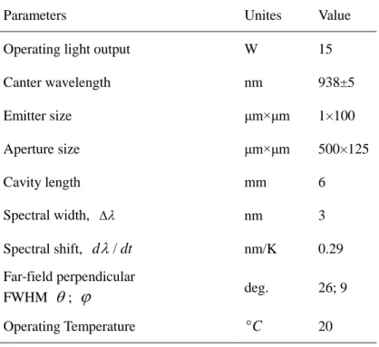
1μm×100μm in high and in wide respectively. Fig 2.5 shows the optical radiation generated by a single emitter of laser diode. Apparently, the beam let of diode radiation in z and y axis are not symmetric. The typical divergence in the fast axis z is around 30 deg. and in slow axis y is around 10 deg. at the full-width half –maximum intensity (FWHM). The single emitter diode normally can emit 1~10 W. Recently, the company of Optoenergy Inc.17 offers high-brightness single emitter diode chips with the output power over 15 W. The power is enough for achieving over hundreds watts pump by using 10 pieces diode chips or more. The advantage of these chips is: the emitter is pretty small that can be coupled directly inside the waveguide without any focus. Table 2.2 shows the specification of the diode chips offered by Optoenergy Inc. The parameters are used for our calculation and analysis in this thesis.
The far field of spacial intensity profile of the single emitter output can be approximately defined by the equation18:
2 2
0
( , , z) 2 exp[ s ]
chip
P y y z
P x y
w x x
π ϕθ − ϕ θ
= − −
(2.7)
Where, the P0 is the total output power, the (ys, 0, 0) is the location of the emitter. The θ and ϕ are the far-field perpendicular FWHM divergence angels of the fast axis and slow axis showed in Fig.2.5. The relationship between FWHM width and 1 / e2 width can be given by:wFWHM =w1/e2 2Ln(2).
The diode bar is consisted by several of diode emitter in linear array. Normally, the number of the emitter is 5~20. The commercial diode bar typically can supply the total power over 100 W in CW operation around 940 nm with the emitter number around 12. The aperture size is about 12mm×0.125mm, if use these bars as edge-pumped source, the lens is needed for the collimation and coupling corresponding the smaller core size. One special type diode mini bars are offered by Optoenergy. Inc. The mini bare has the aperture size about 3.5mm×0.125mm with the total power of 80 W from 7 emitter. This size is small enough to pump into the microchip without any focus by lens.
Table 2.2 The specification of single emitter diode chip
Parameters Unites Value
Operating light output W 15
Canter wavelength nm 938±5
Emitter size μm×μm 1×100
Aperture size μm×μm 500×125
Cavity length mm 6
Spectral width, ∆ λ nm 3
Spectral shift, dλ/dt nm/K 0.29 Far-field perpendicular
FWHM θ; ϕ deg. 26; 9
Operating Temperature °C 20
The far field intensity distribution of a beam generated by the diode bar can be described by:
0
0 0
( , , ) 1 2
y
bar y chip s
P x y z P dy
y −
=
∫
(2.8)where the 2y0 is the length of the bar aperture. Figure.2.6 shows the far-filed intensity profile generated by one mini bare mentioned above. In the picture show the intensity profile at distances of, 0.2 y0 0.5 y0and y0.Using the parameters:θ and 1/e2
1/e2
ϕ with the number of 39.6 deg. and 15.1 deg. respectively. The intensity profile
becomes uniform after the distancey0.
In many cases, the diode bars are stacked so called diode stacks in order to emit very high output power, over several hundred watts or even thousand watts. The pump power is pretty high and with good pre-collimation of micro-lens. In our laboratory, we have the 4 diode stacks pumped type A microchip laser modules, each of the diode stacks can emit over 250 W at CW operation by 6 diode bars stacked. The pump intensity profile after collimation and focusing is roughly a top-hat shape.
a c abs
η η η= , where the η is the coupling efficiency described by c ηc =Pin/Pp, the
ratio of the power coupling inside the laser material with the total pump power.
1 exp( )
abs dp
η = − −α , α is the absorption coefficient and d is the propagation p distance of pump beam inside laser material. In the edge-pumped microchip situation, the pump beam propagate in the laser materials by total internal reflection, the thickness l far less than the diameter of laser material 2r. It could be approximately replace the dp by 2r for the most simple case. As the shape of laser core is round shape, the dp varies in different incident position. We used for the width of top-hat pump beam (the laser stacks or laser bar situation), by neglecting the ϕ (for micro 1/e2
lens collimated stacks, only less than 1 deg. and the beam path in the laser material only several millimetres) η can be written as: abs
2 2
2
,
(1 )
( 2 , / 2; 2 , )
s s
y r y
y abs T
s s
e dy
d
d r y d d r y r
α
η
− −
− −
=
≤ = > =
∫
(2.9)the coordination follows that in Fig.2.4 and incident direction is along the -x axis. Figure.2.7 shows the absorption efficiency η as a function of the absorption a coefficient α . We assume η =1 and the Type A microchip situation, which r=1.5 c mm under the condition of different pump width d=0 mm, d=1 mm, d=2 mm, d =2.5 mm. d =3mm and d=4mm. Base on the result, it is easy to find if the pump width d is same or bigger than the diameter 2r, the absorption efficiency is not so good. It is better to keep the ratio r/d>0.6,
2 2 2
/ 2 2
/ 2 2
, 2
2
(1 ) [ 2 ]
[ 2 ]
r r y
r
r abs G
r
e Exp y dy
w Exp y dy
w
α
η
− −
−
∞
−∞
− −
= −
∫
∫
(2.10)The coordination follows that in Fig.2.5 and incident direction is along the -x axis. Fig.2.8 shows the absorption efficiency η as a function of the absorption coefficienta α . We assume η =1 and the Type B microchip situation, which r=1.5 mm under the c condition of different pump waist wr=0 mm, wr=0.5 mm, wr =1 mm, wr =1.5 mm. wr
=2 mm and wr =3mm. Base on the result, it is easy to find if the pump waist is same or bigger than the diameter r, the absorption efficiency is not so good. It is better to keep the ratio r w/ r>1.5,
If the edge of microchip is un-coated, the coupling efficiency η can be simply c calculated by ηc = − −1 (n 1) / (2 n+1)2, where the n is the refractive index of YAG. By using n=1.82, the calculation result is about 91.5%. In reality, the η is strongly c depends on the optical design and collimated technique. As an example of diode stacks pump module for microchip Type A, the pump scheme is shown in Fig.2.9, the pump source is a 6 bar stacked diode with the fast-axis collimation microlens (made by JENO OPTIK). The full beam divigence angle after the microlens is 2
1/e 0.5
ϕ =
and θ1/e2 =12 for the slow and fast axis at the 1 / e2 intensity. The focus lens unit including a slow-axis (SA) lens and a fast-axis (FA) lens with the focus length of 30 mm and 8.5 mm respectively. These lenses are specially designed aspheric cylindrical lenses, which can foucs the pump beam to the size around 100 μm in the direction of axis z and 2~2.5 mm size in the direction of axis y with the typical distance in the Fig.2.9. This is small enough to coupling inside the l=200 μm thickness of microchip. By carefully adjust the distance and hights of the lens unit, it possible to coupling inside the microchip with ηc >90% ideally. In fact, the measurement result is around
Chapter 2
31
R and total laser cavity photo number Φ to analyse the mode competition as the equation below:
0
,
( ) ( , , )
2 ( , , )
( )
1 ( , , )
u l f p l
c
A i T
u l f
B
f f Rr x y z N
l x y z dv L
f f c
n x y z
n
σ τ φ
τ σ φ
+ − =
+ + Φ
∫∫∫
(2.17)Where φB( , , )x y z is normalized spatial distribution of the 1st mode (1st mode oscillated mode in laser cavity). φA( , , )x y z is normalized spatial distribution of the 2nd mode (2nd oscillated mode in laser cavity). In quasi-four-level laser material, the
0
Nl
− is re-absorption loss term, which is important to prevent the secondary mode reaching threshold. By numerically solve the equation 2.17, we can figure out the mode selection details including the threshold, input and output power. For better understanding of mode control theory, the flowchart of mode selection in quasi-four-level laser material is given in Fig.2.12.
Take the fundamental mode TEM00 selection as an example, the normalized spatial distribution of the laser photons φ0( , , )x y z for TEM00 and TEM10 mode can be given by:
2 2
00 2 2
2 2( )
( , , ) exp[ ]
l l
x y
x y z
w l w
φ =π − + (2.12)
2 2
2
10 2 2 1
1 2( ) 2
( , , ) exp[ ] ( )
l l l
x y x
x y z H
w l w w
φ =π − + ⋅ (2.13)
Where Hn is the Hermite polynomial with the order n, we assume the wl is beam waist of laser, which is approximately constant in the z-axis, because the thickness of microchip l is very small. Several normalized spatial distribution of the pump energy
( , , )
r x y zp can be expressed as:
2
( , , ) 1 ,
T p
p
r x y z r w
πw l
= ≤ (for top hat) (2.14)
Chapter 2
33
(the left figure (a));
, 00 th TEM
PT is the threshold of TEM00 mode under the condition of top-hat pump shape (the right figure (b)). For the area rin <1, the calculation is made by Φ =0, and, φA( , , )x y z =φ10( , , )x y z which means no cavity mode reaches the threshold before TEM10 mode. The result of the line date means if the loss of TEM10
mode is much smaller than TEM00 mode, TEM10 mode is possible to oscillate firstly before TEM00 mode. In most of the Gaussian pump case; it is quite difficult to realize this as shown in the left figure A area. This is also the reason that why traditional pump method is difficult to realize efficient high-order mode oscillation. In the right figure (b) A' area, it is much easier to realize TEM10 mode as rin <1.
For the area rin >1, the calculation is made by Φ >0, φA( , , )x y z =φ10( , , )x y z and φB( , , )x y z =φ00( , , )x y z , which means TEM00 mode reaches the threshold before TEM10 mode and make single transverse mode oscillation as in the area D and D'. The area D and D' show us the scalability of TEM00 mode in certain cavity. By the given cavity with the given loss factor Γ <1.3, the top-hat shape pumping has the difficulty in power scaling compared with Gaussian shape pump. Because soon it will reach the C and C' area, which means the TEM10 will reach the threshold and become multi-mode oscillation. For example, as Γ =1.25, the TEM10 will reach the threshold as the pump power is 2.78 times of the threshold pump. In the Gaussian pump situation, this number almost infinite. The meaning of result in this figure is limited, only in the condition of not high-power and ideal pump shape like Gaussian or Top-hat.
In the condition of high power laser, for example of thin disk mode-locked laser, the Gaussian pump shape is too sharp and it will lead to thermal problems: such as optical distortion and thermal-induced stress, we will discuss it in next chapter. Normally, the fiber coupled high-power diode produce a supper-Gaussian pump shape with the factor q=4~6. The experienced pump size is a=1.1. Then we modify the
Chapter 2
35
theory based on various pump shape. We use TEM00 mode selection as an example for better understanding and solving our practical research problems. Now it is clear that the intensive edge absorption goes against the fundamental mode generation and power scaling. In order to overcome this difficulty, we will study on the pump distribution design in edge-pumped scheme in the following chapter.
1T. H. Maiman, "Stimulated optical radiation in ruby", Nature 187, 493 (1960)
2http://www.rp-photonics.com/laser_applications.html.
3W. Koechner, Solid-State Laser Engineering, 4th ed. (Springer, 1996).
4Giesen, A., et al. "Scalable concept for diode-pumped high-power solid-state lasers." Applied Physics B 58.5 (1994): 365-372.
5Rutherford, Todd S., et al. "Edge-pumped quasi-three-level slab lasers: design and power scaling." Quantum Electronics, IEEE Journal of 36.2 (2000): 205-219.
6Taira, Takunori, William M. Tulloch, and Robert L. Byer. "Modeling of quasi-three-level lasers and operation of cw Yb: YAG lasers." Applied optics 36.9 (1997): 1867-1874.
7Saikawa, Jiro, et al. "Tunable frequency-doubled Yb: YAG microchip lasers." Optical Materials 19.1 (2002): 169-174.
8Hiroshi Sakai, Hirohumi Kan, and Takunori Taira, ">1 MW peak power single-mode high-brightness passively Q-switched Nd3+:YAG microchip laser," Opt. Express 16, 19891-19899 (2008)
9Rutherford, Todd S., et al. "Edge-pumped quasi-three-level slab lasers: design and power scaling." Quantum Electronics, IEEE Journal of 36.2 (2000): 205-219.
10Ikesue, Akio, et al. "Fabrication and Optical Properties of High Performance Polycrystalline Nd: YAG Ceramics for Solid State Lasers." Journal of the American Ceramic Society 78.4 (1995): 1033-1040.
11Kaminskii, A. A., et al. "Micro hardness and fracture toughness of Y2O3 and Y3Al5O12 based nanocrystalline laser ceramics." Crystallography Reports 50.5 (2005): 869-873.
12Tsunekane Masaki, and Takunori Taira. "High-power operation of diode edge-pumped, composite all-ceramic Yb:Y3Al5O12 microchip laser." Applied physics letters 90 (2007): 121101.
13Azrakantsyan, M., et al. "Yb3+: YAG crystal growth with controlled doping distribution." Opt. Mater. Express2 (1) (2012): 20-30.
14Masaki Tsunekane and Takunori Taira, "300 W continuous-wave operation of a diode edge-pumped, hybrid composite Yb:YAG microchip laser," Opt. Lett. 31, 2003-2005 (2006)
15Pawlowski, Edgar, et al. "Yb: YAG composite ceramic laser." Proceedings of SPIE.Vol. 7578. 2010.
16Tsunekane, Masaki and Takunori Taira. "Design and performance of compact heatsink for high-power diode edge-pumped, microchip lasers." Selected Topics in Quantum Electronics, IEEE Journal of 13.3 (2007): 619-625.
17http://www.optoenergy.com/global/index.html.
18Copeland, Drew A., and John Vetrovec. "Gain tailoring model and improved optical extraction in CW edge-pumped disk amplifiers." SPIE LASE. International Society for Optics and Photonics, 2012.
19Nicola Coluccelli, "Nonsequential modeling of laser diode stacks using Zemax: simulation, optimization, and experimental validation," Appl. Opt. 49, 4237-4245 (2010)
20Kubodera, Kenichi, and Kenju Otsuka. "Single transverse mode LiNdP4O12
slab waveguide laser." Journal of Applied Physics 50.2 (1979): 653-659.
21Shealy, David L., and John A. Hoffnagle."Beam shaping profiles and propagation."Optics & Photonics 2005. International Society for Optics and Photonics, 2005.
Chapter 3
Compact multi-direction edge-pumped
laser module
Related paper:
W. Kong and T. Taira, "Lens-less edge-pumped high power microchip laser," Appl. Phys. Lett., vol. 100, no. 14, pp. 141105-1-4 (2012)
3.1 Introduction
There are several key techniques for high-power mode-locking laser, such as cavity design, semiconductor saturable absorber mirror (SESAM), chirped mirror and so on1. Before that, the first step is to build the compact laser module suitable for TEM00 mode generation. The edge-pumped scheme exhibits advantages for high-power compact DPSSL module, but it also has the drawback that non-uniformity of pump and edge-peak pump shape. At the end of last chapter, the reason has been explained that top-hat or basin pump shape is not suitable for fundamental mode generation and power scaling. The aim of this chapter is trying to change the pump shape towards Gaussian or Super-Gaussian by theory manipulation and experimental proof.
3.2 Pump distribution design
We choose the diode chips as our pump source. The specification of diode bare-chip is shown in Talbe2.1. The output distribution is shown in equation 2.7. We assume that the pump only travels once in the laser material; refraction and scatting
are not considered at the boundary between the core and the clad of microchip; along z-axis the pump and absorption are uniform. The simulation of absorbed pump density (W/mm3) distribution is defined by:
exp{ ( , )} ( , )
( , , ) l x yg I x y
D x y z
l
α α
= − ⋅ (3.1)
Where α is the absorption coefficient, l x yg( , )≈ r2− −y2 x is the absorption length, lis the thickness of microchip and r is the radius of microchip core.I x y( , )is the input power per unit length with the unit of W/mm at the edge of the microchip core. I x y( , )can be written as:
2
2
2 2
( , ) exp{ }
( ) ( )
p c
P y
I x y
w x w x
π η
=− (3.2)
We assume the pump beam with the total power ofPp, and Ppηcreach the edge of the core. ( ) (R ) tan( 1/ 2)
2
w x ≈ −x ϕ e , R is the clad radius of microchip, 2
ϕ1/e is the
divergence angle inside the microchip. Figure 3.1 shows the pump shape by the number of (a) N=1, (b) N=3, (c) N=9 diodes from multi-directions by using the key parameter: R=4.26 mm, r=1.9 mm, α=0.3 mm-1 and 2
ϕ1/e =8.54 deg. It could be intuitively understand the concept of pump distribution design in Fig.3.1. It is the gain-guiding to realize the desired pump shape. The basic concept is to overlap the energy at the centre of microchip, which change the basin shape to the Gaussian shape. To evaluation the central peak, a very simple method is to make the comparison of the density at the centre and the core-edge of microchip, corresponding to
(0, 0, ) / ( , 0, )
D z D r z . The calculated result for Fig.3.1 (a) (b) (c) is 0.31, 0.94, 2.8, respectively.
thermal distribution, then by the thermal distribution, the stress, displacement and OPD can be addressed.
For any pump shape D x y z( , , )is related with heat load Q x y z( , , ) distribution as:Q x y z( , , )=P D x y zh ( , , ), where Ph is total heat load including the heat from the quantum defect, the absorption of pump power and fluorescence by coatings and metallization. We assume Ph is percentage of total pump power and
( , , ) 1
microchip
D x y z =
∫∫∫
.We calculate the temperature distribution by the steady state heat distribution equation and we assume the axis symmetric microchip and use polar coordinates3:
2
2
Yb
1 ( , )
( )
( , )
T T Q r z
r r r r z K T c
∂ ∂ +∂− =
∂ ∂ ∂ (3.5)
Where Q r z( , )is re-written heat load, also can be called heat source density in the microchip.K T c( , Yb) is thermal conductivity which has relationship with temperature
T and doping concentration cYb of Yb:YAG. We use the thermal and doping dependence K T c( , Yb)as shown in the Ref.4:
Y Y Y
( , c )b p( , c ) ( , c )b b K T =ρC T D T
(3.5)
where ρ is density, Cp is isopiestic specific heat for unit mass and D is thermal diffusivity. They are given by:
Yb
Yb
Yb
Y Yb
( , ) 3 ( )
( ) ( )
( , c ) ( )
p A B D
D
b
m T
C T c N k f
M c
D T A c B c
T
= Θ
= +
(3.6)
NA, kB, m, M and fD are Avogadro constant, Boltzmann constant, number of atoms in unit cell in host crystal, molecular mass and Debye function. A, B and ΘD are fitting functions.
Chapter 3
53
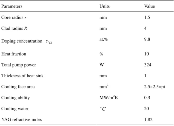
The parameters in Table 3.1 are applied for the simulation. We assume Type B for the shape of microchip. The internal heat generation is only inside the core area and along the z-axis it is uniform.
Table 3.1 The parameters for thermal simulation
Parameters Units Value
Core radius r mm 1.5
Clad radius R mm 4
Doping concentration cYb at.% 9.8
Heat fraction % 10
Total pump power W 324
Thickness of heat sink mm 1
Cooling face area mm2 2.5×2.5×pi
Cooling ability MW/m2K 0.3
Cooling water C 20
YAG refractive index 1.82
The parameters of materials are shown is Table 3.2.forthermal and structure calculation in finite element software ANSYS.
Fig.3.15 shows the temperature distribution of the top surface along the x-axis.The thermal distribution is caculated under different kind of pump shape: the idea top-hat shape and Gaussian shape, the pump shape in Fig.3.12 and Fig.3.13. The temperature distribution stronly deponds on the pump distribution and the constant temperature aear can be got when the top-hat pump shape. The radius of constant area is around 0.7r. The Gaussion shape pump has a peak of temperature at the very centre. The temperature gradiant is biggest compared with other Gaussian like pump shape. But the top-hat pump shape, at boundary of pump and unpumped area, the termperature gradiant is biggest. The termperature distribution of the pump shape in