The Si
/
CdTe semiconductor Compton camera of the ASTRO-H Soft Gamma-ray Detector
(SGD)
Shin Watanabea,b, Hiroyasu Tajimac, Yasushi Fukazawad, Yuto Ichinohea,b, Shin’ichiro Takedaa, Teruaki Enotoe, Taro Fukuyamaa,b, Shunya Furuid, Kei Genbaf, Kouichi Haginoa,b, Atsushi Harayamaa, Yoshikatsu Kurodaf, Daisuke Matsuuraf, Ryo Nakamurad, Kazuhiro Nakazawab, Hirofumi Nodab, Hirokazu Odakaa, Masayuki Ohtaa, Mitsunobu Onishif, Shinya Saitoa,b, Goro
Satog,a, Tamotsu Satoa,b, Tadayuki Takahashia,b, Takaaki Tanakah, Atsushi Togoa,b, Shinji Tomizukac
aInstitute of Space and Astronautical Science, Japan Aerospace Exploration Agency, 3-1-1 Yoshinodai, Chuo Sagamihara, Kanagawa, 252-5210, Japan bDepartment of Physics, The University of Tokyo, 7-3-1 Hongo, Bunkyo, Tokyo, 113-0033, Japan
cSolar-Terrestrial Environment Laboratory, Nagoya University, Furo, Chikusa Nagoya, Aichi, 464-8601, Japan dDepartment of Physical Science, Hiroshima University, 1-3-1 Kagamiyama, Higashi-Hiroshima, Hiroshima, 739-8526, Japan
eNishina Center, RIKEN, 2-1 Hirosawa, Wako, Saitama, 351-0198, Japan
fNagoya Guidance and Propulsion Systems Works, Mitsubishi Heavy Industry Ltd., 1200 Higashi Tanaka, Komaki, Aichi, 485-8561, Japan gResearch Institute for Science and Engineering, Waseda University, 3-4-1 Okubo, Shinjuku, Tokyo 169-8555, Japan
hDepartment of Physics, Kyoto University, Kitashirakawaoiwake, Sakyo Kyoto, Kyoto, 606-8502, Japan
Abstract
The Soft Gamma-ray Detector (SGD) is one of the instrument payloads onboard ASTRO-H, and will cover a wide energy band (60–600 keV) at a background level 10 times better than instruments currently in orbit. The SGD achieves low background by combining a Compton camera scheme with a narrow field-of-view active shield. The Compton camera in the SGD is realized as a hybrid semiconductor detector system which consists of silicon and cadmium telluride (CdTe) sensors. The design of the SGD Compton camera has been finalized and the final prototype, which has the same configuration as the flight model, has been fabricated for performance evaluation. The Compton camera has overall dimensions of 12 cm×12 cm×12 cm, consisting of 32 layers of Si pixel sensors and 8 layers of CdTe pixel sensors surrounded by 2 layers of CdTe pixel sensors. The detection efficiency of the Compton camera reaches about 15% and 3% for 100 keV and 511 keV gamma rays, respectively. The pixel pitch of the Si and CdTe sensors is 3.2 mm, and the signals from all 13312 pixels are processed by 208 ASICs developed for the SGD. Good energy resolution is afforded by semiconductor sensors and low noise ASICs, and the obtained energy resolutions with the prototype Si and CdTe pixel sensors are 1.0–2.0 keV (FWHM) at 60 keV and 1.6–2.5 keV (FWHM) at 122 keV, respectively. This results in good background rejection capability due to better constraints on Compton kinematics. Compton camera energy resolutions achieved with the final prototype are 6.3 keV (FWHM) at 356 keV and 10.5 keV (FWHM) at 662 keV, respectively, which satisfy the instrument requirements for the SGD Compton camera (better than 2%). Moreover, a low intrinsic background has been confirmed by the background measurement with the final prototype.
Keywords: Compton camera, ASTRO-H SGD, Gamma-ray detector, Semiconductor detector, CdTe detector, Silicon detector
1. ASTRO-H SGD
ASTRO-H, the new Japanese X-ray Astronomy Satellite[1, 2, 3] following the currently-operational Suzaku satellite, aims to fulfill the following scientific goals:
• Revealing the large-scale structure of the universe and its evolution.
• Understanding the extreme conditions of the universe.
• Exploring the diverse phenomena of the non-thermal uni-verse.
• Elucidating dark matter and dark energy.
In order to fulfill the above objectives, the ASTRO-H satellite hosts the following four types of instruments: SXT (Soft X-ray Telescope)+SXS (Soft X-ray Spectrometer), SXT+SXI (Soft
X-ray Imager), HXT (Hard X-ray Telescope)+HXI (Hard X-ray Imager)[4, 5, 6, 7, 8, 9, 10, 11] and SGD (Soft Gamma-X-ray Detector) [4, 5, 6, 7, 9, 12, 13, 14].
600 keV band compared with the currently operating space-based instruments.
In this paper, we will present the detailed configuration and the data acquisition system of the SGD Compton camera. We will also present the performance evaluated for the final proto-type, which is equivalent to the flight model.
2. SGD concept and Si/CdTe Semiconductor Compton Camera
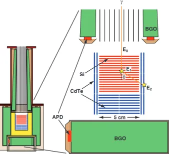
The SGD is based on the concept of narrow FOV Compton telescopes[5], combining Compton cameras and active well-type shields. The active well-well-type shield concept originates from the Hard X-ray Detector (HXD)[26] onboard the Suzaku satellite. The HXD achieves the best sensitivities in the hard X-ray band, consisting of Si photodiodes and GSO scintilla-tors with BGO active shield and copper passive collimator. The SGD, however, replaces the Si photodiodes and GSO scintilla-tors with the Compton camera, which provides additional infor-mation for the background rejection. Figure 1 shows a concep-tual drawing of an SGD unit. A BGO collimator defines a field of view of∼10◦for high energy photons while a fine collimator restricts the FOV to.0.6◦for low energy photons (.150 keV), which is essential to minimize the CXB (cosmic X-ray back-ground) and source confusion. Scintillation light from the BGO crystals is detected by avalanche photo-diodes (APDs) allowing for a compact design compared to phototubes.
The hybrid design of the Compton camera module incorpo-rates both Si and CdTe imaging detectors. The Si sensors are used as detectors for Compton scattering since Compton scat-tering is the dominant process in Si above∼50 keV compared with∼300 keV for CdTe. The Si sensors also provide better constraints on the Compton kinematics because of smaller ef-fect of Doppler broadening[27, 28]. The CdTe sensors are used to absorb gamma rays following Compton scattering in the Si sensors.
BGO
CdTe Si
APD 5 cm
E2
E0
BGO E1
Q G
Figure 1: Conceptual drawing of an SGD Compton camera unit.
3. Instrument-level requirements for SGD Compton cam-eras
The ASTRO-H mission-level science objectives described above require the SGD to provide spectroscopy up to 600 keV for over 10 accreting supermassive black holes with fluxes equivalent to 1/1000 of the Crab Nebula (as measured over the 2–10 keV band, assuming the spectrum to be a power-law with spectral index of 1.7). This mission-level science require-ment defines the following instrurequire-ment-level requirerequire-ments for the SGD Compton camera:
• Effective area for the detector must be greater than 20 cm2 at 100 keV to obtain a sufficient number of photons in a reasonable observation time (typically 100 ks).
• Observation energy range must be from 60 keV to 600 keV.
• Energy resolution must be better than 2 keV (FWHM) or better than 2% (FWHM).
There are the following design constraints on the SGD Compton camera fro mounting the ASTRO-H:
• The size of one camera must be 12 cm×12 cm×12 cm to minimize the size of BGO active shield, since the BGO is the dominant contributor to the total weight of the SGD.
• The number of Compton cameras must be six in total ASTRO-H.
• Power consumption must be lower than 6 W for one cam-era.
The instrument-level requirements and the design constraints described above guide the designs of the Si sensor, the CdTe sensor and the readout Application Specific Integrated Circuit (ASIC) for both. The detection area of the Si sensor must be larger than 5 cm ×5 cm. The total thickness of the Si sen-sor must be about 2 cm, which corresponds to the 50% inter-action efficiency for 100 keV photons. Therefore, 32 layers of Si sensors are needed when 0.6 mm thick Si devices are used. In order to satisfy the effective area requirement, CdTe sensors must cover 50% of the solid angle covered by the Si sensors. The readout ASICs for the Si and CdTe sensors must have an internal analog-to-digital converter (ADC) and must be controllable with digital signals because space in the Comp-ton camera is limited. Moreover, the ASIC must consume less than 0.5 mW/channel and have good noise performance of 100– 200 e- (ENC) under the condition that the input capacitance is several pF.
4. SGD Compton Camera Design
4.1. Overall Design
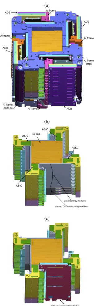
Figure 2 shows a 3D model of the Compton camera structure. This arrangement allows a placement of the CdTe sensor on the side very close to the stacked Si and CdTe sensors, maximizing the coverage of the photons scattered by the Si sensors. In ad-dition to sensor modules, the Compton camera holds an ASIC controller board (ACB) and four ASIC driver boards (ADBs). The ACB holds a field programmable gate array (FPGA) that controls the ASICs. The ADB buffers control signals from the ACB, sends control signals to 52 ASICs, and also provides a current limiter to power the ASICs.
The mechanical structure of the Compton camera needs to hold all components described above within a volume of 12×12×12 cm3. Another important requirement for the me-chanical structure is sensor cooling. All sensors need to have a temperature that is within 5◦C of the cold plate interface at the bottom of the Compton camera.
Figure 2 (a) shows the mechanical support structure of the Compton camera. The Compton Camera consists of a stack of Si and CdTe sensor trays as shown in Figure 2 (b). In addi-tion to the stack, one ”side CdTe sensor module” is installed on each side as shown in Figure 2 (c). Each ADB is attached to the side CdTe sensor module and an ACB is attached to the bot-tom frame. The material of the sensor tray structure employs polymide.
4.2. Readout ASIC for Si and CdTe sensors
The main performance requirements for an ASIC are low noise and low power. In order to satisfy these main re-quirements, the ASIC was developed based on the VIKING architecture[29, 30] which is known for good noise per-formance and has been in various space experiments like Swift[31], PAMELA[32] and AGILE[33].
Figure 3 shows the circuit diagram for the ASIC developed for the SGD (and HXI) of ASTRO-H. Each channel consists of charge sensitive amplifier followed by two shapers. One shaper with a short shaping time is followed by a discriminator to form a trigger signal. The other shaper with a long shaping time is followed by a sample and hold circuit to hold the pulse height at the timing specified by an external hold signal.
Many important functionalities are integrated in the ASIC for the SGD in order to minimize additional components re-quired to read out the signal, as shown in the circuit diagram with a blue background region. The signals in all channels are converted to digital values concurrently with Wilkinson-type analog-to-digital converters (ADCs). The conversion time is less than 100 µs. In order to minimize the readout time, the only channels that are read out are those above a data threshold that can be digitally set for each channel independently from the trigger threshold. We usually observe common mode noise from this type of ASIC at the level of∼1 keV. Common mode noise has to be subtracted to accurately apply the threshold for the zero suppression. The common mode noise level of each event is detected by taking an ADC value of the 32nd [a half of total number of channels] pulse height, corresponding to a median value of all ADC values. With zero suppression, the readout time is 0.5 µs per ASIC when no data is readout and
(a)
ADB
ADB
ADB ADB
Al frame!
(top) Al frame
Al frame Al frame
Al frame
Al frame!
(bottom)
(b)
Si sensor tray modules
stacked CdTe sensor tray modules Si pad
ASIC
ASIC
ASIC
ASIC
(c)
side CdTe sensor tray module
(9+n)µs when we readoutnchannels. Without zero suppres-sion, the readout time becomes 73µs per ASIC.
The ASIC produces all necessary analog bias currents and voltages on the chip by internal Digital to Analog Converters (DACs) except for the main bias current which sets the scale of all bias currents. Each bit of the registers for all internal DACs and other functions consists of three flip-flops and a majority selector for tolerance against single event upset (SEU). If the majority selector detects any discrepancies among three flip-flops, it will set a SEU flag which will be readout as a part of output data. The ASIC is fabricated on a wafer with an epitax-ial layer that will improve immunity against latch up. Table 1 summarizes the specifications.
Table 1: SGD ASIC specifications
Geometrical specifications
Number of channels 64
Input pitch 91µm
Thickness 0.45 mm
Analog specifications
Power consumption 0.2 mW/channel
Fast shaper peaking time 0.6µs
Slow shaper peaking time ∼3µs
Noise performance 180e−(RMS) at 6 pF load 1.5 keV (FWHM) for Si
Threshold 1500e−at 6 pF load
5.4 keV for Si
Threshold range 625 – 6250e−
Threshold step 208e−
Dynamic range ±100,000e−
360 keV for Si Digital specifications
ADC setup time 5µs
ADC power consumption 0.5–2 mW/channel
5–20µW/channel at 100 Hz
Data clock speed <10 MHz
Conversion clock speed <10 MHz (external clock)
<20 MHz (internal clock) Conversion time <100µs (external clock)
<50µs (internal clock)
Readout time (no data) 0.5µs per ASIC
Readout time (nchannels) (9+n)µs per ASIC
The data input and output circuits on the ASIC are designed to allow daisy-chaining of multiple ASICs. In one scheme, the data output of one ASIC can be connected to the input of an-other ASIC and the ASIC will pass the input data to the output via a shift register. This scheme is used to set register values. In another scheme, the outputs of several ASICs can be connected to a single bus. The output is controlled by passing a token from ASIC to ASIC. Or, in the case of trigger signal, ASICs can issue trigger signals at any time since the output circuit is open-drain FET to allow multiple triggers on the same bus. In the Compton camera, 6 ASICs (in the side CdTe tray modules)
or 8 ASICs (in the stack tray modules) are daisy chained.
4.3. Si and CdTe Pad Detector
Si and CdTe sensors are pixellated to give two-dimensional coordinates with a pixel size of 3.2×3.2 mm2. Pixel size is chosen so as to minimize the number of pixels for lower power consumption while avoiding the pixel size to be the dominant contribution to the angular resolution of Compton kinematics.
The Si pad devices are manufactured by Hamamatsu Pho-tonics K. K. Each Si sensor has 16 ×16 pixels providing 5.12×5.12 cm2 active area. A signal from each pixel on the Si sensor is brought out to one of the bonding pads at the cor-ner of the sensor by a readout electrode placed on top of the SiO2 insulation layer with a thickness of 1.5 µm as shown in Figure 4 (a). The readout electronics are DC-coupled to the Si sensor. The thickness of each Si device is 0.6 mm and the operating bias voltage is 230 V. The capacitance per pad is 4– 15 pF, including the capacitance attributed to the traces. The leakage current is about 2 nA for one device at the temperature of−20◦C .
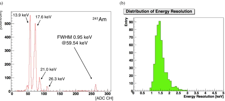
Figure 4 (b) shows the structure of the Si sensor tray mod-ule. One tray module consists of two Si pad devices and eight front end cards (FECs) with one ASIC. Sixteen tray modules are stacked in one Compton camera. The spectral performance obtained with Si sensor tray modules is shown in Figure 5. Figure 5 (a) shows the 241Am spectrum obtained with one of the best pixels. The FWHM energy resolution is 0.95 keV for 59.54 keV gamma rays at the operating temperature of−20oC. Figure 5 (b) shows the distribution of the energy resolutions ob-tained with the pixels of the Si sensors. This variation of the en-ergy resolutions result from the difference of input capacitance due to readout traces for readout signal from pixels.
The CdTe pad devices are produced and processed by ACRO-RAD Co. Ltd. The CdTe sensor has 8×8 pixels providing 2.56×2.56 cm2active area as it is difficult to fabricate a CdTe sensor much larger than 3×3 cm2. CdTe sensors are tiled in a 2×2 array for each layer in the bottom and in a 2×3 array for each layer on the side to obtain the required active area. In order to overcome small mobility and short lifetime of carri-ers in CdTe sensors, we employ a Schottky-barrier diode type CdTe sensor with Indium (In) anode and Platinum (Pt) cathode so that we can apply high bias voltage with low leakage current. The indium electrode functions as a common biasing electrode while Pt electrodes form pixels. Titanium is placed on the In electrode to reduce the resistance. Diode type CdTe sensors suffer degradation of energy resolution due to charge trapping over time (i.e. polarization). It is known that the polarization slows down at lower temperature and the effect of polarization can be reduced by applying higher bias voltage. For example, it was found that one week of operation of this type of CdTe sen-sor shows little polarization effect at<5◦C and>1000 V/mm. Moreover, this polarization effect can be recovered by turning off the bias voltage and the recovery process accelerates at a higher temperature.
ADC
VA
TA
CSA Slow shaper τ~ 2–4 µs Charge
in
6
4
ch
a
n
n
e
ls
Hold
Fixed delay Voltage
ramp
10-bit global counter
Digital threshold
ADC data
10 10 10 To common mode noise detection
Digital comparator 10-bit
ADC latch Digital delay Discriminator S/H
Trigger
out
Discriminator
Vss Fast shaper
τ~ 0.5 µs
Threshold Vdd
Figure 3: Circuit diagram of the ASIC developed for the SGD. The circuits shown in a blue background are implemented in this development.
(a) (b)
Si
Frame
Si
LSI
LSI
Wire-bonding
Wire-bonding
3.6mm
(a) (b)
241
Am
FWHM 0.95 keV
@59.54 keV
[ADC CH]
[co
u
n
t/
b
in
]
FWHM 0.95 keV! @59.54 keV
13.9 keV 17.6 keV
21.0 keV
26.3 keV
Figure 5: (a)241Am X-ray/gamma-ray spectrum obtained with a Si sensor of a Si tray module. This spectrum is obtained with one of the best pixels. The FWHM energy resolution is 0.95 keV for 59.54 keV gamma rays. The operating temperature is−20oC. (b) The distribution of the energy resolutions obtained with the
pixels of the Si sensor tray modules for 59.54 keV gamma rays. The mean energy resolution is 1.5 keV (FWHM).
of the CdTe sensor. In order to address these issues, we em-ploy a separate fanout board to route signal from each pixel to the corner of the sensor where ASICs are placed. The fanout board is made of 0.3 mm thick ceramic (Al2O3) substrate that allows fine pitch between electrodes to match the input pitch of the ASIC (91µm). The CdTe sensor and the fanout board are bonded by using a conductive epoxy as shown in Figure 6. ASIC and the fanout board are connected by wire bonding. The readout electronics are DC-coupled to the CdTe sensor.
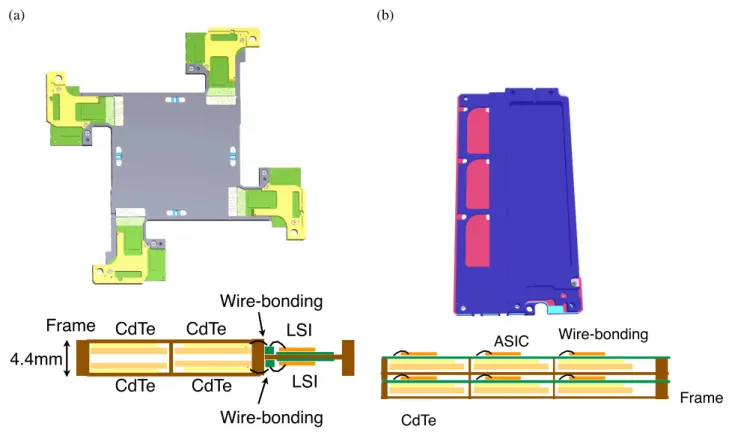
Figure 7 (a) shows the structure of the stack CdTe sensor tray module. This CdTe sensor tray module has the same outer shape as the Si sensor tray module. The stacked CdTe sensor tray module consists of two 2×2 tiled CdTe sensor arrays and eight FECs. In one Compton camera, four stacked CdTe sensor tray modules are placed underneath the Si sensor tray modules.
The side CdTe sensors surrounding the Si and CdTe stack play important roles in the SGD Compton camera. Since the Si part is tall, the side sensors are essential for covering the large solid angle of the Si sensors. Relatively low energy gamma-ray photons, such as 100–200 keV, are the main target of the SGD and these photons are the most likely to be Compton scat-tered with a large scattering angle. Moreover, these Compton scatterings with a large scattering angle provide the gamma-ray polarization information[34, 35]. Figure 7 (b) shows the struc-ture of the side CdTe sensor tray module. This module consists of two layers. CdTe sensors are tiled in an 2×3 array for each layer.
The spectral performance obtained with the CdTe sensor tray is shown in Figure 8. This is a57Co spectrum obtained with one of the best pixels. The FWHM energy resolution is 1.7 keV at 122 keV. The operating temperature is−10oC and the applied bias voltage is 1000 V.
Figure 6: The CdTe pixel sensor devices bonded with the ceramic fanout board. The left half shows the front with the ceramic fanout board for the pixels and the right half shows the common anode electrode utilizing Indium.
4.4. Readout System
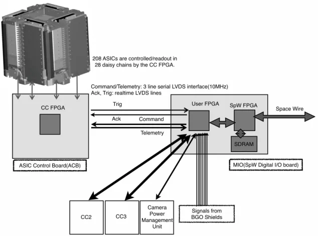
The readout system of the SGD Compton camera consists of the FECs, ADBs, ACB and MIO(Mission I/O) board as shown in Figure 9.
(a) (b)
Frame
LSI
LSI
Wire-bonding
Wire-bonding
CdTe
CdTe
CdTe
CdTe
4.4mm
Frame Wire-bonding
CdTe
ASIC
Figure 7: (a) 3D model and conceptual illustration of the stacked CdTe sensor tray module. (b) 3D model and conceptual illustration of the side CdTe sensor tray module.
0 100 200 300 400 500 600 700 0
500 1000 1500 2000
2500
FWHM 1.7 keV
@122 keV
57
Co
Figure 8:57Co spectrum obtained with the CdTe sensor tray. This spectrum is obtained with one of the best pixels. The FWHM energy resolution is 1.7 keV at 122 keV. The operating temperature is−10oC and the applied bias voltage is
1000 V.
and FECs and all digital signals are differential to minimize the electromagnetic interference. Digital signals that are not used frequently are single ended between the ADB and the ACB due to constraints on the cable pin count. The ADB detects ex-cess current of each ASIC group in order to protect ASICs from latch-ups due to highly ironizing radiation or other causes. We can recover ASICs from latch-ups by cycling the power supply. ASICs are controlled by an FPGA on the ACB (one board per Compton camera), and the ACB FPGAs are controlled by the user FPGA on the MIO board. Communication between the Compton camera and MIO is handled via 3-line (CLK, DATA, STRB) serial protocol on LVDS physical layer. We have two additional real-time LVDS lines dedicated for trigger and trig-ger acknowledgement signals.
the buffered event data in the SDRAM are pulled by a data ac-quisition computer via the Space Wire network.
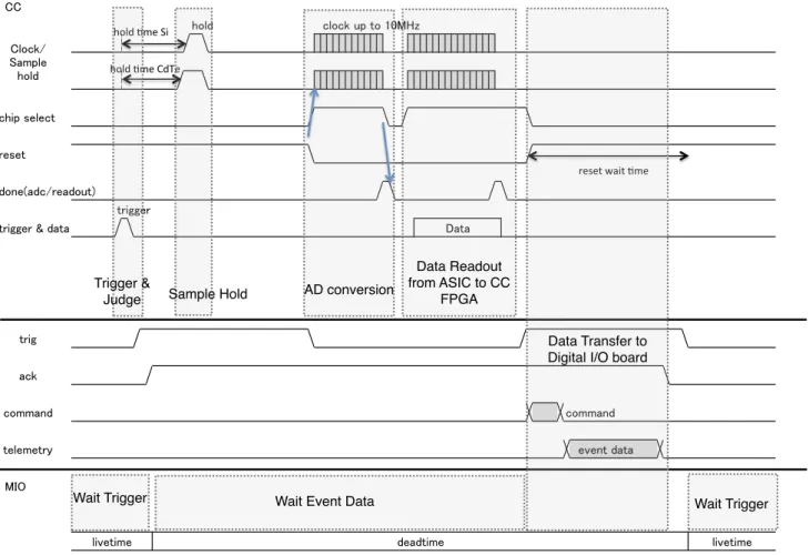
The dead-time associated with the event data acquisition is not short (100µs – several 100µs). There are two functions for more effective event data acquisitions. One is ”Trigger pattern judging”. The trigger patterns of 28 daisy chains are catego-rized into 16 groups. For each group, we can select whether the trigger is sent to the MIO or not. By using this function, we can ignore the charged particle events resulting in no related dead-time. The other function is FastBGO cancel. FastBGO is the BGO scintillator signal processed with a relatively short time interval (∼5µs) and corresponds to the relatively large en-ergy deposit in one of the BGO shields. With this function, we can cancel the event data acquisition before AD conversion by FastBGO signals, and can reduce the dead-time.
It is very important for astronomical observations to measure the dead-time accurately. To estimate the dead-time, the SGD Compton camera has a “pseudo trigger” function. This func-tion has been successfully introduced in the HXD onboard the Suzaku satellite[36]. In the SGD Compton camera system, the pseudo triggers are generated by the ACB FPGAs internally and are then processed in the same manner as usual triggers. Since the pseudo events are discarded if the pseudo trigger is generated while a “real event” is inhibiting other triggers, the dead-time fraction can be estimated by counting a number of pseudo events, output to the telemetry, and comparing with the expected counts during the same exposure. Although peri-odic pseudo triggers were used in the HXD system, the random pseudo trigger function is developed for the SGD system. A random pseudo trigger function is based on the pseudorandom numbers calculated in the FPGA and the expected count rate can be set up to 422 Hz. Random pseudo trigger function en-able us to estimate the dead-time due to the telemetry saturation in the back-end network, which can occur periodically.
5. Performance evaluation with the final prototype
5.1. Final prototype
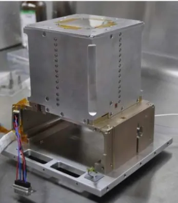
Prior to the production of the flight model, we have fabri-cated the final prototype of the SGD Compton camera. Fig-ure 11 shows a pictFig-ure of the prototype. The prototype has all the components installed in the same manner as the flight model except for some space-qualified electronic parts.
5.2. Spectral Performance
In order to evaluate the spectral performance of the proto-type, we performed gamma-ray measurement tests using var-ious radio isotopes. In the measurement tests, the prototype was operated in the temperature of about−10◦C. The prototype camera was cooled in a portable freezer and was irradiated with gamma rays by radio isotopes outside of the freezer.
133Ba and137Cs gamma-ray spectra obtained with the proto-type are shown in Figure 12. The dotted line spectra are made from the event data that can be used to reconstruct the incident gamma-ray information using Compton kinematics. The ob-tained FWHM energy resolution is 6.3 keV and 10.5 keV for
Figure 11: Picture of the final prototype of the SGD Compton camera.
gamma rays of 356 keV and 662 keV, respectively. These spec-tral characteristics satisfy the requirement for the SGD Comp-ton camera, better than 2%(FWHM).
By using the information gained from Compton scattering, we can obtain a constraint of the incident angle and can select event data from gamma rays that enter the camera directly from the radio isotope. The solid line spectra in Figure 12 are made from the event data after incident direction selection. This se-lection is performed by using the angular resolution measure (ARM) as∆θ=|θenergy−θgeom|. Here,θenergy is the Compton-scattering angle calculated from the detected energy informa-tion, and θgeom is that determined from the detected position information. The selection criteria for 133Ba and 137Cs are ∆θ < 8.4◦ and∆θ < 6.1◦, respectively. The spectral compo-nents besides emission lines are compressed with the selection, because these components are mainly generated by the gamma rays scattered by the materials around the camera and the ra-dio isotope. These results provide partial confirmation about background rejection capabilities of SGD and SGD Compton camera.
Telemetry Command Trig
Ack
MIO(SpW Digital I/O board) User FPGA
Command/Telemetry: 3 line serial LVDS interface(10MHz)!
Ack, Trig: realtime LVDS lines
Space Wire 208 ASICs are controlled/readout in
28 daisy chains by the CC FPGA.
CC2 CC3
SDRAM SpW FPGA
Signals from
BGO Shields Camera
Power Management
Unit CC FPGA
ASIC Control Board(ACB)
Figure 9: Readout system of the SGD Compton cameras.
5.3. Effective Area
The response functions for gamma-ray photons including the effective area are built with a Monte Carlo simulator. We have constructed the Monte Carlo simulator and have tuned it by adopting the measurement results from the final prototype of SGD. The details of the Monte Carlo simulators for early phase prototypes were described in [22, 37, 35, 38], and the details of the current SGD Monte Carlo simulator and event reconstruc-tion algorithm will be described in a separate publicareconstruc-tion.
The effective area based on the Monte Carlo simulator is shown in Figure 13. The effective area is defined as the prod-uct of the detector geometrical area and the detection efficiency, which is derived from the Monte Carlo simulation. The com-bined effective area for the six Compton cameras is estimated to be larger than 20 cm2 at 100 keV, and this value satisfies the instrument-level requirements for the SGD Compton cam-era. The efficiency reaches about 15% and 3% for 100 keV and 511 keV gamma rays, respectively.
5.4. Intrinsic background
Low background is the most important factor for sensitive observations with the SGD. Therefore, we performed back-ground measurements with the prototype in order to evaluate the intrinsic background generated by radio isotopes contained in the SGD Compton camera. The measurements were held in a lead cave, which works as a passive shield. This lead cave
50 60 70 100 200 300 400 500 1000
0 5 10 15 20 25
6 Compton cameras
Initial Energy[keV]
Ef
fe
ct
ive
Are
a
[cm
2] requirement
#
!
! !
"
hold%&me%Si
hold%&me%CdTe
reset%wait%&me
Data Readout from ASIC to CC
FPGA AD conversion
Sample Hold Trigger &
Judge
Data Transfer to Digital I/O board
Wait Trigger Wait Event Data Wait Trigger
Figure 10: Timing chart representing the readout sequence of the SGD Compton camera.
0 0.1 0.2 0.3 0.4 0.5 0.6 0.7 0.8 0.9 1 0
200 400 600 800 1000 1200
0 0.1 0.2 0.3 0.4 0.5 0.6
0 200 400 600 800 1000 1200 1400 1600 1800 2000 2200
before rejection
after rejection by gamma-ray direction
133
Ba
137Cs
6.3 keV(FWHM)
@356 keV
10.5 keV(FWHM)
@662 keV
Energy[MeV] Energy[MeV]
before rejection
after rejection by gamma-ray direction
∆θ < 8.4º ∆θ < 6.1º
co
u
n
ts
co
u
n
ts
Figure 12: The gamma-ray spectra of133Ba (left) and137Cs (right) obtained with the final prototype of the SGD Compton camera. The event data applicable to the Compton calculation are used for the dotted line spectra. The FWHM energy resolutions at 356 keV and 662 keV are 6.3 keV and 10.5 keV, respectively. The solid lines show the spectra obtained after the rejection by gamma-ray incident direction, which are calculated by the information of Compton scattering. The selection criteria for133Ba and137Cs are∆θ <8.4◦and∆θ <6.1◦, respectively (∆θshows the angular resolution measure as∆θ=|θ
consists of 5 cm thick lead with 1–5 cm of thick copper or brass layer inside the lead shield. The prototype Compton camera with the Pb cave was cooled to−10◦C in a thermostatic cham-ber.
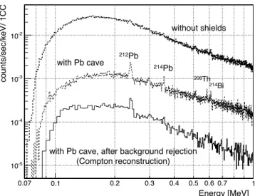
The obtained spectra are shown in Figure 14 together with the background spectrum obtained without any shields. Al-though some emission lines from the thorium and uranium de-cay series can be seen, the background level per effective area is as low as several×10−5counts/sec/keV/cm2after the Compton reconstruction. We have confirmed that there is no strong con-taminating background and will perform further measurements using BGO active shields.
Total Energy [MeV]
0.07 0.1 0.2 0.3 0.4 0.5 0.6 0.7 1
co u n ts/ se c/ ke V -5 10 -4 10 -3 10 -2 10 without shields
with Pb cave
with Pb cave, after background rejection (Compton reconstruction) 212Pb 214Pb 208Th 214Bi Energy [MeV] co u n ts/ se c/ ke V/ 1 C C
Figure 14: Background spectra obtained with the prototype SGD Compton camera. The room background spectrum obtained without any shields, the spec-trum with the Pb cave, and the specspec-trum after the Compton reconstruction are plotted.
6. Summary
We have finalized the design of the SGD Compton camera. The Compton camera has an overall size of 12 cm×12 cm×12 cm, consisting of 32 layers of Si pixel sensors and 8 layers of CdTe pixel sensors surrounded by 2 lay-ers of CdTe pixel sensors. The pixel pitch of the Si and CdTe sensors is 3.2 mm, and the signals from 13312 pixels in to-tal are processed by 208 readout ASICs with low noise and low power consumption. In order to evaluate the performance of the Compton camera, we have fabricated a final prototype, which has the same design as the flight model. The final prototype has been evaluated in the laboratory and the spectral performance, effective area and low background have been confirmed.
Acknowledgements
This work was supported by JST-SENTAN program and JSPS KAKENHI Grant Number 21684015, 24105007, 24244014, 24244021. The authors would like to thank Ms. Kirsten Bonson and Dr. Poshak Gandhi for their critical reading of the manuscript.
References
[1] T. Takahashi, et al., The NeXT X-ray mission, new exploration X-ray telescope, Proc. SPIE 7011 (2008) 14T.
[2] T. Takahashi, K. Mitsuda, R. L. Kelley, et al., The ASTRO-H mission, Proc. SPIE 7732 (2010) 77320Z–77320Z–18.
[3] T. Takahashi, K. Mitsuda, R. L. Kelley, et al., The ASTRO-H x-ray ob-servatory, Proc. SPIE 8443 (2012) 844312.
[4] T. Takahashi, K. Makishima, Y. Fukazawa, M. Kokubun, K. Nakazawa, M. Nomachi, H. Tajima, M. Tashiro, Y. Terada, Hard X-ray andγ-ray detectors for the next mission, New Astronomy Reviews 48 (2004) 269– 273.
[5] T. Takahashi, T. Kamae, K. Makishima, Future hard X-ray and gamma-ray observations, Proc. SPIE 251 (2002) 210–213.
[6] T. Takahashi, K. Nakazawa, T. Kamae, H. Tajima, Y. Fukazawa, M. No-machi, M. Kokubun, High resolution CdTe detectors for the next gen-eration multi-Compton gamma-ray telescope, in: J. E. Truemper, H. D. Tananbaum (Eds.), X-ray and Gamma-ray Telescopes and Instruments for Astronomy, SPIE, Vol. 4851, 2002, pp. 1228–1235.
[7] T. Takahashi, A. Awaki, T. Dotani, Y. Fukazawa, K. Hayashida, T. Ka-mae, J. Kataoka, N. Kawai, et al., Wide-band X-ray imager (WXI) and soft gamma-ray detector (SGD) for the NeXT mission, Proc. SPIE 5488 (2004) 549–560.
[8] M. Kokubun, et al., Hard X-ray imager HXI for the NeXT mission, Proc. SPIE 7011 (2008) 21K.
[9] M. Kokubun, S. Watanabe, K. Nakazawa, H. Tajima, Y. Fukazawa, T. Takahashi, J. Kataoka, T. Kamae, H. Katagiri, G. Madejski, K. Mak-ishima, T. Mizuno, M. Ohno, R. Sato, H. Takahashi, T. Tanaka, M. Tashiro, Y. Terada, K. Yamaoka, the HXI/SGD team, Hard X-ray and gamma-ray detector for astro-h based on Si and CdTe imaging sensors, Nucl. Instrum. Methods A 623 (2010) 425–427.
[10] M. Kokubun, et al., Hard X-ray imager for the ASTRO-H mission, Proc. SPIE 7732 (2010) 773215–773215–13.
[11] M. Kokubun, et al., The hard X-ray imager (HXI) for the ASTRO-H mis-sion, Proc. SPIE 8443 (2012) 844325.
[12] H. Tajima, T. Kamae, G. Madejski, T. Mitani, K. Nakazawa, T. Tanaka, T. Takahashi, S. Watanabe, et al., Design and performance of the Soft Gamma-ray Detector for the NeXT mission, IEEE Trans. Nucl. Sci. 53 (2005) 2749–2757.
[13] H. Tajima, et al., Soft gamma-ray detector for the ASTRO-H mission, Proc. SPIE 7732 (2010) 73216–773216–17.
[14] S. Watanabe, et al., Soft gamma-ray detector for the ASTRO-H mission, Proc. SPIE 8443 (2012) 844326.
[15] H. Tajima, T. Kamae, S. Uno, T. Nakamoto, Y. Fukazawa, T. Mitani, T. Takahashi, K. Nakazawa, Y. Okada, M. Nomachi, Low noise double-sided silicon strip detector for multiple-Compton gamma-ray telescope, in: J. E. Truemper, H. D. Tananbaum (Eds.), X-ray and Gamma-ray Tele-scopes and Instruments for Astronomy, SPIE, Vol. 4851, 2002, pp. 875– 884.
[16] H. Tajima, Gamma-ray polarimetry, Nucl. Instrum. Methods A 511 (2003) 287–290.
[17] Y. Fukazawa, T. Nakamoto, N. Sawamoto, S. Uno, T. Ohsugi, H. Tajima, T. Takahashi, T. Mitani, T. Tanaka, K. Nakazawa, Development of low-noise double-sided silicon strip detector for cosmic soft gamma-ray Compton camera, Nucl. Instr. and Meth. A 541 (2005) 342–349. [18] S. Takeda, S. Watanabe, T. Tanaka, K. Nakazawa, T. Takahashi,
Y. Fukazawa, H. Yasuda, H. Tajima, Y. Kuroda, M. Onishi, K. Genba, Development of double-sided silicon strip detectors (DSSD) for a Comp-ton telescope, Nucl. Instrum. Methods A 579 (2007) 859–865.
[19] T. Takahashi, S. Watanabe, Recent progress in CdTe and CdZnTe detec-tors, IEEE Trans. Nucl. Sci. 48 (2001) 950–959.
[20] S. Watanabe, T. Tanaka, K. Nakazawa, T. Mitani, K. Oonuki, T. Taka-hashi, T. Takashima, H. Tajima, Y. Fukazawa, M. Nomachi, S. Kubo, M. Onishi, Y. Kuroda, A Si/CdTe semiconductor Compton camera, IEEE Trans. Nucl. Sci. 52 (2005) 2045–2051.
[21] S. Watanabe, S. Ishikawa, H. Aono, S. Takeda, H. Odaka, M. Kokubun, T. Takahashi, K. Nakazawa, H. Tajima, M. Onishi, Y. Kuroda, High en-ergy resolution hard X-ray and gamma-ray imagers using CdTe diode de-vices, IEEE Trans. Nucl. Sci. 56 (2009) 777–782.
semiconductor Compton camera, IEEE Trans. Nucl. Sci. 56 (2009) 783– 790.
[23] S. Takeda, H. Odaka, S. Ishikawa, S. Watanabe, H. Aono, T. Takahashi, Y. Kanayama, M. Hiromura, S. Enomoto, Demonstration of in-vivo multi-probe tracker based on a Si/CdTe semiconductor Compton camera, IEEE Trans. Nucl. Sci. 59 (2012) 70–76.
[24] T. Takahashi, S. Watanabe, S. Ishikawa, High-resolution CdTe detectors and application to gamma-ray imaging, Semiconductor Radiation Detec-tion Systems CRC Press (2010) Chapter 8.
[25] T. Takahashi, S. Watanabe, S. Ishikawa, G. Sato, High-resolution CdTe detectors and their application to gamma-ray imaging, Sensor Technolo-gies: Biological and Medical Sensors (2011) Chapter 14.
[26] T. Kamae, H. Ezawa, Y. Fukazawa, H. M, E. Idesawa, N. Iyomoto, et al., Astro-E hard X-ray detector, Proc. SPIE 2806 (1996) 314.
[27] R. Ribberfors, Relationship of the relativistic Compton cross section to the momentum distribution of bound electron states, Physical Review B 12 (6) (1975) 2067–2074.
[28] A. Zoglauer, G. Kanbach, Doppler broadening as a lower limit to the angular resolution of next generation Compton telescopes, Proceedings of SPIE - The International Society for Optical Engineering 4851 (2) (2002) 1302–1309.
[29] O. Toker, S. Masciocchi, E. Nygård, A. Rudge, P. Weilhammer, VIKING, a CMOS low noise monolithic 128 channel frontend for Si-strip detector readout, Nucl. Instrum. Methods A 340 (1994) 572–579.
[30] H. Tajima, T. Nakamoto, T. Tanaka, S. Uno, T. Mitani, E. do Couto e Silva, et al., Performance of a low noise front-end ASIC for Si/CdTe detectors in Compton gamma-ray telescope, IEEE Trans. Nucl. Sci. 51 (2004) 842–847.
[31] S. Barthelmy, L. Barbier, J. Cummings, E. Fenimore, N. Gehrels, D. Hullinger, H. Krimm, C. Markwardt, D. Palmer, A. Parsons, G. Sato, M. Suzuki, T. Takahashi, M. Tashiro, J. Tueller, The burst alert telescope (BAT) on the Swift MIDEX mission, Space Science Reviews 120 (3-4) (2005) 143–164.
[32] P. Picozza, et al., Pamela - a payload for antimatter matter exploration and light-nuclei astrophysics, Astroparticle Physics 27 (4) (2007) 296–315. [33] M. Tavani, et al., The AGILE mission, Astronomy and Astrophysics
502 (3) (2009) 995–1013.
[34] F. Lei, A. Dean, G. Hills, Compton polarimetry in gamma-ray astronomy, Space Science Reviews 82 (3-4) (1997) 309–388.
[35] S. Takeda, H. Odaka, J. Katsuta, S. Ishikawa, S. Sugimoto, Y. Koseki, S. Watanabe, G. Sato, M. Kokubun, T. Takahashi, K. Nakazawa, Y. Fukazawa, H. Tajima, H. Toyokawa, Polarimetric performance of Si/CdTe semiconductor Compton camera, Nucl. Instrum. Methods A 622 (2010) 619–627.
[36] M. Kokubun, et al., In-orbit performance of the hard X-ray detector on-board suzaku, Publications of the Astronomical Society of Japan Vol.59, No.SP1 (2007) 53–76.
[37] H. Odaka, S. Takeda, S. Watanabe, S. Ishikawa, M. Ushio, T. Tanaka, K. Nakazawa, T. Takahashi, H. Tajima, Y. Fukazawa, Performance study of Si/CdTe semiconductor Compton telescopes with Monte Carlo simu-lation, Nucl. Instrum. Methods A 579 (2007) 878–885.