An Approach to Reduce Over-testing of Path Delay Faults in Data Paths
Using RT-level Information
Yuki Yoshikawa, Satoshi Ohtake and Hideo Fujiwara
Graduate School of Information Science, Nara Institute of Science and Technology
Kansai Science City 630-0192, Japan
Email:{yuuki-y, ohtake, fujiwara}@is.naist.jp
Abstract
In this paper, we present an approach to reduce over- testing of path delay faults (PDFs). To reduce test gen- eration complexity, design-for-testability (DFT) techniques are used in order to make a large number of untestable PDFs in a circuit testable. For a circuit modified by a DFT technique, even if faults corresponding to untestable PDFs in the original circuit are excluded from the fault list tar- geted by test generation, unfortunately the excluded faults may still be tested by the generated tests. In our previous work, we proposed a method which identifies a subset of sequentially untestable PDFs quickly by utilizing register- transfer level (RTL) information of a circuit. In this paper, for a circuit modified by some DFT technique, we show that tests generated by our test generation scheme do not test every fault corresponding to untestable PDFs in the orig- inal circuit which are identified by our path identification method.
1. Introduction
The speed of VLSI circuits has increased in recent years. High speed circuits need delay testing to verify that a given logic operates correctly at the desired clock speed. There are several delay fault models, path delay fault (PDF) model, transition fault model, segment delay fault model and so on [1]. In this paper, we target the PDF model. A PDF models a defect as cumulative propagation delays along a path exceed a specified time, hence we apply the model to test the delay between two flip-flops (FFs). To test a PDF, consecutive vectors (two-pattern test) are required for FFs which are the starting point of the target path and the starting points of other related paths.
Consider PDFs in a sequential circuit, each PDF is classified into testable PDF or untestable PDF. Moreover, each untestable PDF is classified into combinationally
untestable PDF or sequentially untestable PDF. In general, sequential test generation takes a lot of time to identify PDFs as sequentially untestable. Hence to reduce test gen- eration complexity, design-for-testability (DFT) techniques are used in order to make a large number of sequentially untestable PDFs testable ones[8]. However this induces over-testing problem because faults corresponding to se- quentially untestable PDFs, which are never activated in normal operation, in the original circuit are tested. Over- testing causes yield loss and makes test generation time and test application time long. To reduce over-testing, faults identified as sequentially untestable PDFs in the original circuit have to be removed from target of testing. There- fore we exclude those faults from the fault list for test gen- eration. However, tests generated by the test generation still may detect the excluded faults accidentally because the generated test to detect some PDF in the fault list propa- gates transitions along several paths and may also activate other PDFs. In this paper, we show that tests generated by our test generation scheme never detect PDFs which were excluded from the fault list. Note that sequentially untestable PDFs are identified by using our path identifica- tion method [7].
For a combinational logic part, combinational test gen- eration algorithms usually identify untestable paths within practical time. In [10], a method to select testable PDFs efficiently has been proposed. The work in [9] is to find se- quentially untestable PDFs by using time expansion model at gate-level. For small scale circuits the method succeeds to identify sequentially untestable PDFs within practical time. However it is conceivable that the method takes long CPU time for large scale circuits. In our previous work [7], we identified a large number of sequentially untestable PDFs at RTL in reasonable time. We referred to the ex- tracted untestable PDFs as control-dependent untestable paths (CUPs). CUPs are identified by analyzing control signals such as load-enable signals of registers and select signals of multiplexers (MUXs). Gate-level paths between two registers are regarded as a bundle of paths at RTL,
11th IEEE European Test Symposium, pp. 146-151, May 2006.
which is referred to as an RTL path. An RTL path is a path passing through only combinational module, which starts at a primary input (PI) or a register and ends at a register or a primary output (PO). Since the number of RTL paths in a circuit is much smaller compared to the total number of gate-level paths, the identification time of CUPs is quick.
Scan design is widely accepted in industry as an effec- tive DFT method. We can enhance two-pattern testability for FFs by using standard scan technique such as skewed- load testing[2] and broadside testing [3], or by using en- hanced scan technique [4, 5]. These DFT techniques make sequentially untestable PDFs testable ones. Here in order to reduce over-testing for a circuit modified by scan de- sign, we remove sequentially untestable PDFs identified as CUPs from fault list targeted by test generation. However, some of those removed PDFs will happen to be detected by the generated two-pattern tests if they are normally gener- ated with no constraint.
We propose a method to guarantee that sequentially untestable PDFs identified as CUPs are never tested by us- ing the concept of single-port-change (SPC) two-pattern testability proposed in our previous work [7]. The con- cept of SPC was originally proposed to reduce area over- head required for DFT in [7]. In this paper, we utilize the concept to reduce over-testing. Port indicates the output of a register, i.e. an input of a combinational logic block at RTL, and it has bit width. An SPC two-pattern test changes the second vectors at only one port and sets stable for the other ports. In other words, transitions are launched at each path starting from the port whose the second vectors are changed. Therefore the generated SPC two-pattern test to detect a PDF never activate the other unexpected PDFs. In this paper, to compare reduction in over-testing for SPC two-pattern tests with that for any two-pattern tests, we adopt enhanced scan technique as DFT.
Experimental results show that our proposed method never activate PDFs which are identified as CUPs. More- over, we show that if we generate any two-pattern tests with no constraint for the same fault list, on average about 60 % of PDFs identified as CUPs are tested.
2. Target circuits and faults
An RTL design generally consists of a controller, rep- resented by a state transition graph, and a data path, rep- resented by hardware elements such as registers, MUXs and operational modules. They are connected each other by control signal lines and status signal lines. A controller controls control inputs of hardware elements (e.g., load- enable signals of registers and select signals of MUXs) in the data path. On the other hand, the status signals from the data path determine a next state and/or output values of the controller. Our target circuit is a data path. Note that
0 1 0 1 R1
R3
s0 s1 s2
s0 s1
s2 +
0 1 0 1 R2 R4
CR1
CM1
CM2
CR4
PI1 PI2
PI3
M1
M2 Controller
Figure 1. An RTL circuit.
information of control signals from a controller is analyzed in order to extract control-dependent untestable paths. Our target faults are path delay faults in the data path. Note that path delay faults on control signal lines and status signal lines are not targeted in this paper.
3. Control-dependent untestable path
From an RTL description of a circuit, we can obtain in- formation about state transitions of the controller and the control signals such as the load-enable signals of registers and the select signals of MUXs for each input vector. The select signals of MUXs decide paths to transfer data from a register to next register. The load-enable signals decide the timing of data transfer between registers. We identify RTL paths which never propagate a value from the start regis- ter to the end register within one clock period as control- dependent untestable paths(CUPs) by analyzing the infor- mation.
Let P be a set of RTL paths in a data path and now we consider whether p2 P is CUP or not. Let Rsbe the register which is the starting point of p, and let Rebe the register which is the ending point of p. Let CRs and CRe be load enable signals of registers Rs and Re, respectively. If the load enable signal of a register is equal to ’1’, the register loads a value, otherwise, holds its value. Note that if the register does not have hold function, we assume that a load enable signal line is connected to the register, and the value of that signal is always ’1’. If the starting point of p is a PI or the ending point of p is a PO, the PI or the PO is treated as a register with no hold function. Let Miand CMi (1 ∑
i∑ n) be a MUX on p and its select signal, respectively ( n is the number of MUXs on p ). Let CMki be the select signal of Mi at time k. Similarly, Let CRks and CkRe be the select signal of Rsand that of Reat time k, respectively. When Mi
selects the input on p at time k, the value of the select signal is denoted as pMi. For example, suppose that p is the RTL
Table 1. Control sigals for each state. s0 s1 s2
CR1 0 0 1
CR4 1 1 0
CM1 0 1 1
CM2 0 0 1
path R1-M1-Adder-M2-R3in Figure 1. When M1and M2
select p at time k, pM1= 0 and pM2 = 0. Let Si and Sjbe states of the controller. Siand Sjis said to be consecutive if there exists a direct transition from Sito Sj. Let(CMki,Ck+1M
i )
be a select signal pair of consecutive two states.
Definition [7]: An RTL path p is control-dependent untestable path (CUP) if either of the following two con- ditions is satisfied for any consecutive two states.
1. (CkRs,CRsk+1) = (0,°) _ (CRek ,CRek+1) = (°,0)
°: don’t care
2. _ni=1{(CMki,CMk+1
i ) 6= (°,pMi)}
(CRsk ,CRsk+1) = (0,°) shows that Rs does not load a value at the first state of consecutive two states, and the next state is don’t care._ni=1{CMi 6= (°,pMi)} means that there exist at least one MUX on p which are not selecting p at the second state.
Theorem [7]: All the gate-level paths corresponding to an RTL path p are non-robust untestable if p is CUP.
proof [7]: For the first condition of Definition [7], Rsdoes not launch a transition at Si, or Redoes not capture the re- sponse at Sj even if Rs launched a transition at Si. For the second condition, p is not selected at Sj and this prevents propagation of transitions from Rs to Re. Therefore, p is
non-robust untestable. □
We consider the RTL path R1-M1-Adder-M2-R3and R1- M1-Adder-M2-R4in Figure 1 as an example of path identi- fication of CUPs. First we consider R1-M1-Adder-M2-R3. R3does not have hold function. We assume that R3has a load-enable signal line, and the signal is always ’1’. The controller has three consecutive two states (S0,S1), (S1,S2) and (S2,S0). For (S0,S1) and (S1,S2), the first condition of Definition [7] are satisfied because CR1 is zero at S0and S1
from Table 1. For (S2,S0), both the first condition and the second condition are not satisfied. Hence R1-M1-Adder- M2-R3are not CUP.
Next we consider R1-M1-Adder-M2-R4. For (S0,S1) and (S1,S2), the first condition are satisfied. For (S2,S0), the first condition are not satisfied but the second condition are satisfied. Therefore R1-M1-Adder-M2-R4is CUP.
4. Reduction in over-testing
We expect reduction in over-testing by removing se- quentially untestable PDFs corresponding to CUPs from a fault list targeted by test generation. For a circuit modi- fied by enhanced-scan technique, any two-pattern test can be applied to FFs which are the starting points of paths. Hence we usually generate two-pattern tests for the com- binational logic block without considering any input con- straint. However such two-pattern tests still may test the removed untestable PDFs.
We reduce over-testing by using the concept of single- port-change two-pattern testability.
4.1. Single-port-change two-pattern tests
In our previous work [7], we have introduced single- port-change(SPC) two-pattern tests. SPC two-pattern tests are defined at RTL. Here a combinational logic block which forms an input cone to a register is considered at RTL. Sup- pose an RTL path passing through the cone is a target of testing. The target RTL path is referred to as on-path. An RTL path which supports propagation of transitions along the on-path is called off-path. For the input port of an oper- ational module on an on-path, one of the RTL paths passing through the other input port is an off-path (See the left pic- ture of Figure 2). If an on-path passes through some oper- ational modules, every operational module has an off-path. An SPC two-pattern test is a pair of two consecutive vec- tors which launches transitions at only the starting point of an on-path, and sets stable two consecutive vectors for the starting point of an off-path (or off-paths if there exist some off-paths).
The select signal of each MU X is selecting an on-path or an off-path during test application as shown in Figure 2. In our previous method [6], we showed that while the se- lect signal of a MUX is fixed, propagation of signals from the selected input port to the output port is independent of signals at the other input port. Therefore the on-path is testable if SPC two-pattern tests can be applied to starting point of the on-path and the off-path. Test generation of SPC two-pattern tests for a combinational logic block are performed by using a combinational test generation algo- rithm with constraints. With regard to quality of SPC two- pattern tests, we showed that there always exists an SPC robust (resp. non robust) test for a robust (resp. non-robust) testable path delay fault. For functionally sensitizable path delay faults, SPC two-pattern tests can test a subset of func- tionally sensitizable path delay faults. The detail of test generation and quality of SPC two-pattern tests are shown in [7].
V12
V11
V21 V21
0 1 11 0 1 00 0 1 11
on-path off-path
V21 V21
V12
V11
V12 V11 V21
V21
Figure 2. SPC two-pattern test.
+
R1 R2
R3 V12 V11
V22 V21
Figure 3. A simple RTL structure.
4.2. Test generation and test application
Here we first explain a case where sequentially untestable PDFs removed from a fault list are tested by generating two-pattern tests. Figure 3 shows a simple RTL structure and there are two RTL paths, R1-Adder-R3 and R2-Adder-R3. We assume that R1-Adder-R3 is not a CUP and R2-Adder-R3 is identified as a CUP. Then gate-level PDFs corresponding to R2-Adder-R3 are removed from a fault list. For the fault list, we usually generate a set of two- pattern tests without input constraints i.e. any two-pattern tests can be generated. Let the first vectors for R1 and R2 be V11and V21, respectively. Let the second vectors be V12and V22, respectively. During test application, transitions may be launched at the starting point of R2-Adder-R3 because V21and V22can be different vectors. Therefore unexpected PDFs may be tested.
Next, we show that the removed untestable PDFs are never tested by generating SPC two-pattern tests. We con- sider the same fault list as the above instance. For the fault list, we generate a set of SPC two-pattern tests. During test application, transitions are never launched at the start- ing point of R2-Adder-R3 because V21and V22are the same vectors. Therefore the removed PDFs are never tested.
In this paper, we adopt enhanced scan design. Note that if we consider other DFT techniques such as non-scan DFT techniques or broadside technique and skewed-load tech- nique with standard scan, we have to consider incidental activation during justification of test patterns.
Testable paths Untestable paths
Testable paths Comb untestable Original
After ES (Any two-pat)
All the paths in the circuit
Testable paths Comb untestable unknown
known
After ES (SPC two-pat)
CUP Tested Untested
Testable paths Comb untestable After ES
Untested Tested
Tested
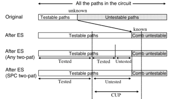
Figure 4. The ratio of CUPs to tested paths.
Table 2. Circuit characteristics.
Circuit BW #PIs # POs # REGs # RTL paths # Gate paths
Paulin 8 2 2 7 29 58,788
LWF 8 2 2 5 19 1,383
Tseng 8 3 3 6 20 8,266
JWF 8 5 5 14 153 13,000
MPEG 8 7 16 241 651 -
5. Experimental results
In this section, we evaluate the effectiveness of identi- fication of CUPs and the ratio of reduction in over-testing by using the concept of SPC two-pattern testability. In this experimental results, we adopt enhanced scan design in or- der to evaluate the difference between the ratio of reduc- tion in over-testing by using SPC two-pattern tests and that by using any two-pattern tests. The circuit characteristics of RTL benchmarks used in the experiments are shown in Table 2. Paulin, LWF, Tseng, JWF are widely used bench- mark circuits described at RTL. MPEG is more practical and larger circuit provided by industry. Generally if bit width of signal lines in a circuit increase, the circuit scale becomes large, i.e., the number of paths in the circuit expo- nentially increases. In this experiments, we need to know the total number of paths to analyze the ratio of reduction in over-testing. Hence we use 8 bit width benchmarks. How- ever, even if the bit width of signal lines increases, the CPU time required for identifying CUPs and the number of RTL paths identified as CUPs do not change. This is because the path identification method uses only the information of control signals. Moreover, the number of gate-level paths identified as CUPs increases if circuit scale becomes large. Figure 4 shows that the ratio of PDFs corresponding to CUPs to tested PDFs among CUPs as an example. For
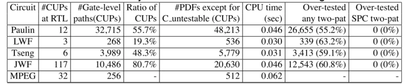
Table 3. Analysis of CUPs and reduction in over-testing.
Circuit #CUPs #Gate-level Ratio of #PDFs except for CPU time Over-tested Over-tested at RTL paths(CUPs) CUPs C untestable (CUPs) (sec) any two-pat SPC two-pat
Paulin 12 32,715 55.7% 48,213 0.046 26,655 (55.2%) 0 (0%)
LWF 3 268 19.3% 536 0.030 339 (63.2%) 0 (0%)
Tseng 6 3,989 48.3% 5,779 0.031 3,413 (59.1%) 0 (0%)
JWF 117 10,486 80.7% 20,630 0.046 12,543 (60.8%) 0 (0%)
MPEG 32 256 - 512 0.062 - -
all the PDFs in an original circuit, we cannot perform se- quential test generation within practical time. Hence we do not know the ratio of testable PDFs to untestable PDFs in the circuit exactly. However we know the ratio of testable PDFs to combinationally untestable PDFs after modifica- tion by enhanced scan design. The ratio of testable PDFs increases because sequentially untestable PDFs become testable. CUPs are a subset of sequentially untestable PDFs in the original circuit. Note that the sequentially untestable PDFs judged as CUPs may overlap with combinationally untestable PDFs. If we normally generate any two-pattern tests, some PDFs corresponding to CUPs are tested (See the third graph in Figure 4). On the other hand, our proposed method never test all the PDFs corresponding to CUPs.
Table 3 shows analysis of CUPs and reduction in over- testing. The second column is the number of RTL paths judged as CUPs in benchmarks. The third column is the number of gate-level paths corresponding to CUPs. The forth column is the ratio of the number of paths identi- fied as CUPs to the number of total paths. The fifth col- umn is the number of PDFs corresponding to CUPs ex- cept for combinational untestable PDFs. Note that there are two PDFs depending on the transition, rising transi- tion and falling transition, at the start of a path for every gate-level path. The sixth is CPU time required to identify CUPs. The seventh and the last column show that the num- ber of tested PDFs in PDFs shown in the fifth column and the percentage. For JWF, 80 % of sequentially untestable PDFs are judged as CUPs within 0.1 second. For Paulin and Tseng, about 50 % of sequentially untestable PDFs are identified as CUPs within 0.1 second. On the other hand, if we perform sequential test generation for an original cir- cuit without modification by DFT, for only 100 PDFs in Paulin it takes 498 second to judge 51 PDFs as sequentially untestable. In terms of reduction in over-testing, when we generate SPC two-pattern tests for fault lists removed se- quentially untestable PDFs, the removed PDFs are never tested. However if we generate any two-pattern tests for the same fault list, about 60 % of the removed PDFs is tested (over-testing). For MPEG, there are 651 RTL paths and the total number of gate-level paths is extremely large. Hence
we just examined the CPU time required for identifying CUPs and the time was less than 0.1 second.
6. Conclusion
In our previous work, we have proposed a method to extract a large number of sequentially untestable PDFs at RTL. However even if the untestable path delay faults are removed from a fault list targeted by test generation, the generated test patterns incidentally test the removed faults. In this paper, we have proposed a method which never test PDFs identified as control-dependent untestable paths by using single-port-change (SPC) two-pattern testability. In experimental result, we showed that SPC two-pattern tests can reduce about 60 % of over-testing compared to that for any two-pattern tests.
Acknowledgment The authors would like to thank Prof. Michiko Inoue and Dr. Tomokazu Yoneda (Nara Institute of Science and Technology) for their valuable discussion and their cooperation. This work was supported in part by 21st Century COE (Center of Excellence) Program (Ubiquitous Networked Media Computing) and in part by Japan Society for the Promotion of Science (JSPS) under Grants-in-Aid for Scientific Research B(2)(No. 15300018) and for Young Scientists (B) (No.17700062).
References
[1] Angela Krstic and Kwang-Ting(Tim)Cheng, Delay Fault Testing for VLSI Circuits, Kluwer Academic Publishers, 1998.
[2] J. Savir and S. Patel, “Scan-based transition test,” IEEE Trans. on CAD, Vol. 12, No.8, pp. 1232-1241, Aug. 1993.
[3] J. Savir and S. Patel, “Broad-side delay test,” IEEE Trans. on CAD, Vol. 13, No.8, pp. 1057-1064, Aug. 1994.
[4] B. I. Devadas and G. E. Stong, “Design for testabil- ity:Using scanpath techniques for path-delay test and
measurement,” Proceeding of International Test Conf, pp. 365-374, 1991.
[5] Tapan J. Chakraborty, Vishwani D. Agrawal, Michael L. Bushnell:“Design for testability for path delay faults in sequential circuits,” Proc. DAC 93, pp. 453- 457, 1993.
[6] Md. Altaf-Ul-Amin, S. Ohtake and H. Fujiwara, “De- sign for hierarchical two-pattern testability of data paths,” IEICE Trans. on Information and Systems, Vol. E85-D, No. 6, pp. 975-984, Jun. 2002.
[7] Y. Yoshikawa, S. Ohtake, M. Inoue and H. Fujiwara,
“Design for Testability Based on Single-Port-Change Delay Testing for Data paths,” Proc. Asian Test Symp, pp. 254- 259, Dec. 2005.
[8] T. J. Chakraborty, V. D. Agrawal, M. L. Bushnell,
“Design for Testability for Path Delay Faults in Se- quential Circuits,” Proc. 30th ACM/IEEE Design Au- tomation Conference. pp. 453-457, 1993.
[9] A. Krstic. S. T. Chakradhar, K. T. Cheng, “Testable Path Delay Fault Cover for Sequential Circuits,” Proc. European Design Automation Conference. pp. 220- 226, Sep. 1996
[10] M. Reddy, I. Pomeranz, S. Kajihara, “On Selecting Testable Paths in Scan Designs,” Proc. European Test Workchop. 2002.