RedSOCs-3D: Thermal-safe Test Scheduling for
3D-Stacked SOC
Fawnizu Azmadi Hussin#1, Thomas Edison Chua Yu#2, Tomokazu Yoneda#3, and Hideo Fujiwara#3
#1Electrical & Electronics Engineering Department, Universiti Teknologi PETRONAS Bandar Seri Iskandar, 31750 Tronoh, Perak, Malaysia
#2,#3Graduate School of Information Science, Nara Institute of Science and Technology, Takayama, Ikoma, Nara, Japan
#2[email protected] (Currently working at Renesas Electronics)
#3{yoneda,fujiwara}@is.naist.jp
Abstract—This paper investigates the challenges of a 3D-stacked system-on-chip testing, especially in terms of thermal problem. It is known that test power can be more than twice the intended power dissipation of the chip in the functional mode, for a single die. This problem is exacerbated when more than one dies are stacked on top of each other in a single package. Without proper test strategies, the thermal limit could be exceeded during test and this could permanently damage the possibly good chips. Using a heuristic approach, we proposed a set of rules that need to be followed when scheduling the core tests of each chip layer. These rules are based on the initial findings of 3D-chip test simulation using a commercial thermal simulation tool. Using these simple rules, it was found that up to 40% reduction in the peak temperature can be achieved when the thermal-aware test scheduling technique is employed.
Keywords—stacked-chip testing, thermal-aware test scheduling, 3D chip testing.
I. INTRODUCTION
VLSI manufacturing and packaging technologies have greatly improved to answer the need for smaller, cheaper, cooler and more reliable chips. One of the latest revolutionary design techniques is called System-in-a-package, or SiP. SiP design allows multiple independently designed and fabricated dies to be integrated inside a single package. Each die can by itself be a complete system-on-a-chip (SOC), consisting of multiple embedded functional cores. The most common packaging technique is to arrange the dies stacked on top of each other (3D stacking) to minimize the form factor. This design technique brings about problems on cooling and packaging, especially during the testing phase. While testing, power and heat dissipation is much greater than during normal operation and can lead to physical damage, soft errors, and finally, yield reduction.
Up to now, simply limiting test power dissipation has been the accepted approach to preventing overheating [1-3] but recent findings have shown this to be insufficient, especially for state-of-the-art chips [4, 5]. This is because besides power, factors such as package, cooling method, and circuit layout must be taken into consideration. Therefore, we explore the utilization of a temperature-aware test scheduling for the three-dimensional stacked die chips.
In the last three years, several research papers have been presented on the test of through-silicon-via (TSV)-based 3D
stacked IC (SIC) chips. 3D SIC chips are either TSV-based (Figure 1) or based on flip-chip technology, where each die layer is fabricated independently and the inter-die interface go through the I/O pads and wire bonds. In this work, both types of 3D chips are applicable.
Figure 1: A conceptual view of a 3D IC chip, with a through-silicon-via (TSV) used as interconnect between two dies or wafers [6].
Wu et al. [6] in 2008 presented an optimization technique for minimizing the test time for 3D core-based SOCs under constraints on the number of TSVs and the test access mechanism (TAM) bit width. The difference from the earlier works [1-3] is that the number of available TSVs is included as an additional constraint in the test scheduling. The TSVs are used as part of the TAM wires that connect two adjacent device layers. Only the bottom-most layer has PI/PO interfaces to the automatic test equipment (ATE). Jiang et al. [7] in 2009 studied 3D-aware test access mechanisms by taking pre-bond test times into account to optimize the overall test time.
Marinissen [8] in 2010 highlighted the challenges with respect to test contents, wafer-level probe access and the design-for-test (DFT) infrastructure required for wafer-level and package-level tests of 3D-SICs. Questions like “Should we test the TSVs already before the actual bond to the next layer is made?” and “How to test the interconnects if DFT is not fully present in both layers?” are explored. In addition, the challenges in probing the stacked chips are also explained and some solutions presented. These kinds of problems do not exist in single-die chips.
In the most recent paper in April 2010, Marinissen et al. [9] presented a DFT test access architecture for such 3D-SICs that allows for both pre-bond die testing and post-bond stack
978-1-4244-7456-1/10/$26.00 ©2010 IEEE 264
2010 Asia Pacific Conference on Circuits and Systems (APCCAS 2010), December 2010.
testing. The DFT allows modular tests of various dies, the embedded IP cores, the inter-die TSV-based interconnects, and the I/Os. They also proposed dedicated probe pads for the non-bottom dies to facilitate pre-bond die testing, TestElevators for test data transportation, and a hierarchical wrapper architecture.
In this paper, we investigate the effects of the 3D-stacking of dies on the core temperatures using a thermal simulation tool, Flotherm v7.1. The tool allows us to determine an accurate temperature profile of a VLSI chip under a given test schedule. Then, we develop a simplified model for the heating phenomena and use this to develop a temperature-aware test scheduling methodology for 3D-stacked SOCs that minimizes the test application time while preventing overheating and hotspots.
It has been shown that power-aware test schedules alone cannot guarantee thermal-safety during the test phase even for a single die scenario; there is no direct correlation between the test power and the core temperature [4]. The thermal problem is compounded when multiple dies are stacked on top of each other. In this work, we utilize a test scheduling methodology that takes into consideration the thermal behaviour of the 3D- stacked chip architecture. Results show that large peak temperature reductions are achieved without sacrificing the test application time.
II. SIMULATION MODEL
Figure 2 illustrates a model of the 3D-stacked SiP consisting of two identical dies/chips. Each chip is made up of a 10-core design based on the ITC’02 benchmark circuit, d695 [10]. Each core is based on the ISCAS’85 benchmark circuit, which are in the netlist format. The layer 1 die is attached to a heat spreader, which in turn is attached to a heat sink. In the stacked SiP architecture, the second layer die is physically attached (using a special thermal-efficient glue) to the top of layer 1; there is no direct contact between the layer 2 die and the heat sink.
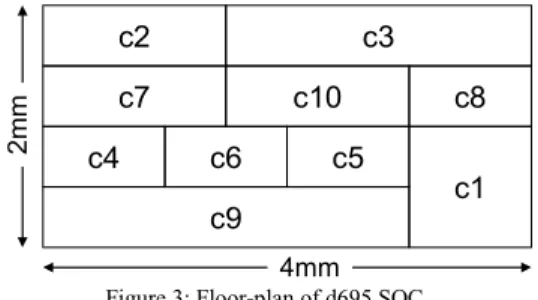
The floor-plan of the 8-mm2 rectangular chip is given in Figure 3. Core c1, for example, occupies a 1-mm2 silicon area at the bottom right corner of the design. The power dissipation of each intellectual property (IP) core used in this project is based on the number of logic signal toggling in the flip-flops [3]. The ISCAS’85 benchmark cores are in the form of a netlist, therefore we can determine the exact toggling rate of the flip-flops for given test vectors. In the example used in this project, the following design dimensions are used:
The first step of the work is to investigate the heat transfer characteristics on neighboring cores. Since simultaneous test application of multiple cores is important for reducing the test application time, we analyze the temperatures of adjacent and non-adjacent cores. For a 3D-stacked chip, we also need to consider lateral adjacency and vertical adjacency.
• Chip thickness = 0.5 mm
• Heat spreader thickness = 1 mm
• Heat spreader size = 30 mm × 30 mm
• Heat sink thickness = 6.9 mm
• Heat sink size = 60 mm × 60 mm
• Ambient temperature = 35 °C
Figure 2: Thermal simulation model with two stacked dies glued to a heat spreader and a heat sink.
c4 c2
c7 c10
c6 c5
c8 c3
c9
c1
2mm
4mm Figure 3: Floor-plan of d695 SOC.
The following simplified model in Figure 4 is used for the heat transfer analysis. Each chip consists of three identical square cores labelled c1.n, c2.n, and c3.n, where n ∈ {1, 2} is the chip layer identifier. The dimensions of each core are 1mm × 1mm × 0.1mm. In the six-core example, only one core c1.1 is active and generating heat; core c1.1 power is set to 1-Watt. During the transient simulation, we observe the temperature profiles of all cores in the circuit. The temperature plot is shown in Figure 5.
c1.2 c2.2 c3.2
c1.1 c2.1 c3.1
Figure 4: Simplified model of core-based stacked chips.
35 36 37 38 39 40 41
0.00 0.01 0.02 0.03 0.04 0.05 0.06 0.07
Time (sec)
Temperature (degC) Heat Spreader
c1.1 c2.1 c3.1 c1.2 c2.2 c3.2
Figure 5: Intra- an inter-layer heat transfer characteristics.
265
c2 c4
c5
c6
c7 c3
c10
c8
c9 c1
TAM width
Test application time Figure 6: Power-constrained test schedule.
The temperature of core c1.1 is always higher than other cores; core c1.2 temperature rises to about 88% of core c1.1’s temperature from the ambient temperature of 35 °C. The surface contact area between c1.1 and c1.2 is 1mm2. The adjacent core c2.1, whose surface contact area to the active core c1.1 is only 0.1 mm2, has a temperature increase of about 33% relative to core c1.1. This observation shows that the temperature effect on the adjacent layer is greater than its effect on the adjacent core in the same layer. This is due primarily to the size of the surface contact area between the respective cores.
In the test scheduling schemes proposed up to now, only the effect on the adjacent cores are considered [5, 11, 12]. For 3D SICs, TAM and test time minimization schemes have also been introduced [6,7]. However, the unique contribution of this paper is that we study the specific thermal effect of packaged SIC chips during testing. We offer thermal simulation results and detailed analyses of a case study for a theoretical 3D SIC based on a benchmark circuit (d695). We also offer some guidelines for test scheduling that prevents overheating of chips during testing. In the next section, we look at some of the proposed test schemes and show the corresponding experimental results to verify the effectiveness of the proposed scheme.
III. EXPERIMENTAL RESULTS
The thermal simulation was performed using Flotherm Version 7.1 software on a Windows XP running on a Core2Quad Q6600 processor with 4GB RAM. The average computation time using Flotherm for the results shown in the section is between 10 and 12 hours.
Figure 6 shows a power-constrained test schedule. Horizontal axis indicates the test time while vertical axis indicates the amount of test resources allocated to each of the core-under-test (CUT).
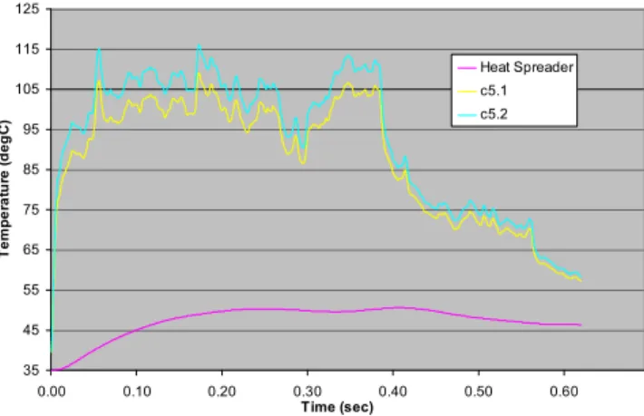
Applying the same test schedule for both chip layers simultaneously results in the temperature profile of core 5— the hottest core in the design—shown in Figure 7. The maximum temperature is approximately 116 °C. In addition, all the layer 2 cores are about 5-8 °C hotter than those in layer 1, which is attached directly to the heat-dissipating heat spreader and heat sink. This happens because the heat generated by the cores in layer 2 cannot escape as easily as those in layer 1, through the heat spreader and heat sink. This observation is useful when trying to optimize the test schedule for temperature minimization.
35 45 55 65 75 85 95 105 115 125
0.00 0.10 0.20 0.30 0.40 0.50 0.60
Time (sec)
Temperature (degC)
Heat Spreader c5.1 c5.2
Figure 7: Temperature profiles of a power-constrained test schedule.
In the proposed temperature-aware scheduling scheme, the following points are taken into consideration in the test scheduling algorithm.
• The hot cores are not tested concurrently if possible to prevent hot spots.
• The hot cores are tested at the beginning to take advantage of the lower ambient temperature.
• Adjacent cores are not tested simultaneously whenever possible.
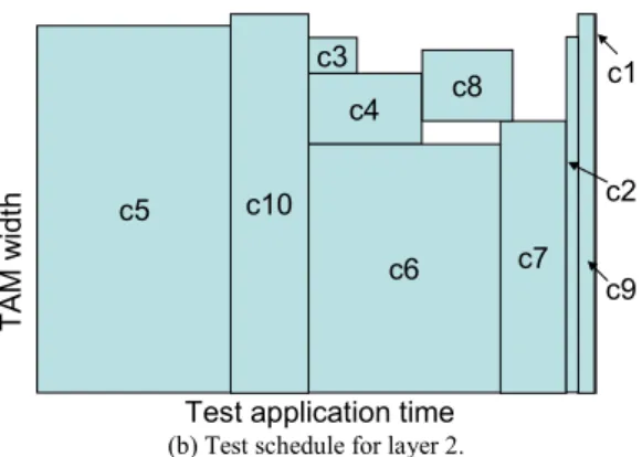
• More test resources are given to the upper layer (i.e. layer 2) in order to increase the scheduling flexibility, which would result in a more thermal-efficient test schedule. This is based on our earlier observation on the heat-dissipating capacity of the different chip layers. Figures 8(a) and 7(b) show the temperature-aware test schedules used in the thermal simulation in Flotherm v7.1. The test schedules are generated using the thermal-safe test scheduling method for a single die which we have proposed previously [5]. The main difference from the power- constrained schedule in Figure 6 is that the hottest cores are not scheduled concurrently. In addition, the core adjacency is also taken into consideration during the test scheduling. In Figure 6, several adjacent cores such as c3, c4, c5, c6, and c10 are tested simultaneously.
c4
c5
c6
c7 c3
c10 c8
c9 c1
TAM width
Test application time
c2
(a) Test schedule for layer 1.
Figure 9 illustrates the temperature characteristics for the two hottest cores—c5 and c10—utilizing the temperature- aware test schedule. Layer 1 is allocated 25% less test resources (the test access mechanism, TAM) compared to layer 2. Compared to Figure 6, the difference in the temperature profiles of identical cores in the different layers in Figure 7 is much less. This is due to the additional test resources allocated for layer 2 during the test scheduling. Overall, the peak temperature is reduced by 46 °C to about 70 °C, which is about 40% reduction.
266
c4
c5
c6 c7
c3
c10
c8 c1
TAM width
Test application time
c9 c2
(b) Test schedule for layer 2.
Figure 8: Temperature-aware test schedule for layer 1 and layer 2 chips. Different test schedules are used because of the reduced heat-dissipating
capacity of layer 2 chip.
35 40 45 50 55 60 65 70 75
0.00 0.10 0.20 0.30 0.40 0.50 0.60
Time (sec)
Temperature (degC)
Heat Spreader c5.1 c5.2 c10.1 c10.2
Figure 9: Temperature profiles of a temperature-aware test schedule.
These observations clearly show the benefits of the thermal aware test scheduling. However, we would like to point out that the scheduling scheme currently implemented does not take into consideration the inter layer adjacency. The test schedule for 3D-stacked SiP could be further improved if this new inter-layer constraint is added.
IV. FUTURE WORK
In the current scheduling scheme, we have not considered the inter-layer effect during the test scheduling process. Therefore, the immediate plan is to implement an integrated test scheduling scheme for multilayer SiP chips. The current scheduling scheme can be used as a starting point. Further reduction in the core temperature is expected when the inter- layer effects, as shown in Figure 5, are taken into consideration.
We also would like to consider extending the open source HotSpot simulator to support the 3D-stacked SiPs. In the current implementation, the simulator handles only a single layer design.
V. CONCLUSION
The results obtained thus far seem very promising. The 40% reduction in the peak temperature is very good. It is even more encouraging considering that the current test scheduling
scheme implemented does not yet take into consideration the inter layer adjacency. We expect that further reduction is possible with such an integrated test scheme, which specifically targets 3D-stacked designs. We are confident that the findings will spur other researches since the SiP technology is becoming popular.
Furthermore, this project targets just one type of SiP design—the 3D stacking of dies, where inter-layer interfaces are through the I/O pads and the external wire bonding. Various other types of SiP technologies can be explored. We are now creating the foundation to enable further exploration of the SiP testing.
ACKNOWLEDGMENT
This work was supported in part by Japan Society for Promotion of Science (JSPS) under Grants-in-Aid for Scientific Research (B) (No. 20300018) and in part by Nara Institute of Science and Technology under Creative and International Competitiveness Project (CICP 2007) grant. The authors would also like to thank members of the Computer Design and Test Laboratory for their feedback and comments.
REFERENCES
[1] V. Iyengar, K. Chakrabarty and E. J. Marinissen, “Test Access Mechanism Optimization, Test Scheduling, and Tester Data Volume Reduction for System-on-Chip,” IEEE Trans. On Computers, vol. 52, no. 12, pp. 1619-1632, December 2003.
[2] Y. Huang et al., “Optimal Core Wrapper Width Selection and SOC Test Scheduling Based on 3-D Bin Packing Algorithm,” Proc. of IEEE International Test Conference (ITC), pp. 74-82, 2002.
[3] S. Samii, E. Larsson, K. Chakrabarty and Z. Peng, “Cycle- Accurate Test Power Modeling and its Application to SoC Test Scheduling,” Proc. of IEEE International Test Conference (ITC), pp. 1-10, 2006.
[4] K. Skadron et al., “Temperature-aware Microarchitecture,” Proc. of the 30th Annual Int’l Symposium on Computer Architecture (ISCA’03), pp. 2-13, 2003.
[5] T. Yu, T. Yoneda, K. Chakrabarty and H. Fujiwara, “Thermal-Safe Test Access Mechanism and Wrapper Co- optimization for System-on- Chip,” Proc. of the 16th IEEE Asian Test Symposium (ATS’07), pp. 187-192, Oct. 2007.
[6] Xiaoxia Wu, Yibo Chen, Krishnendu Chakrabarty, Yuan Xi e, “Test- Access Mechanism Optimization for Core-Based Three-Dimensional SOCs”, In Proceedings of International Conference on Computer Design (ICCD), 2008, pp. 212-218.
[7] Li Jiang, Lin Huang, and Qiang Xu. Test Architecture Design and Optimization for Three-Dimensional SoCs. In Proceedings of the Design Automation and Test in Europe, 2009, pp. 220-225.
[8] Erik Jan Marinissen, “Testing TSV-Based Three-Dimensional Stacked ICs”, In Proceedings of the Design Automation and Test in Europe, 2010, pp. 1689-1694.
[9] Erik Jan Marinissen, Jouke Verbree, and Mario Konijnenburg, “A Structured and Scalable Test Access Architecture for TSV-Based 3D Stacked ICs”, In Proceedings of the VLSI Test Symposium, 2010, pp. 269-274.
[10] E. J. Marinissen, V. Iyengar and K. Chakrabarty, “A Set of Benchmarks for Modular Testing of SoCs,” Proc. of IEEE International Test Conference (ITC), pp. 519-528, 2002.
[11] P. Rosinger, B. Al-Hashimi and K. Chakrabarty, “Rapid Generation of Thermal-safe Test Schedules,” Proc. Design, Automation and Test in Europe (DATE) Conf., pp. 840-845, 2005.
[12] C. Liu, K. Veeraraghavan and V. Iyengar, “Thermal-Aware Test Scheduling and Hot Spot Temperature Minimization for Core-Based Systems,” Proc. of the 20th IEEE International Symposium on Defect and Fault-Tolerance in VLSI Systems (DFT'05), pp. 552-560, 2005.
267
![Figure 1: A conceptual view of a 3D IC chip, with a through-silicon-via (TSV) used as interconnect between two dies or wafers [6]](https://thumb-ap.123doks.com/thumbv2/123deta/5752579.27024/1.892.492.757.512.669/figure-conceptual-view-chip-silicon-tsv-interconnect-wafers.webp)