Chapter 1
Raman spectroscopy for practical characterization of single-walled carbon nanotubes in various environments
Shohei Chiashi1∗, Yoshikazu Homma2† and Shigeo Maruyama1,3‡
1 Department of Mechanical Engineering, The University of Tokyo, Japan
2 Department of Physics, Tokyo University of Science, Japan
3 Energy NanoEngineering Laboratory, National Institute of Advanced Industrial Science and Technology (AIST), Tsukuba 305-8564, Japan
Features of Raman scattering spectroscopy as a practical characterization tool of single-walled carbon nanotubes (SWCNTs) samples are reviewed. After the ba- sic introduction of G-band, D-band, radial breathing mode (RBM), and 2D-band (G’-band) peaks, chirality dependent G+, G−features, doping effect, and reso- nance energy profiles are reviewed. Kataura plot; optical transition energy vs.
RBM Raman shift; is the essential tool for the practical analysis of SWCNT sam- ple. Available experimental data and correlation are summarized as the Kataura plot. The Raman shift and transition energy shift depending on SWCNT mor- phologies such as directly-grown sample on substrates, vertically-aligned sample, horizontally-aligned sample, suspended sample, and micelle-wrapped chirality- selected samples are compared. The detailed discussion of the environmental effect on Kataura plot follows. Finally, the temperature dependence of Raman features is discussed.
Contents
1. Raman scattering spectra from SWCNTs . . . . 2
1.1. G-band . . . . 2
1.2. D-band . . . . 6
1.3. RBM peaks . . . . 7
1.4. Kataura plots . . . . 9
2. Environmental effects on Kataura plots . . . . 10
2.1. Raman shift . . . . 10
2.2. Resonance energy . . . . 13
2.3. Temperature dependence . . . . 15
3. Acknowledgments . . . . 17
References . . . . 17
1
Reminiscences of Millie
Raman spectroscopy of carbon nanotubes cannot be discussed without Millie. She has been the leader or the mentor of the initiation, development in experiment and in theory, and documentation of this research field. We have joined this exciting re- search field by the direct guidance of Millie. We witness that Millie was surprisingly kind and fair to new comers to the field. We can find so many researchers around the world who feel Millie as their direct mentor. Her initiatives, passion, and devote to science are always encouraging us and guiding us to continue research. We thank Millie for these immortal gifts.
1. Raman scattering spectra from SWCNTs
After the discovery of single-walled carbon nanotubes (SWCNTs),1,2 Raman scat- tering spectroscopy is one of the most important analytical tools.3 In Raman scat- tering spectra from SWCNT samples, the characteristic peaks appear and they come mainly from the phonon scattering. They are called the G-band, D-band, radial breathing mode (RBM) peaks, 2D-band (G’), and so on. The relevant phonons, Raman shift and scattering intensity of these peaks have been intensively studied.
Hence, Raman scattering spectroscopy provides us plentiful information of SWC- NTs. The knowledge is useful in analysis of not only SWCNTs but also the other carbon materials, especially nano-carbon materials, such as double-walled carbon nanotube, multi-walled carbon nanotube and graphene, and greatly contributes to the development of nanotechnology. The growth techniques of SWCNT sam- ples have been proposed, such as arc-discharge methods,1,2 laser-ablation method4 and chemical vapor deposition methods,5,6 and the growth techniques have devel- oped rapidly. SWCNTs with various morphologies can be realized; directly-growth on substrates,6 vertically-aligned growth,7,8 horizontally-aligned growth9 and sus- pended growth.10 At the same time, separation techniques after the growth are also developed, and we can obtain even single chiraliry SWCNT samples.11,12 As a result, the chirality dependence of their intrinsic physical properties are unveiled and it is found that they are affected by the morphology or the surrounding en- vironments. The importance of Raman scattering spectroscopy is increasing for the detailed analysis of SWCNT samples. For example, Raman scattering spectra from SWCNTs, which were synthesized by using alcohol catalytic CVD (ACCVD) method,13 are shown in Fig. 1. The G-band, which includes G+ peak, G− peak and BWF peak, D-band and RBM peaks are clearly observed. The split G-band is a characteristic feature of SWCNTs and RBM peaks are also unique to SWCNTs.
1.1. G-band
The G-band originates from an in-plane stretching mode of carbon-carbon bond in graphitic materials.14 In graphite, since the G-band comes from phonons with
E2g symmetry, which are equivalent longitudinal and transverse optical phonons at Γ point, the G-band appears as only one peak around 1580 cm−1. in the contrast to the single peak in the case of graphite or graphene, the G-band from SWCNTs appear around 1590 cm−1as multiple peaks.15 The G-band of SWCNTs composed of multiple peaks was explained to be the superposition of peaks from phonon with different symmetry, such as 2A, 2E1and 2E2modes.15 Even more complex G-band is often observed from bundled (aggregated) SWCNT samples.
Especially, two most prominent peaks among the G-band are called G+and G− peaks, and G− peak appears on the lower wavenumber side of G+ peak. Raman scattering spectra are measured from not only bundled SWCNTs but also dispersed SWCNTs in solution16 and suspended SWCNTs in air.17 The G-band of single- chirality SWCNT is measured from chirality-separated SWCNT solutions or a single suspended SWCNT, and it generally exhibits only G+ and G− peaks.18 Because the theory states that the intensity of Amode peaks are strong,19the G+ and G− are usually assigned to A symmetry phonons. The feature of G+ and G− peaks from dispersed SWCNTs in solution are investigated in detail and it is found that the intensity ratio between G+ and G− peaks depend on both dtube and the chiral angle.20
In the case of semi-conducting SWCNTs, G+and G−peaks are sharp, and they originate from LO and TO phonons at Γ point, respectively. Raman shift of G+peak (ωG+) do not depend on the tube diameter (dtube). On the other hand, that of G−
500 1000 1500
100 200 300 400
Raman Shift (cm
-1) In te n s it y ( a rb . u n it s )
ZD ƉĞĂŬƐͲďĂŶĚ '−ƉĞĂŬ
'+ƉĞĂŬ
t&
ZD ƉĞĂŬƐ
Fig. 1. Raman scattering spectrum from SWCNTs, which were synthesized by using alcohol cat- alytic CVD (ACCVD) method.13 The excitation laser wavelength was 488.0 nm (Eex= 2.54 eV).
peak (ωG−) clearly depend on the tube diameter, because of the curvature effect.21 Therefore, the difference of their Raman shift (ωG+−ωG−) is roughly expressed by the tube diameter (ωG+−ωG− =CS/dtube,CS= 47.7 cm−1nm2).22 In detail,ωG−
depends on both the diameter and chiral angle,23as shown in Fig. 2(A).
;Ϳ ;Ϳ
Fig. 2. (A) G+, G−and RBM peaks of semi-conducting SWCNTs with different chirality, taken from Ref.(20) with permission of Copyright c⃝2016, American Chemical Society. (B) G+ and G− peaks of metallic SWCNTs under the different gate voltage (Vg), taken from Ref.(24) with permission of Benjamin Hatting, et al., Phys. Rev. B,87, 165442, 30 April 2013, Copyright by the American Physical Society.
For metallic SWCNTs, sharp G+ and broad G− peaks are observed and they correspond to TO and LO phonons at Γ point, respectively. Note that earlier reference imply G+ and G− peaks correspond to LO and TO phonons even for metallic SWCNTs, respectively. The LO phonon of metallic SWCNTs is softened due to Kohn anomaly,25 and the softened and broad (asymmetric) G− peak of metallic SWCNTs is also called Breit-Wigner-Fano (BWF) peak.26 Because of the Kohn anomaly effect, the G-band of metallic SWCNTs is drastically modulated by changing the Fermi energy,25,27,28 as shown in Fig. 2(B).
The density of states of SWCNTs exhibits almost discrete energy levels due to van Hove singularity and their optical transition energy (Eii) corresponds to the energy gap between two energy states. Raman scattering spectra from SWCNTs are strongly enhanced by resonance Raman effect. If Eii is equal to the energy of incident light (Eex, incident resonance) or that of the scattered light (Eex± Ephonon, scattered resonance), Raman scattering intensity becomes large. Here, Eex+Ephonon and Eex−Ephonon correspond anti-Stokes and Stokes scatterings,
respectively. Resonance Raman effect29 is expressed by I(Eex)∝
1
(Eex−Eii+iΓ) (Eex±Ephonon−Eii+iΓ)
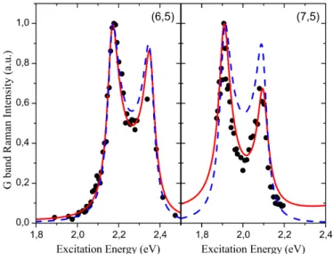
2, (1) where Γ is a resonance window. Γ is a damping constant and is related to the finite lifetime of the intermediate state. In Raman excitation profiles of the G-band, two resonance peaks, which correspond to the incident and scattered resonances, clearly appear with Γ = 26−43 meV30 for chirality-separated SWCNTs.
Fig. 3. G-band resonance energy profile for (6,5) and (7,5) SWCNTs. The black circles are experimental data and the full red line is the present calculation with all matrix elements, while the dashed blue line is the same calculation using constant matrix elements. The electronic gap between the valence and conduction bands was corrected in a few electronvolts to fit with the experimental transitions.31 Figure 3 is taken from Ref. (31) with permission of L. G. Moura, et al.,Phys. Rev. B,89, 035402, 6 January 2014, Copyright by the American Physical Society.
Polarized Raman scattering spectroscopy is performed by using polarized inci- dent and scattered lights, and it provides the information of the phonon symmetry, based on the group theory. The polarization effects of the G-band peaks have been reported.15 In the case of SWCNTs, however, the resonance Raman effect and depolarization effects32 due to the anisotropic geometry of SWCNTs are more prominent than the intrinsic polarization property of Raman scattering.33 As a result, the intensity of the G-band is simply strong when the tube axis is parallel to the polarization of the incident and scattering light. The strong anisotropy is useful for analysis of the tube orientation of SWCNTs.34
Phonon vibration frequency and Raman shift are affected by isotope abundance.
Although the natural abundance of 13C carbon is constant (1.1 %), it is possible to synthesize SWCNTs with arbitrary isotope abundance of carbon by using the
carbon source of 13C.35 Raman shift of12C and13C-SWCNTs is expressed by ω12C(1−x)13Cx =ω12C
√ m12
m12(1−x) +m13x (2) where, ω12Cis the phonon frequency of pure12C-SWCNT, andω12C(1−x)13Cx is the phonon frequency of mixture of12C and13C-SWCNT,xis13C atom concentration, m12andm13are the mass of12C and13C carbon atoms, respectively. Equation (2) is available for G-band, D-band and 2D-band,36 and the isotope abundance can be investigated by Raman scattering spectroscopy, as shown in Fig. 4.
Fig. 4. Raman spectra of SWCNTS containing different amount of13C; RBM peaks, D-band, G-band and 2D-band spectral regions, taken from Ref. (36) with permission of Elsevier.
1.2. D-band
The D-band is a defect-induced peak in graphitic structure and the D-band is explained by double resonance effect.37,38 Therefore, the intensity ratio between the G-band and D-band is often used for the evaluation of crystallinity of graphitic structure for not only SWCNTs but also multi-walled carbon nanotube and other graphitic carbon materials. Tuinstra-Koening relation14
ID/IG =C(λ)/LD, (3) where,IGandIDare the intensity of the G-band and D-band, respectively,C(λ) is the proportionality constant, which depends on the excitation laser wavelength, and LDis the crystallite size, is used for characterization of the crystallinity of graphitic structure. In the case of graphene, LDis estimated to be a few nm.39
While D-band is the defect-induced peak, it corresponds to a phonon aroundK point. Double resonance effect37,38 involving scattering of phonon around Kpoint
and inelastic scattering with defect structure, causes D-band peak. Because of the double resonance effect, Raman shift of the D-band (ωD) shows the excitation light energy dependence (dωD/dEex∼53 cm−1eV−1).38
2D-band is the second-order Raman scattering of D-band phonon and it may be also called G’-band. It also appears due to double resonance effects.37,38 In the case of 2D-band, inelastic scattering with defects is not required and 2D-band is observed from graphitic materials even without defect structure. Because no defect is involved, some people preferred to call as G’-band rather then 2D-band. The shape of the 2D-band of SWCNTs is different from that of double-walled carbon nanotubes (DWCNTs)40 and the 2D-band is a signature for distinction between SWCNTs and DWCNTs.
1.3. RBM peaks
Fig. 5. RBM spectra of SDS-wrapped SWCNTs in solution, measured with 76 different laser lines, taken from Ref. (41) with permission of C. Fantini, et al., Phys. Rev. Lett.,93, 147406, 29 September 2004 Copyright by the American Physical Society. Each sharp peaks correspond to different chirality SWCNTs.
RBM peaks appear in the lower wavenumber region. Raman shift of RBM peaks (ωRBM) is inversely proportional to itsdtube,42,43 as follows,
ωRBM=A/dtube. (4)
Therefore, RBM peaks are often used to analyze the dtube distribution of SWCNT samples. However, as discussed in Sec. 2.1,ωRBMis not exactly expressed by Eq. (4), because of the environmental effects on ωRBM. Considering the environmental ef-
fects, the following equation,
ωRBM=A/dtube+B (5)
is often used. This simple equation is useful for analysis of SWCNT tube diameter, although the values of Aand B vary depending the environments, as discussed in Sec. 2.1.
Fig. 6. RBM Raman intensity per length for SWCNTs with 0.6 < dtube<1.6 nm.(a) and (b) are forE22(
A02)
and freee-hatk22in semiconducting-SWCNTs, respectively. Filled and open circles are for SI and SII tubes. (c) and (d) are forE11L
(A02)
and freee-hatk11Lin metallic SWCNTs, respectively. The intensity in the free el-ph case has been multiplied by 200. The arrows indicate theθdecreasing direction (A, armchair side; Z, zigzag side). In (d), within a family the armchair tube has a larger intensity than its neighbor due to a node effect. Figure 6 is taken from Ref. (44) with permission of J. Jiang, et al.,Phys. Rev. B,75, 035405, 8 January 2007, Copyright by the American Physical Society.
RBM peaks are strongly enhanced by resonance Raman effect and the resonance Raman effect is also expressed by Eq. (1). As shown in Fig. 5, spectra of RBM peaks change with changing the excitation wavelength. Each peaks come from different chirality and the intensity also clearly depend on the chirality. In general, SWC- NTs with smaller chiral angle (near zigzag) exhibit stronger intensity of the RBM peaks,44 as shown in Fig. 6. Additionally, the relationship between the intensity of G+ and RBM peaks is investigated for chirality-separated SWCNT samples and it shows the chirality dependence.20
1.4. Kataura plots
As mentioned above, the intensity of RBM peaks is strongly enhanced by resonance Raman scattering effect. The phonon energy of RBM peaks is approximately a few tens of milli electronvolts. When Eexis in visible or infrared range,Ephonon of RBM peaks is quite small compared withEex. Therefore, it is usually impossible to distinguish the incident and scattered resonances (Eq. (1)) and only Eii is simply regarded as the resonance energy in RBM peaks.
The relationship betweenωRBMandEiiis called Kataura plot.49 Figure 7 shows an example of Kataura plot, which is a compilation of experimental data.41,45–48 Because bothωRBM42,43andEii50 are roughly proportional to 1/dtube, the plots in Fig. 7 appear along lines from the lower left to the top right. Here, theEiiS andEiiM are the i-th optical transition energy of semi-conducting and metallic SWCNTs, respectively. In Fig. 7, five different optical transition energies are shown, such as
1001 150 200 250 300 350 400
1.2 1.4 1.6 1.8 2 2.2 2.4 2.6 2.8 3
(12,1) (11,0)
(9,1) (7,5)
(8,6) (7,6) (11,1)
(8,7) (13,0)
(9,8) (14,1)
(10,0)
(6,5) (6,4)
(10,1) (7,7)
(12,0) (8,8)
(9,9)
(13,1) (15,0) (10,10)
(6,6)
(9,0)
(9,1)
(6,5)
(10,0) (11,0)
(7,5) (8,6)
(7,6)
(8,1) (6,4) (16,1)
Raman Shift (cm
-1)
O p ti c a l T ra n s it io n E n e rg y ( e V )
(8,1)
(9,7)
785 nm 633 nm 488 nm
514.5 nm 532 nm
830 nm (14,0)
(15,1) (17,0) (16,0) (17,1)
(10,8) (10,9)
<ES11>
<ES22>
<EM11>
<ES33>
(14,1) (13,0)
(16,0) (17,1)
(19,0) (20,1) (22,0)
(18,1)
(17,6) (20,0)
(10,6)
(18,1) (19,1) (21,0) (11,11)
(12,12) (13,13)
<ES44>
(8,0)
(8,0)
(5,4) (5,4)
2n+m=19
2n+m=22 2n+m=20 2n+m=21 2n+m=29
Fig. 7. Empirical Kataura plots of SWCNTs. Blue open circles (◦)45 are measured from as- grown SWCNTs. Blue cross marks (×) are calculated from the empirical equation.45 Green open circles (◦),46red open circles (◦)41and filled circle (•)47are measured from dispersed SWCNTs in solution. Green filled circles (•)48 are measured from suspended SWCNTs. The energy of excitation laser, which is widely used for Raman scattering measurement of SWCNTs, is shown.
E11S, E11M, E22S, E33S and ES44. Eii depends on bothdtube and the chiral angle (θ).
Therefore, the plots do not appear just along lines and slightly spread. In Fig. 7, the plots with the same value of (2n+m) are connected with line segments and they show so-called “family pattern”.51 Some of the plots are shown with chiral index (n, m) or the number of (2n+m). Semi-conducting SWCNTs are often categolized into two groups. Semi-conducting SWCNTs with (2n+m) mod 3 = 1 and 2 are called ‘type-I’ (‘SI’ or ‘mod2’) and ‘type-II’ (‘SII’ or ‘mod1’) SWCNTs, respectively.
Some properties of SWCNTs show the type-dependence. For example,Eii depends on strain and whetherEii increases or decreases is determined by the type.52
Based on Kataura plot, it is possible to assign the chirality from measured RBM peaks. When Eii is close to the Eex, the RBM peaks are observed. The resonance window (Γ) depend on SWCNT samples, such as SDS wrapped SWNTs in solution (Γ = 60 meV) and bundled SWCNTs (Γ = 120 meV).41 According to Kataura plots, for example, RBM peaks in Fig. 1 correspond to semiconducting SWCNTs with 2n+m= 29 and metallic SWCNTs with 2n+m= 21.
2. Environmental effects on Kataura plots
The plots of some typical SWCNT samples, such as as-grown SWCNT,45 which may be bundled, surfactant-wrapped SWCNTs in water solution,46and suspended in air,48are shown in Fig. 7. Although these plots are slightly different, they show a similar feature. Note that the blue cross marks are calculated from the empirical equation.45
Additionally, two more kinds of SWCNTs, which are vertically-aligned SWCNTs and suspended SWCNTs in vacuum, are considered and their plots are added in Kataura plot in Fig. 8. These two kinds of SWCNTs are clearly different from former SWCNT samples. ωRBM and Eii considerably change depending on the surrounding condition around SWCNTs, which is called “environmental effects”.
In the following, the environmental effects on ωRBMandEii are discussed.
2.1. Raman shift
dtube is geometrically defined by the chirality index (n, m) with the lattice constant (aC−C) of the honeycomb structure of carbon atoms, as follows
dtube=√ 3aC−C
√n2+nm+m2
π . (6)
aC−C of graphene is 0.142 nm and the value of aC−C = 0.142 nm is also used for SWCNTs.55 Note that the value ofaC−C= 0.144 nm has often been employed for the calculation of SWCNT diameter.56 Density functional theory calculation reveals thataC−Cdepends ondtubein smalldtuberange andaC−Cincreases with decreasing dtube.57 aC−C of SWCNTs with 0.6 nm in diameter is approximately 0.144 nm.
However, typicaldtube of SWCNTs, which are synthesized experimentally, is 0.7 nm at the smallest (for example (6,5) SWCNT). For simple comparison, the coefficients
of the equations, such asAin Eq. (4), orA andB in Eq. (5), are re-calculated by using theaC−C= 0.142 nm instead ofaC−C= 0.144 nm.
ωRBM is simply proportional to 1/dtube,.42,43 With given the speed of sound in SWCNTs, theory predicts that the value of A is 227 cm−1nm.42 In fact, in the case of suspended and isolated SWCNTs in vacuum, the value of A is mea- sured to be 227 cm−1nm54 or 228 cm−1nm.58 Because suspended SWCNTs in vac- uum are perfectly free, they exhibit their intrinsic properties. In isolated and sus- pended SWCNTs, experimental and theoretical results show good agreement of the diameter dependence of ωRBM. The same value of A (227 cm−1nm) is obtained from vertically-aligned SWCNTs.59 Hence, vertically-aligned SWCNTs are directly grown on substrates. They vertically stand up on the substrate with entangling each other, and form the small-bundle structure.60 The value ofA= 227 cm−1nm suggests that partially-suspended and isolated SWCNTs exist in vertically-aligned SWCNT samples and they are not covered with any substances.
Generally, as-grown SWCNTs are bundled or interacting with other materials.
Therefore, in order to express the relationship between ωRBM and dtube, various values ofAhad been reported. A= 244.6 cm−1nm (A= 248 cm−1nm withaC−C= 0.144 nm in the original literature)61was obtained from SWCNTs grown on silicon substrates andA= 223.75 cm−1nm was from bundled SWCNT samples.62
As the other type of approximation to express the environmental effects on ωRBM, Eq. (5) is frequently used. The value of B express the “environmen- tal effect” on ωRBM, and many combination of the values (A, B) is proposed
Fig. 8. Relationship betweenωRBM and theEii(Kataura plot) obtained from suspended SWC- NTs. The PL and Raman scattering measurements were performed in vacuum (open diamond,♢) and water vapor (open circle,◦). The plots of as-grown SWCNTs (×)45and surfactant wrapped SWCNTs in solution (+)46are shown as reference. The open ()45and filled square ()53marks present the Raman resonant energy andωRBM, which are calculated from the empirical equations for as-grown and vertically aligned SWCNT samples, respectively. Figure 8 is taken from Ref.
(54) with permission of S. Chiashi, et al.,Phys. Rev. B,91, 155415, 15 April 2015, Copyright by the American Physical Society.
Fig. 9. Raman scattering spectra (G-band and RBM peak) from (10,5) SWCNT, measured in vacuum (4.0 Pa) and water vapor (630 Pa). The wavelength of the excitation laser is 785 nm.
Figure 9 is taken from Ref. (63) with permission of Y. Homma, et al.,Phys. Rev. Lett.,110, 157402, 9 April 2013, Copyright by the American Physical Society.
for various SWCNT samples. For example, (A, B) = (220.4,12.5) [(223.5,12.5) with aC−C = 0.144 nm in the original literature],64 (218,17) for metallic SWC- NTs and (223,10) for semi-conducting SWCNTs,41 (214.4,18.7),65 (215,18)66 and (217.8,15.7)45 are measured from SDS-wrapped SWCNTs. (A, B) = (204,27)67 is reported for suspended SWCNTs and the value of B is non-zero in spite of sus- pended SWCNTs. The non-zero value of B suggests that the suspended SWCNTs are adsorbed with water layer and the adsorption effects modifiedωRBM,54 as dis- cussed later. Equation (5) is also available for the case of suspended SWCNTs in vacuum with (A, B) = (227,0) or (228,0), and it is practically useful for investiga- tion of RBM peaks and estimation of the tube diameter distribution of SWCNTs, although the available surrounding conditions and diameter range should be con- sidered. Note that A and B are simply fitting parameters and they do not have physical meanings.
In order to investigate the environmental effect onωRBM, some models are pro- posed. One is a model, where SWCNT is surrounded by an environmental shell and it is under inward pressure.59 In this model,
ωRBM= (A/dtube)
√
1 +C ∗dtube2
(7) where
C=6( 1−ν2)
Eh K
s02 (8)
is obtained, where ν is the Poissons ratio, E is the Youngs modulus, h is the thickness of the SWCNT wall, K is the van der Waals interaction strength, and
s0 is is the equilibrium separation between the SWCNT wall and the environment shell. In Eq. (7), the values of (A, C) = (227,0.05786)59 are available for various SWCNT sample. Of course, Eq. (7) with (A, C) = (227,0) is available for suspended SWCNTs in vacuum.59
Other one is a model, where SWCNT is wrapped with surrounding media. As- suming that the surrounding media physically adsorb on the outer surface of SWC- NTs, the interaction between the SWCNT and the media is regarded to be the van der Waals interaction and the mechanical coupling of radial breathing vibration between SWCNT and the surrounding media causes the environmental effect on ωRBM.54 ωRBMin (=A/dtube) is the intrinsic RBM frequency of SWCNT,ωadis the vibration frequency of radial breathing mode of the surrounding media andωexRBMis the extrinsic frequency due to the environmental effects. Based on simple dynamic considerations, the dynamical matrix is
[
(ωad)2+K11 K12
K21
(ωRBMin )2
+K22
]
(9) and the matrix gives ωexRBM as the eigenvalue. Kij is the interaction between SWCNT and the surrounding media and they are calculated by integration of the interaction between the carbon atoms and atoms of the surrounding media.
In this model, the environmental effects of SWCNTs (bundle structure) and wa- ter adsorption layer as the surrounding media can be calculated with the value of A= 227 cm−1nm, and the calculated results show good agreement with the experi- ments for widedtuberange.54 RBM peak from suspended (10,5) SWCNT measured in vacuum and water vapor are shown in Fig. 9. Sharp single RBM peak clearly appears and the peak is up-shifted in water vapor. The up-shift comes from the adsorption of water molecules on the outer surface of SWCNT. Since the interaction between water and SWCNT is not so strong, strain or inward pressure do not occur in suspended SWCNT.
SWCNTs lying on substrates are one of the most typical SWCNT samples. and theirωRBMare affected by contact with substrates. However, the substrate effect on ωRBMis complicate, because the substrate contact is not axial symmetry, the radical deformation may affect68 and the interaction between SWCNTs and substrates is very diverse. By using suspended SWCNTs over the trench structure, the substrate effect is investigated and ωRBM of supported parts, which is in contact with the substrate, is a few cm−1 higher than that of suspended parts.69 Axial strain also affects ωRBMand 10% tensile strain causes up-shift by a few cm−1.70
2.2. Resonance energy
In order to determine the resonance Raman energy, Raman scattering spectra are measured by continuously changing the wavelength of excitation light.41 Usually, laser source is used as the excitation light and the different optical systems for each wavelength are needed. Therefore, it is not so easy to measure the resonance
Fig. 10. Emission and excitation wavelengths of surfactant-wrapped SWCNTs (×), suspended SWNTs in air (◦) and suspended SWCNTs in vacuum (•).71 While no substance adsorb on the suspended SWCNTs in vacuum, water molecules adsorb on the outer surface of suspended SWCNTs in air. Figure 10 is taken from Ref. (71) with permission of Copyright c⃝2008, American Chemical Society.
Raman energy. On the other hand, photoluminescence (PL) spectroscopy is useful tool to measure Eii although PL emission is measured from only semi-conducting SWCNTs. Only by changing the excitation wavelength, PL spectroscopy gives us the information ofEii.64 Additionally, it is reported that Raman excitation profiles of RBM peaks is almost the same as PL emission spectra.72 Here, assuming that the resonance Raman energy of RBM peaks is simply equal toEii which are obtained by PL spectroscopy, the environmental effects of the resonance Raman energy is discussed.
Eii is not simply the energy difference between a pair of van Hove singularity peaks in the electronic density of states of SWCNTs. The interaction between excited electron and hole, and between excited electron and the other electrons should be considered and these interactions determine the binding energy of exciton.
The binding energy of exciton of SWCNTs is relatively large and the binding energy contributes to Eii.73 The binding energy depends on the dielectric constant, ϵ because the Coulomb interaction is a function ofϵ. The dielectric constant is affected by the surrounding condition of SWCNTs and it is the one of the origin of the environmental effects of Eii. Usually, in the case of SWCNTs, Eii decreases with increasing the dielectric constant.73
As mentioned in Sec. 2.1, suspended SWCNTs in vacuum are perfectly free from any substances and they show the intrinsic property of SWCNTs. Their Eii are measured by PL spectroscopy and the value of Eii is larger than those in the other conditions,71as shown in Fig. 10. E11andE22of suspended SWCNTs in vacuum are clearly larger than those of suspended SWCNTs in air, which are adsorbed with water layer, and surfactant-wrapped SWCNTs. The same value of Eii is obtained from vertically-aligned SWCNTs.74 It also suggests the existence of partially suspended and isolated SWCNTs in vertically-aligned SWCNT samples.
The environmental effect on Eii is investigated by the immersion of suspended SWCNTs into various liquids.75 SWCNTs exhibit different Eii depending on the dielectric constant of liquids.
Additionally, the interaction among SWCNTs in bundle structure decreasesEii and increase the resonance Raman window (Γ).41 Γ of SDS-wrapped SWCNTs is 65 meV, while that of bundled SWCNT is 112 meV.41 The similar bundling effects onEii is measured by PL spectroscopy.76
Strain changesEiiand the shift ofEii shows type-dependence.52,77 Small band gap appears in metallic SWCNTs due to strain. Whether Eii of semi-conducting SWCNTs increases or decreases depends on the value ofp= (n−m) mod 3
∆E= sgn (2p+ 1) 3t0[(1 +ν)σcos 3θ+γsin 3θ] (10) where p= 1 or p=−1 is for type-I or type-II, respectively,t0 is the tight-binding overlap integral,ν is the Poisson’s ratio,σandγare uniaxial and torsional strains, respectively.52
2.3. Temperature dependence
Raman scattering spectra depend on temperature. It is well-known that the inten- sity ratio between Stokes and anti-Stokes scattering is a function of temperature, as follows
IAS IS
= exp (
−Ephonon kBT
)
(11) where, ISand IAS are the intensity of Stokes and anti-Stokes scattering,kB is the Boltzmann constant, and T is temperature. It is generally possible to obtain the phonon temperature from the intensity ratio. However, in the case of the G-band of SWCNTs, Eq. (11) is not valid. The G-band intensity is strongly enhanced by resonance Raman effect and the phonon energy of the G-band (approximately 0.2 eV) is relatively large. Therefore, the scattered resonance energy is different between Stokes and anti-Stokes (Eex±Ephonon) and Raman excitation profiles are also different.41
Although Eq. (11) is not available for the G-band, it is possible to measure the SWCNT temperature from Raman shift of the G-band. Generally, with increas- ing temperature, Raman shift decreases and the peak width increases because of nonharmonic component of lattice vibration. Raman shift of the G-band decreases with increasing temperature78 79 and the temperature dependence of the G+ peak is simply expressed by80
ωG+(T) =ω0− a
exp (b~ω0/kBT)−1 (12) whereh(= 2π~) is the Planck constant anda,bandω0are fitting parameters. a= 38.4 cm−1,b= 0.438 andω0= 1594 cm−1 are valid in the wide temperature range (form 0 to 1000 K).80 In Fig. 11, the temperature dependence of ωG+ measured from different SWCNT samples and the curve calculated by Eq. (12) are shown.
In Kataura plot, the temperature dependence is important, because bothωRBM
andEii depend on temperature. RBM peaks exhibit downshift of Raman shift and broadening of peak and Eii also decrease width with increasing temperature.41,81
Fig. 11. Temperature dependence of Raman shifts of G+peaks for various SWNT samples mea- sured with a 488.0 nm excitation laser and for HiPco sample measured with three excitation lasers (488.0, 514.5, and 632.8 nm). The dashed line is a fitting line calculated using Eq. (12). The graph is taken from Ref.80
The temperature dependence of Eii of semi-conducting SWCNTs is investigated by PL spectroscopy,82 and the energy shift of Eii (∆Eii) is expressed by Varshni equation, as follows
∆Eii(T) =− αT2
T+β (13)
where, αandβ are the constants. Whileα= 0.075 meV/K andβ = 600 K are ob- tained in the case ofE11of suspended (12,2) SWCNT in lower temperature range,82 α = 0.177 meV/K and β = 1800 K are measured from suspended SWCNTs with various chiralities in the higher temperature range.83 The temperature dependence of ωRBM is also reported. The obtained values of ∂ωRBM/∂T are diverse, such as ∂ωRBM/∂T = −0.013 and −0.015 cm−1/K,84 −0.0045 and −0.009 cm−1/K,78
∼0.006 cm−1,79 and−0.001 ∼ −0.015 cm−1/K.80
Temperature increase often occurs during Raman scattering measurement. The optical absorption cross-section of SWCNTs is a few 10×1018cm2/atom at theEii (on-resonance).85 The temperature of SWCNTs under light irradiation is deter- mined by the power density of excitation light, the light absorption cross-section, the thermal conductivity and the thermal conductance between SWCNTs and the surrounding system. Especially, the temperature of SWCNTs is easily increased in the cases of SWCNTs in vacuum, on substrates with low thermal conductivity and
suspended SWCNTs. During the measurement in atmospheric ambient, it is pos- sible that SWCNTs under light irradiation are damaged or burned by oxidization.
Even without damage, the temperature dependence of Eii andωRBMcould appear in RBM spectra.
3. Acknowledgments
This work is supported by JSPS KAKENHI Grant numbers JP15H05760, JP16H02079 and JP18H05329, Japan and by JST CREST Grant Number JP- MJCR17I3, Japan. We would like to thank Ms. Pengyingkai Wang at UTokyo for her technical help in manuscript preparation.
References
1. S. Iijima and T. Ichihashi, Single-shell carbon nanotubes of 1-nm diameter, Nature.
363, 603–605, (1993).
2. D. S. Bethune, C. H. Kiang, M. S. de Vries, G. Gorman, R. Savoy, J. Vazquez, and R. Beyers, Cobalt-catalysed growth of carbon nanotubes with single-atomic-layer walls,Nature.363, 605–607, (1993).
3. A. M. Rao, E. R. S. Bandow, B. C. P. C. Eklund, K. A. Williams, S. Fang, K. R. Sub- baswamy, M. Menon, A. Thess, R. E. Smalley, G. Dresselhaus, and M. S. Dresselhaus, Diameter-selective Raman scattering from vibrational modes in carbon nanotubes, Science.275, 187–191, (1997).
4. A. Thess, R. Lee, P. Nikolaev, H. J. Dai, P. Petit, J. Robert, C. H. Xu, Y. H. Lee, S. G. Kim, A. G. Rinzler, D. T. Colbert, G. E. Scuseria, D. Tomanek, J. E. Fischer, and R. E. Smalley, Crystalline ropes of metallic carbon nanotubes, Science. 273, 483–487, (1996).
5. H. Dai, A. G. Rinzler, P. N. Nikolaev, A. Thess, D. T. Colbert, and R. E. Smal- ley, Single-wall nanotubes produced by metal-catalyzed disproportionation of carbon monoxide,Chem. Phys. Lett.260, 471–475, (1996).
6. J. Kong, H. T. Soh, A. M. Cassell, C. F. Quate, and H. J. Dai, Synthesis of individual single-walled carbon nanotubes on patterned silicon wafers, Nature. 395, 878–881, (1998).
7. Y. Murakami, S. Chiashi, Y. Miyauchi, M. H. Hu, M. Ogura, T. Okubo, and S. Maruyama, Growth of vertically aligned single-walled carbon nanotube films on quartz substrates and their optical anisotropy, Chem. Phys. Lett. 385, 298–303, (2004).
8. K. Hata, D. N. Futaba, K. Mizuno, T. Namai, M. Yumura, and S. Iijima, Water- assisted highly efficient synthesis of impurity-free single-walled carbon nanotubes, Science.306, 1362–1364, (2004).
9. A. Ismach, L. Segev, E. Wachtel, and E. Joselevich, Atomic-step-templated formation of single wall carbon nanotube patterns,Angew. Chem. Int. Ed.43, 6140–6143, (2004).
10. A. M. Cassell, N. R. Franklin, T. W. Tombler, E. M. Chan, J. Han, and H. J. Dai, Directed growth of free-standingsingle-walled carbon nanotubes, J. Am. Chem. Soc.
121, 7975–7976, (1999).
11. M. S. Arnold, A. A. Green, J. F. Hulvat, S. I. Stupp, and M. C. Hersam, Sorting carbon nanotubes by electronic structure using density differentiation,Nat. Nanotechnol.1, 60–65, (2006).
12. X. Tu, S. Manohar, A. Jagota, and M. Zheng, DNA sequence motifs for structure- specific recognition and separation of carbon nanotubes,Nature.460, 250–253, (2009).
13. S. Maruyama, R. Kojima, Y. Miyauchi, S. Chiashi, and M. Kohno, Low-temperature synthesis of high-purity single-walled carbon nanotubes from alcohol, Chem. Phys.
Lett.360, 229–234, (2002).
14. F. Tuinstra and J. L. Koenig, Raman spectrum of graphite, J. Chem. Phys. 53, 1126–1130, (1970).
15. A. Jorio, M. A. Pimenta, A. G. Souza, G. G. Samsonidze, A. K. Swan, M. S. Unlu, B. B. Goldberg, R. Saito, G. Dresselhaus, and M. S. Dresselhaus, Resonance Raman spectra of carbon nanotubes by cross-polarized light,Phys. Rev. Lett.90, 107403–1–
107403–4, (2003).
16. S. Lebedkin, F. Hennrich, T. Skipa, and M. M. Kappes, Near-infrared photolumines- cence of single-walled carbon nanotubes prepared by the laser vaporization method, J. Phys. Chem. B.107, 1949–1956, (2003).
17. Y. Kobayashi, T. Yamashita, Y. Ueno, O. Niwa, Y. Homma, and T. Ogino, Extremely intense Raman signals from single-walled carbon nanotubes suspended between Si nanopillars,Chem. Phys. Lett.386, 153–157, (2004).
18. H. B. Son, Y. Hori, S. G. Chou, D. Nezich, G. G. Samsonidze, G. Dresselhaus, M. S.
Dresselhaus, and E. B. Barros, Environment effects on the Raman spectra of individual single-wall carbon nanotubes: Suspended and grown on polycrystalline silicon,Appl.
Phys. Lett.85, 4744–4746, (2004).
19. V. Avramenko and S. B. Rochal, Symmetry of the carbon nanotube modes and their origin from the phonon branches of graphene,Phys. Rev. B.87, 035407–1–035407–8, (2013).
20. Y. Piao, J. R. Simpson, J. K. Streit, G. Ao, M. Zheng, J. A. Fagan, and A. R. H.
Walker, Intensity ratio of resonant Raman modes for (n,m) enriched semiconducting carbon nanotubes,ACS Nano.10, 5252–5259, (2016).
21. X. Blase, L. X. Benedict, E. L. Shirley, and S. G. Louie, Hybridization effects and metallicity in small radius carbon nanotubes,Phys. Rev. Lett.72, 1878–1881, (1994).
22. A. Jorio, A. G. Souza, G. Dresselhaus, M. S. Dresselhaus, A. K. Swan, M. S. Unlu, B. B. Goldberg, M. A. Pimenta, J. H. Hafner, C. M. Lieber, and R. Saito, G-band resonant Raman study of 62 isolated single-wall carbon nanotubes,Phys. Rev. B.65, 155412–1–155412–9, (2002).
23. H. Telg, J. G. Duque, M. Staiger, X. Tu, F. Hennrich, M. M. Kappes, M. Zheng, J. Maultzsch, C. Thomsen, and S. K. Doorn, Chiral index dependence of the G+ and G−Raman modes in semiconducting carbon nanotubes,ACS Nano.6, 904–911, (2012).
24. B. Hatting, S. Heeg, K. Ataka, J. Heberle, F. Hennrich, M. M. Kappes, R. Krupke, and S. Reich, Fermi energy shift in deposited metallic nanotubes: A Raman scattering study,Phys. Rev. B.87, 165442–1–165422–5, (2013).
25. H. Farhat, H. Son, G. Samsonidze, S. Reich, M. Dresselhaus, and J. Kong, Phonon softening in individual metallic carbon nanotubes due to the Kohn anomaly, Phys.
Rev. Lett.99, 145506–1–145506–4, (2007).
26. S. D. M. Brown, A. Jorio, P. Corio, M. S. Dresselhaus, G. Dresselhaus, R. Saito, and K. Kneipp, Origin of the Breit-Wigner-Fano lineshape of the tangential G-band feature of metallic carbon nanotubes,Phys. Rev. B.63, 155414–1–155414–8, (2001).
27. J. S. Park, K. Sasaki, R. Saito, W. Izumida, M. Kalbac, H. Farhat, G. Dresselhaus, and M. S. Dresselhaus, Fermi energy dependence of the G-band resonance Raman spectra of single-wall carbon nanotubes,Phys. Rev. B.80, 081402(R)–1–081402(R)–4, (2009).
28. K. Nguyen, A. Gaur, and M. Shim, Fano lineshape and phonon softening in single
isolated metallic carbon nanotubes,Phys. Rev. Lett.98, 145504–1–145504–4, (2007).
29. M. A. Pimenta, A. Marucci, S. A. Empedocles, M. G. Bawendi, E. B. Hanlon, A. M.
Rao, P. C. Eklund, R. E. Smalley, G. Dresselhaus, and M. S. Dresselhaus, Raman modes of metallic carbon nanotubes,Phys. Rev. B.58, R16016–R16019, (1998).
30. J. G. Duque, H. Chen, A. K. Swan, A. P. Shreve, S. Kilina, S. Tretiak, X. Tu, M. Zheng, and S. K. Doorn, Violation of the condon approximation in semiconducting carbon nanotubes,ACS Nano.5, 5233–5241, (2011).
31. L. G. Moura, M. V. O. Moutinho, P. Venezuela, C. Fantini, A. Righi, M. S. Strano, and M. A. Pimenta, Raman excitation profile of the G band in single-chirality carbon nanotubes,Phys. Rev. B.89, 035402–1–035402–5, (2014).
32. H. Ajiki and T. Ando, Aharonov-Bohm effect in carbon nanotubes,Physica B.201, 349–352, (1994).
33. G. S. Duesberg, I. Loa, M. Burghard, K. Syassen, and S.Roth, Polarized Raman spectroscopy on isolated single-wall carbon nanotubes, Phys. Rev. Lett. 85, 5436–
5439, (2000).
34. H. H. Gommans, J. W. Alldredge, H. Tashiro, J. Park, J. Magnuson, and A. G. Rinzler, Fibers of aligned single-walled carbon nanotubes: Polarized Raman spectroscopy,J.
Appl. Phys.88, 2509–2514, (2000).
35. L. Liu and S. Fan, Isotope labeling of carbon nanotubes and formation of 12C-13C nanotube junctions,J. Am. Chem. Soc.123, 11502–11503, (2001).
36. S. D. Costa, C. Fantini, A. Righi, A. Bachmatiuk, M. H. Rummeli, R. Saito, and M. A. Pimenta, Resonant Raman spectroscopy on enriched 13c carbon nanotubes, Carbon.49, 4719–4723, (2011).
37. L. G. Can¸cado, M. A. Pimenta, R. Saito, A. Jorio, L. O. Ladeira, A. Grueneis, A. G.
Souza, G. Dresselhaus, and M. S. Dresselhaus, Stokes and anti-Stokes double reso- nance Raman scattering in two-dimensional graphite, Phys. Rev. B.66, 035415–1–
035415–5, (2002).
38. R. Saito, A. Jorio, A. G. Souza, G. Dresselhaus, M. S. Dresselhaus, and M. A. Pi- menta, Probing phonon dispersion relations of graphite by double resonance Raman scattering,Phys. Rev. Lett.88, 027401–1–027401–4, (2002).
39. M. Lucchese, F. Stavale, E. M. Ferreira, C. Vilani, M. Moutinho, R. B. Capaz, C. Achete, and A. Jorio, Quantifying ion-induced defects and Raman relaxation length in graphene,Carbon.48, 1592–1597, (2010).
40. R. Pfeiffer, H. Kuzmany, F. Simon, S. N. Bokova, and E. Obraztsova, Resonance Raman scattering from phonon overtones in double-wall carbon nanotubes, Phys.
Rev. B.71, 155409–1–15540–8, (2005).
41. C. Fantini, A. Jorio, M. Souza, M. S. Strano, M. S. Dresselhaus, and M. A. Pi- menta, Optical transition energies for carbon nanotubes from resonant Raman spec- troscopy: Environment and temperature effects, Phys. Rev. Lett. 93, 147406–1–
147406–4, (2004).
42. G. D. Mahan, Oscillationsions of a thin hollow cylinder: Carbon nanotubes, Phys.
Rev. B.65, 235402–1–235402–7, (2002).
43. V. Perebeinos and J. Tersoff, Valence force model for phonons in graphene and carbon nanotubes,Phys. Rev. B.79, 241409–1–241409–4, (2009).
44. J. Jiang, R. Saito, K. Sato, J. S. Park, G. G. Samsonidze, A. Jorio, G. Dresselhaus, and M. S. Dresselhaus, Exciton-photon, exciton-phonon matrix elements, and resonant Raman intensity of single-wall carbon nanotubes,Phys. Rev. B.75, 035405–1–035405–
10, (2007).
45. P. T. Araujo, S. K. Doorn, S. Kilina, S. Tretiak, E. Einarsson, S. Maruyama, H. Chacham, M. A. Pimenta, and A. Jorio, Third and fourth optical transitions in
semiconducting carbon nanotubes,Phys. Rev. Lett.98, 067401–1–067401–4, (2007).
46. H. Telg, J. Maultzsch, S. Reich, F. Hennrich, and C. Thomsen, Raman intensities of the first optical transitions in carbon nanotubes,phys. stat. sol. (b).243, 3181–3185, (2006).
47. A. Jorio, C. Fantini, M. Pimenta, R. Capaz, G. Samsonidze, G. Dresselhaus, M. Dres- selhaus, J. Jiang, N. Kobayashi, A. Gruneis, and R. Saito, Resonance Raman spec- troscopy (n,m)-dependent effects in small-diameter single-wall carbon nanotubes, Phys. Rev. B.71, 075401–1–075401–11, (2005).
48. T. Michel, M. Paillet, J. Meyer, V. Popov, L. Henrard, P. Poncharal, A. Zahab, and J. Sauvajol, Raman spectroscopy of (n,m)-identified individual single-walled carbon nanotubes,Phys. Status Solidi B.244, 3986–3991, (2007).
49. H. Kataura, Y. Kumazawa, Y. Maniwa, I. Umezu, S. Suzuki, Y. Ohtsuka, and Y. Achiba, Optical properties of single-wall carbon nanotubes, Synth. Met. 103, 2555–2558, (1999).
50. J. C. Charlier and P. Lambin, Electronic structure of carbon nanotubes with chiral symmetry,Phys. Rev. B.57, R15037–R15039, (1998).
51. G. G. Samsonidze, R. Saito, N. Kobayashi, A. Gruneis, J. Jiang, A. Jorio, S. G.
Chou, G. Dresselhaus, and M. S. Dresselhaus, Family behavior of the optical transition energies in single-wall carbon nanotubes of smaller diameters,Appl. Phys. Lett.85, 5703–5705, (2004).
52. L. Yang and J. Han, Electronic structure of deformed carbon nanotubes, Phys. Rev.
Lett.85, 154–157, (2000).
53. P. T. Araujo and A. Jorio, The role of environmental effects on the optical transition energies and radial breathing mode frequency of single wall carbon nanotubes,phys.
stat. sol. (b).245, 2201–2204, (2008).
54. S. Chiashi, K. Kono, D. Matsumoto, J. Shitaba, N. Homma, A. Beniya, T. Yamamoto, and Y. Homma, Adsorption effects on radial breathing mode of single-walled carbon nanotubes,Phys. Rev. B.91, 155415–1–155415–5, (2015).
55. R. Saito, M. Fujita, G. Dresselhaus, and M. S. Dresselhaus, Electronic structure of chiral graphene tubules,Appl. Phys. Lett.60, 2204–2206, (1992).
56. R. Saito, T. Takeya, T. Kimura, G. Dresselhaus, and M. S. Dresselhaus, Raman intensity of single-wall carbon nanotubes,Phys. Rev. B.57, 4145–4153, (1998).
57. K. Kato and S. Saito, Geometries, electronic structures and energetics of small- diameter single-walled carbon nanotubes, Physica E: Low-dimensional Systems and Nanostructures.43, 669–672, (2011).
58. K. Liu, W. Wang, M. Wu, F. Xiao, X. Hong, S. Aloni, X. Bai, E. Wang, and F. Wang, Intrinsic radial breathing oscillation in suspended single-walled carbon nanotubes, Phys. Rev. B.83, 113404–1–113404–4, (2011).
59. P. T. Araujo, I. O. Maciel, P. B. C. Pesce, M. A. Pimenta, S. K. Doorn, H. Qian, A. Hartschuh, M. Steiner, L. Grigorian, K. Hata, and A. Jorio, Nature of the constant factor in the relation between radial breathing mode frequency and tube diameter for single-wall carbon nanotubes,Phys. Rev. B.77, 241403(R)–1–241403(R)–4, (2008).
60. E. Einarsson, H. Shiozawa, C. Kramberger, M. H. Rummeli, A. Gruneis, T. Pichler, and S. Maruyama, Revealing the small-bundle interal structure of vertically aligned single-walled carbon nanotube films,J. Phys. Chem. C.111, 17861–17864, (2007).
61. A. Jorio, R. Saito, J. H. Hafner, C. M. Lieber, M. Hunter, T. McClure, G. Dresselhaus, and M. S. Dresselhaus, Structural (n,m) determination of isolated single-wall carbon nanotubes by resonant Raman scattering,Phys. Rev. Lett.86, 1118–1121, (2001).
62. S. Bandow, S. Asaka, Y. Saito, A. M. Rao, L. Grigorian, E. Richter, and P. C. Eklund, Effect of the growth temperature on the diameter distribution and chirality of single-
wall carbon nanotubes,Phys. Rev. Lett.80, 3779–3782, (1998).
63. Y. Homma, S. Chiashi, T. Yamamoto, K. Kono, D. Matsumoto, J. Shitaba, and S. Sato, Photoluminescence measurements and molecular dynamics simulations of water adsorption on the hydrophobic surface of a carbon nanotube in water vapor, Phys. Rev. Lett.110, 157402–1–157402–4, (2013).
64. S. M. Bachilo, M. B. Strano, C. Kittrell, R. H. Hauge, R. E. Smalley, and R. B. Weis- man, Structure-assigned optical spectra of single-walled carbon nanotubes, Science.
298, 2361–2366, (2002).
65. H. Telg, J. Maultzsch, S. Reich, F. Hennrich, and C. Thomsen, Chirality distribution and transition energies of carbon nanotubes,Phys. Rev. Lett.93, 177401–1–177401–4, (2004).
66. J. Maultzsch, H. Telg, S. Reich, and C. Thomsen, Radial breathing mode of single- walled carbon nanotubes: Optical transition energies and chiral-index assignment, Phys. Rev. B.72, 205438–1–205438–16, (2005).
67. M. Paillet, T. Michel, J. C. Meyer, V. N. Popov, L. Henrard, S. Roth, and J. L.
Sauvajol, Raman active phonons of identified semiconducting single-walled carbon nanotubes,Phys. Rev. Lett.96, 257401–1–257401–4, (2006).
68. J. Soares, A. P. M. Barboza, P. T. Araujo, N. M. B. Neto, D. Nakabayashi, N. Shadmi, T. S. Yarden, A. Ismach, N. Geblinger, E. Joselevich, C. Vilani, L. G. Can¸cado, L. Novotny, G. Dresselhaus, M. S. Dresselhaus, B. R. A. Neves, M. S. C. Mazzoni, and A. Jorio, Modulating the electronic properties along carbon nanotubes via tube- substrate interaction,Nano Lett.10, 5043–5048, (2010).
69. Y. Y. Zhang, H. Son, J. Zhang, M. S. Dresselhaus, J. Kong, and Z. F. Liu, Raman spectra variation of partially suspended individual single-walled carbon nanotubes,J.
Phys. Chem. C.111, 1983–1987, (2007).
70. R. Kumar, M. Aykol, and S. B. Cronin, Effect of nanotube-nanotube coupling on the radial breathing mode of carbon nanotubes, Phys. Rev. B. 78, 165428–1–165428–4, (2008).
71. S. Chiashi, S. Watanabe, T. Hanashima, and Y. Homma, Influence of gas adsorption on optical transition energies of single-walled carbon nanotubes,Nano Lett.8, 3097–
3101, (2008).
72. A. P. Shreve, E. H. Haroz, S. M. Bachilo, R. B. Weisman, S. Tretiak, S. Kilina, and S. K. Doorn, Determination of exciton-phonon coupling elements in single-walled carbon nanotubes by Raman overtone analysis,Phys. Rev. Lett.98, 037405–1–037405–
4, (2007).
73. T. Ando, Excitons in carbon nanotubes, J. Phys. Soc. Jpn.66, 1066–1073, (1997).
74. O. Kiowski, S. Lebedkin, F. Hennrich, S. Malik, H. Rosner, K. Arnold, C. Surgers, and M. M. Kappes, Photoluminescence microscopy of carbon nanotubes grown by chem- ical vapor deposition: Influence of external dielectric screening on optical transition energies,Phys. Rev. B.75, 075421–1–075421–7, (2007).
75. Y. Ohno, S. Iwasaki, Y. Murakami, S. Kishimoto, S. Maruyama, and T. Mizutani, Chirality-dependent environmental effects in photoluminescence of single-walled car- bon nanotubes,Phys. Rev. B.73, 235427–1–235427–5, (2006).
76. J. Lefebvre and P. Finnie, Photoluminescence and f¨orster resonance energy transfer in elemental bundles of single-walled carbon nanotubes, J. Phys. Chem. C. 113, 7536–7540, (2009).
77. K. Arnold, S. Lebedkin, O. Kiowski, F. Hennrich, and M. M. Kappes, Matrix-imposed stress-induced shifts in the photoluminescence of single-walled carbon nanotubes at low temperatures,Nano Lett.4, 2349–2354, (2004).
78. N. R. Raravikar, P. Keblinski, A. M. Rao, M. S. Dresselhaus, L. S. Schadler, and
P. M. Ajayan, Temperature dependence of radial breathing mode Raman frequency of single-walled carbon nanotubes,Phys. Rev. B.66, 235424–1–235424–9, (2002).
79. Z. P. Zhou, L. Ci, L. Song, X. Q. Yan, D. F. Liu, H. J. Yuan, Y. Gao, J. X. W. andL.
F. Liu, W. Y. Zhou, S. S. Xie, Y. X. Du, and Y. J. Mo, The intrinsic temperature effect of Raman spectra of double-walled carbon nanotubes,Chem. Phys. Lett.396, 372–376, (2004).
80. S. Chiashi, Y. Murakami, Y. Miyauchi, and S. Maruyama, Temperature dependence of Raman scattering from single-walled carbon nanotubes: Undefined radial breathing mode peaks at high temperatures,Jpn. J. Appl. Phys.47, 2010–2015, (2008).
81. S. B. Cronin, Y. Yin, A. Walsh, R. B. Capaz, A. Stolyarov, P. Tangney, M. L. Cohen, S. G. Louie, A. K. Swan, M. S. Unlu, B. B. Goldberg, and M. Tinkham, Temper- ature dependence of the optical transition energies of carbon nanotubes: The role of electron-phonon coupling and thermal expansion, Phys. Rev. Lett.96, 127403–1–
127403–4, (2006).
82. J. Lefebvre, P. Finnie, and Y. Homma, Temperature-dependent photoluminescence from single-walled carbon nanotubes,Phys. Rev. B.70, 045419–1–045419–8, (2004).
83. K. Yoshino, T. Kato, Y. Saito, J. Shitaba, T. Hanashima, K. Nagano, S. Chiashi, and Y. Homma, Temperature distribution and thermal conductivity measurements of chirality-assigned single-walled carbon nanotubes by photoluminescence imaging spectroscopy,ACS Omega.3, 4352–4356, (2018).
84. H. D. Li, K. T. Yue, Z. L. Lian, Y. Zhan, L. X. Zhou, S. L. Zhang, Z. J. Shi, Z. N. Gu, B. B. Liu, R. S. Yang, H. B. Yang, G. T. Zou, Y. Zhang, and S. Iijima, Temperature dependence of the Raman spectra of single-wall carbon nanotubes,Appl. Phys. Lett.
76, 2053–2055, (2000).
85. K. Liu, X. Hong, S. Choi, C. Jin, R. Capaz, J. Kim, W. Wang, X. Bai, S. G. Louie, E. Wang, and F. Wang, Systematic determination of absolute absorption cross-section of individual carbon nanotubes,Proc. Natl. Acad. Sci. U.S.A.111, 7564–7569, (2014).