博 士 論 文
Double resonance Raman spectroscopy of
single wall carbon nanotubes and graphene
(単層カーボンナノチューブとグラフェンの
二重共鳴ラマン分光)
朴 珍 成
Acknowledgment
I would like to use this opportunity to thank the many people who contributed to this thesis over the three years of my PhD course studies at Tohoku University. First of all, I am very thankful to my supervisor Professor Riichiro Saito for his teaching me the fundamentals of research. His detail advices not only for physics but also for writing a paper and making a presentation have improved me as a scientist during the three years. I am indebted to Mr. Kentaro Sato who helped me for installing many useful computer programs. I appreciate Dr. Wataru Izumida and Dr. Kenichi Sasaki for stimulating discussion. I would like to thank our collaborator Professor Mildred S. Dresselhaus for her kind advices for nanotube physics. I thank to Professor Young Hee Lee and Mr. Ki Kang Kim for their hospitality and stimulating discussion about the metallicity dependence of the G0 band Raman intensity during my visit to SKKU in Korea. I also thank to Mr. Alfonso Reina and Professor Jing Kong from MIT in USA for stimulating discussion of the G0 band for multi-layer graphene. I am also grateful to Professor Ado Jorio and Dr. Cristiano Fantini for stimulating discussion on their experimental result for resonance window of carbon nanotubes. I also thank to Dr. Jie Jiang and Dr. Eduardo B. Barros for stimulating discussion during their stay in Japan. I am indebted to Monbukagakusho for financing my stay in Japan. Part of the work is supported by the 21st century COE program.
I am sincerely thankful to my Japanese host-family Hiroyuki Toyohara-san and his family for very warm friendship during the three years in Sendai. I am also sincerely thankful to my hometown seniors Professor Young Su Yoon and Dr. Kye Hoon Do who gave me great encouragement to finish this thesis.
Last of all, I appreciate my family for their continuous support.
Abstract
Resonance Raman spectroscopy of single wall carbon nanotubes (SWNTs) is widely used for evaluating the sample quality and the population of (n, m) SWNTs for a given sample, in which a SWNT is specified by two integers n, m. For Raman intensity calculation, we need to understand the electron-photon and electron-phonon interactions, and the Raman resonance window (hereafter, γ) in carbon nanotube system. Here, the γ value is defined by an energy region which gives resonance Raman enhancement. So far, we have used a constant value (0.06 eV) for the γ values for different (n, m) SWNTs. Experimentally, the γ value depends on the tube diameter and chirality. In this thesis, we calculate the Raman resonance window for different (n, m) SWNTs. For a resonance system, the Ra-man resonance window is related to the energy dissipation by inelastic electron-phonon scattering and obtained by calculating the transition probability of a photo-excited elec-tron in the conduction band. The transition probability calculated by elecelec-tron-phonon scattering is given by the Fermi Golden rule. The electron-phonon scattering is considered for 48 possible scattering processes, that is, intra- and inter-valley, forward and backward, emission and absorption, and six phonon modes. The calculated γ values are compared with Raman spectral width in the experiment directly. Using these γ values, we calcu-late the G0 band Raman spectra, especially for a double resonance Raman scattering, which has a strong metallicity dependence in experiment. We suggest that the G0 band comes from the overtone of iTO phonon mode by deducing the G0 band properties. The electron-phonon matrix elements for iTO phonon mode show the dependence of electronic transition energy such as ES
22, E11M, and E33S. The γ values for m-SWNTs give a smaller
value than that for s-SWNTs. This is the reason why the G0 band intensity depends on the metallicity in SWNTs. In addition, we calculate the G0 band spectra of multi-layer graphene, in which the G0 band Raman spectra change in shape, width, and peak position when the number of graphene layers increase from one (1L) to three (3L). Comparison
electrons on the different layers, and then the energy band structure of the multi-layer graphene is split to several energy sub-bands around the Fermi level. The split sub-bands make many double resonance Raman scattering (DR) processes, and give broad the G0 band compared with single layer graphene. Thus, for double (2L) and triple (3L) layer graphenes, there are four and nine possible DR processes for the G0 band, respectively. However, Raman intensity calculation shows that each sub-band which appears due to corresponding DR process depends on its wave vector, and then the G0 band of double and triple layer graphenes have three and five components, respectively. The calculated
G0 band intensity of multi-layer graphene depends on the number of graphene layers, and compares with the experiments.
Contents
1 Introduction 1
1.1 Purpose of this study . . . 1
1.1.1 Raman resonance window . . . 2
1.1.2 Metallicity dependence in G0 band of SWNT . . . 4
1.1.3 G0 band of multi-layer graphene . . . 5
1.2 Organization . . . 6
1.3 Background . . . 8
1.3.1 Synthesis of SWNTs . . . 8
1.3.2 Experimental Raman spectra of SWNT . . . 9
1.3.3 Photoluminescence spectroscopy . . . 10
1.4 Experimental background for this study . . . 11
1.4.1 Resonance Raman window measurement . . . 11
1.4.2 G0 band measurement of SWNT . . . 13
1.4.3 G0 band measurement of multi-layer graphene . . . 15
2 Geometry and electronic structure of SWNT 17 2.1 Geometry of SWNT . . . 17
2.1.1 Graphene is 2D . . . 18
2.1.2 1D unit cell . . . 19
2.1.3 Cutting line . . . 22
2.2 Electronic structure . . . 24
2.2.1 Electronic structure of graphene . . . 24
2.2.2 Electronic structure of SWNT . . . 32
2.2.3 Electronic density of states of SWNT . . . 38 7
3 Calculation method 45
3.1 Electron-photon interaction . . . 45
3.2 Electron-phonon interaction . . . 47
3.3 Raman resonance window . . . 49
3.3.1 Electron-phonon transition probability . . . 49
3.4 Double resonance Raman scattering . . . 50
3.4.1 G0 band of SWNT . . . 51
3.4.2 G0 band of graphene . . . 53
4 Raman resonance window 59 4.1 Electron-phonon scattering processes . . . 59
4.1.1 Semiconducting SWNTs . . . 60
4.1.2 Metallic SWNTs . . . 72
4.2 Calculated result of resonance windows . . . 75
4.3 Summary . . . 78
5 G0 band Raman spectra of SWNT 81 5.1 Origin of G0 band . . . 81
5.2 Important factors of G0 band . . . 83
5.3 G0 band Raman intensity . . . 90
5.4 Summary . . . 93
6 G0 band of multi-layer graphene 95 6.1 Raman scattering processes . . . 95
6.2 G0 band spectra . . . 100
6.2.1 Single layer graphene . . . 100
6.2.2 Double layer graphene . . . 101
6.2.3 triple layer graphene . . . 104
6.3 Summary . . . 107
7 Conclusion 109
Bibliography 111
Chapter 1
Introduction
1.1
Purpose of this study
The physics of carbon nanotubes has rapidly developed into a new research field since multi-wall carbon nanotube was discovered by S. Iijima in 1991 [1] and since single wall carbon nanotubes (SWNTs) was discovered two years later [2, 3]. Carbon nanotube is defined by a cylindrical graphene sheet with a nanoscale (1 nm=10−9 m) diameter and a microscale (1 µm=10−6 m) length. Most of the observed SWNTs have diameter less than 3 nm. Therefore, the SWNTs can be considered as one dimensional (1D) nano-structures because of high aspect ratio. A 1D SWNT can behave as either metallic or semiconducting nanotube depending on two integers (n, m) or two key structural parameters, chirality and diameter [4, 5]. Carbon nanotube is an ideal system for studying the physics of 1D material. Many theoretical and experimental researchers have focused on the relationship between the atomic and electronic structures, or on the electron and electron-phonon interaction. Theoretical and experimental studies in various fields of SWNTs, such as mechanics, optics, chemistry, biology, and electronics, have also focused on both the fundamental physical properties and the commercial application of carbon nanotubes. These studies, in recent years, have generated significant breakthrough in the area of nano-science and technology.
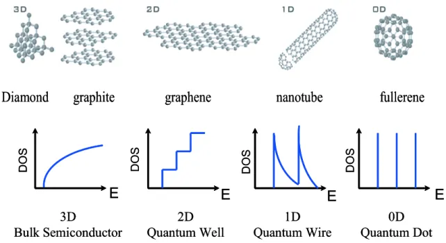
Resonance Raman spectroscopy (RRS) and photoluminescence (PL) spectroscopy pro-vide powerful tools to investigate the geometry and characterization of SWNTs for dif-ferent samples. The unique optical and spectroscopic properties observed in SWNTs are
mainly due to the 1D confinement of the electronic and phonon states. In particular, the 1D confinement of the electron (phonon) state results in the so-called van Hove sin-gularities (vHSs) in the density of states (DOS) of SWNT as a function of energy [5, 6]. The vHSs in the DOS or corresponding the electronic joint density of states (JDOS) play an important role on various optical phenomena. When the incident excitation laser en-ergy matches to the vHS for a SWNT in the JDOS between the valence and conduction bands, one can find a RRS resonance enhancement for the corresponding Raman scat-tering process, which we call resonance Raman spectroscopy. Thus, the RRS intensity allows one to obtain the information in detail about the phonon properties of SWNTs as well as the electronic properties. Recently, many theoretical studies in the optical properties of SWNTs have been performed in order to explain experimental observation. The resonance Raman scattering process in SWNT consists of the electron-photon and electron-phonon scattering processes [7, 8]. Therefore, for the RRS intensity calculation, we need to understand the electron-photon and electron-phonon interaction in a SWNT. The calculation of these interaction matrices has been able to explain the electronic and phonon structure of SWNTs with different chirality and diameter. However, for more precise RRS intensity calculation, we need to understand the Raman resonance window for different SWNTs. Here, the resonance window is defined by an energy region which gives resonance Raman enhancement [9]. In this thesis, we calculate the Raman resonance window for SWNTs with different chirality and diameter. Using these values, we then calculate the Raman spectra especially for a so-called G0 band (∼ 2700 cm−1) of SWNT and multi-layer graphene.
1.1.1
Raman resonance window
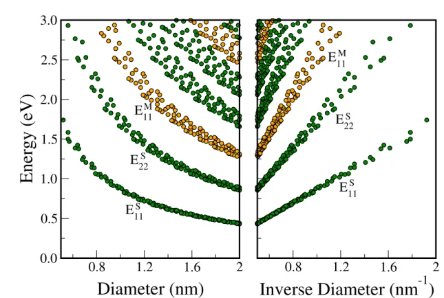
Hereafter we overview the problems that are discussed in this thesis. Detailed definitions will be given in the following chapters. RRS can be used to assign the (n, m) value of a SWNT from a plot of the energy separation Eii between the i-th vHS in the valence
band and the i-th vHS conduction band as a function of diameter of the SWNT, which we call the Kataura plot [10]. RRS of SWNTs is also widely used for evaluating the sample quality and the population [7, 11] of (n, m) SWNTs in actual samples. In the analysis of Raman spectra, not only the resonance energies for the given (n, m) SWNTs, but also the Raman intensities relative to the intensity of other (n, m) SWNTs or of other phonon
modes are important for evaluating the population of SWNTs in the generally available sample in which many (n, m) SWNTs are mixed to one another. The radial breathing mode (RBM, 100∼300 cm−1) and G band (1550∼1600 cm−1) Raman intensities [8,12] and the PL intensity [13] show the presence of a strong (n, m) chirality and diameter depen-dences, which are calculated by using an extended tight binding (ETB) calculation of the electronic [14] and phonon [12] structures. The calculated results are directly compared with (1) experimental PL intensity measurements on samples prepared at different syn-thesis temperatures [13], (2) experimental Raman/PL intensity ratio measurements [15], and (3) direct transmission electron microscope (TEM) measurements of the diameter distribution [16]. The agreement between theory and experiment is satisfactory except for some exceptions for small diameter SWNTs.
The first order Raman intensity, RBM and G band, as a function of phonon frequency
ω and excitation laser energy EL is given by:
I(ω, EL) = X i ¯¯ ¯X a
Mel−op(i, b)Mel−ph(b, a)Mel−op(a, i)
(EL− (Ea− Ei)− iγ)(EL− (Ea− Ei)− Eph− iγ)
¯¯
¯2, (1.1.1)
where i, a, and b denote, respectively, the initial state, the excited state, and the scat-tered state of an electron, Mel−op is the electron-photon interaction matrix, and Mel−ph
is the electron-phonon interaction matrix. Here EL, Ei, Ea and Eph are, respectively, the
excitation laser energy, the initial state electronic energy, the excited state electronic en-ergy, and the phonon energy. In Eq. (1.1.1), we have two energy difference denominators (EL− (Ea− Ei)− iγ) and (EL− (Ea− Ei)− Eph− iγ) given by a time-dependent
pertur-bation theory. If the condition EL= Ea− Ei (incident resonance) or EL = Ea− Ei+ Eph
(scattered resonance) is satisfied, we expect the large resonance enhancement of Raman intensity, which is called resonance Raman effect. The resonance Raman intensity is very sensitive to the resonance window parameter γ. Experimentally, we can observe this γ value as the spectral width of the RBM spectra as a function of excitation laser energy (Raman excitation profile, REP) [9], and we see both the diameter and chiral angle de-pendences of the γ values. Moreover, the γ value for metallic SWNT (m-SWNT) is larger than that for semiconducting SWNT (s-SWNT) [9]. However, in the previous intensity calculations [8, 11], we used a constant value (0.06 eV) for the γ values for all SWNTs. This might be the reason why we do not get good agreement in the population analysis between the calculated and experimental values of the population of (n, m) especially for
Raman Shift (cm-1) R a ma n I n te n s it y o RBM D-band G-band G+ G- G’-band 500 1000 1500 2000 2500 SWNT SWNT bbundlesundles Ar Arlaser 2.41 laser 2.41 eVeV Raman Shift (cm-1) R a ma n I n te n s it y o RBM D-band G-band G-band G+ G- G’-band 500 1000 1500 2000 2500 SWNT SWNT bbundlesundles Ar Arlaser 2.41 laser 2.41 eVeV (a) Raman Shift (cm-1) o 500 1000 1500 2000 2500 R a ma n I n te n s it y Raman Shift (cm-1) o 500 1000 1500 2000 2500 R a ma n I n te n s it y Raman Shift (cm-1) o 500 1000 1500 2000 2500 R a ma n I n te n s it y (b)
Figure 1.1: (a) Raman spectra taken HiPCO SWNT bundle with a excitation laser energy 2.41 eV. The spectra show the radial breathing mode (RBM), D band (∼ 1350 cm−1),
G band, and G0 band features. (b) Raman spectra taken from a metallic (top) and a semiconducting (bottom) SWNT grown by the CVD method on an Si/SiO2 substrate [17].
The Si/SiO2 substrate provides contributions to the Raman spectra denoted by “∗”.
smaller diameter SWNTs [15]. In order to get more reliable calculated intensity values, we will calculate the γ value as a function of (n, m) in Chapter 4.
1.1.2
Metallicity dependence in G
0band of SWNT
The chiralities of SWNTs can be identified using the RBM frequencies in Raman spec-troscopy [18]. The RBM frequencies ωRBM(cm−1) are inversely proportional to the
diam-eters of the SWNTs:
ωRBM =
C1
dt
+ C2, (1.1.2)
where dt(nm) is the diameter of a SWNT, and C1 and C2 are the constants that vary
according to the environment such as bundle or substrate. For example, the fitted values are C1= 248 (cm−1·nm) and C2= 0 (cm−1) for isolated nanotubes on a SiO2substrate, and
C1 = 234 (cm−1·nm) and C2 = 10 (cm−1) for bundles [18,19]. However the assignment of
the (n, m) values becomes difficult for a relatively higher Eiiand a larger dt because there
are many data of (n,m) in a small region of the Kataura plot. The G band spectra can distinguish the metallicity (either metallic or semiconducting) of the SWNTs, where the separation of frequencies for the split G band (G+ and G−) is larger for metallic SWNTs than that for semiconducting SWNTs and the G− band spectrum of metallic SWNT is broaden [20] (see Fig. 1.1). The relative G band Raman intensity (G+/G−) strongly
(a)
(b)
Figure 1.2: (a) Optical image of single, double and triple layer graphene on Si with a 300 nm SiO2 over-layer, labeled in the paper as 1L, 2L, and 3L, respectively. (b) Raman
spectra of 1L, 2L, and 3L graphene at excitation laser energy EL = 2.32 eV [26].
depends on the chiral angle [20], and the G+/G− value becomes large for SWNT with a
chiral angle near a zigzag nanotube [21, 22]. Therefore, we need other simple information on the metallicity of SWNT by Raman spectroscopy. Recently, the metallicity dependence of the G0 band intensity relative to the G band intensity was observed by separating the metal-enriched or semiconducting-enriched SWNT samples by the oxidation of nitronium ions [23–25]. The experimental results are confirmed by calculating the Raman intensity for the G0 band using the double resonance Raman scattering theory, which is one of the results of the present thesis.
We will demonstrate that the G0 band intensity of SWNTs shows a strong dependence on the metallicity of the sample in Chapter 5.
1.1.3
G
0band of multi-layer graphene
Graphene is defined as a two-dimensional (2D) hexagonal lattice of carbon atoms. The recent discovery of graphene has stimulated great interest in the scientific community by the report of the massless and relativistic properties of the conduction electrons in this single layer system. It is in fact these special electrons that are responsible for the unusual properties of the quantum Hall effect [27, 28] in single layer and double layer graphene.
Many groups are now making devices by using graphene ribbon, because the 2D nano-structure of graphene makes it a promising candidate for electronic applications due to its high mobility, and its chemical and mechanical stability [29, 30]. The single layer graphene is usually obtained by using the procedure of micro-mechanical cleavage of bulk graphite, which is the same technique that allowed the isolation of graphene for the first time [31]. A single graphene layer placed on top of a Si wafer with a carefully chosen thickness of SiO2 (300 nm) becomes visible in an optical microscope (see Fig. 1.2).
However, this SiO2 thickness dependence on visibility is very sensitive, and if the thickness
is exceeded by about 5 nm, the single layer graphene becomes completely invisible in an optical microscope [31]. For overcoming of this difficulty, many groups use a Raman spectroscopy under an optical microscope, for distinguishing single layer from multi-layer graphene. Raman spectroscopy allows accurate measurement of the number of graphene layers on a SiO2 substrate [32], using the G0 band of the Raman spectra. The G0 band
Raman spectra change in shape, width, and peak position when the number of graphene layers changes from one to three [32] (see Fig. 1.2). It has been known that the electronic band structure around the Fermi level for multi-layer graphene plays an important role in an inter-valley double resonance Raman scattering process [32]. By analyzing the G0 band of double layer graphene with several excitation laser energies, we can probe both the electronic energy and phonon dispersion around the K or K0 point in the Brillouin zone of graphene [33].
In Chapter 6, we will report the results on the calculation of the Raman G0 band as a function of number of graphene layers, and compare theory with experiment.
1.2
Organization
The present thesis is organized as follows. In the remaining section of Chapter 1, we explain the background for understanding this thesis. In Chapter 2, the structures of graphene and SWNT are reviewed and the concept of cutting lines leading to the zone-folding scheme is discussed. Also, the electronic band structures of graphene and SWNT are reviewed based on the simple tight binding and extended tight binding models. In Chapter 3, we introduce the calculation methods used in this thesis. The electron-phonon interaction matrix elements for the evaluation of Raman resonance windows is reviewed,
which was developed by J. Jiang et al. [12, 34] in our group. Then, we show how to get the Raman resonance windows of the Raman excitation profiles for (n, m) SWNTs. The G0 band intensity calculation for each (n, m) SWNT is introduced based on the double resonance scattering theory. For the G0 band Raman intensity calculation, we consider the electron-phonon interaction matrix, the electron-photon interaction matrix, and the Raman resonance window. In Chapter 3, the electron-photon interaction matrix is simply reviewed, which was developed by J. Jiang et al. [35] and A. Gr¨uneis et al. [36] in our group. For graphene with different number of layers, a computational program for the G0 band spectra is developed, based on the double resonance scattering theory. By considering the unit cell of double and triple layer graphene with the AB stacking of graphene layer [37,38], we calculate the electronic structure for each number of layers. As the result, the electronic two-linear band of single graphene layer around the Fermi level is split into two or three energy sub-bands by the interlayer interaction. The electronic structure of multi-layer graphene is applied to calculate their G0 band Raman spectra. Our contributed work will be shown from Chapter 4. In Chapter 4, the calculated results for the Raman resonance windows for each (n, m) SWNT are directly compared with the experimental value which was obtained by Raman excitation profile (REP). For metallic SWNTs, we will discuss an additional contribution to the calculated resonance windows for explaining discrepancy with the experimental results. For example, the interaction of photo-excited carriers with free electrons might contribute to the Raman resonance window in metallic SWNTs. In Chapter 5, the calculated G0 band intensities of metallic SWNTs are given. We will show the G0 band intensity for metallic SWNTs are stronger than that of semiconducting SWNTs. This results are compared with the experimental
G0 band for SWNTs sample in which metallic SWNTs are removed from semiconducting SWNTs by oxidization of SWNTs. We will also explain the reason why the G0 band intensity for the metallic SWNTs is stronger than that for the semiconducting SWNTs. In Chapter 6, we will show that the electronic band splitting near the Fermi level plays an important role in determining the G0 band shape and intensity for double and triple layer graphenes. Finally, in Chapter 7, a summary and conclusion of this thesis are given.
1.3
Background
1.3.1
Synthesis of SWNTs
The full potential of carbon nanotubes for commercial applications will be realized if the growth of carbon nanotubes can be optimized and well controlled. Over the years, various techniques have been developed to commercially synthesize SWNTs in large quantities, including arc discharge [39], laser ablation [40], high pressure carbon monoxide (CO) de-composition (HiPCO) [41], and chemical vapor deposition (CVD) [42]. The arc discharge method is a convenient tool to vaporize carbon atoms in the high temperature of the plasma, which approaches 3700 ◦C [43], and it has been used to produce such structures as carbon whiskers [44], fullerenes [45], and carbon nanotubes. Typical conditions for the arc discharge method are that a DC voltage of 20− 25 V is applied between two carbon rod electrodes with 5− 20 mm diameter in a reactor chamber at a given helium pressure around 500 Torr and the negative electrode rod contains the catalyst such as Co, Ni, and Fe in order to grow the SWNTs in the chamber. The laser ablation method is an efficient technique for the synthesis of bundles of SWNTs with a narrow diameter distribution. Un-der the condition flowing Ar gas at 30 Torr in a heated glass tube (1200 ◦C), a pulse laser beam is irradiated on the graphite target containing a small amount of metal catalyst. The irradiation arises from the graphite and the catalyst to vaporize. Flowing Ar gas, the vaporized particles are swept away the copper collector and then the SWNTs with high yield are formed [40]. The HiPCO process produces SWNTs from gas-phase reactions of iron carbonyl (Fe(CO)5) in carbon monoxide (CO) at high pressures (10− 100 atm).
In the HiPCO process, SWNTs are obtained with less graphitic deposits and amorphous carbon and the process has the potential for producing SWNTs in large quantities due to a gas-phase reaction [41]. The CVD method is highly promising for producing large quantities of high quality SWNT. The SWNT growth process involves heating a catalyst to high temperatures in a tube furnace and flowing a hydrocarbon gas through the tube reactor for a period of time. The key parameters in SWNT CVD growth are the type of hydrocarbon and catalyst, and the growth temperature. For example, by using CH4 or
C2H5OH as carbon source, the reaction temperature in the range of 850− 1000 ◦C, the
suitable catalyst materials (Ni, Co, Fe), and the gas flow condition, one can easily grow high quality SWNTs by a simple CVD method [46, 47]. Recent interest in CVD SWNT
growth is to synthesize the aligned and ordered SWNT structure on surfaces under some control such as temperature and flowing rate of hydrocarbon gas [48, 49]. The controlled SWNT growth techniques have opened up new routes building the SWNT structure at the specified location and allow the construction of novel SWNT electromechanical de-vices [50]. Perhaps, it is an ultimate goal for carbon nanotube growth to gain control over the SWNT chirality and diameter, and be able to direct the growth of a semiconducting or metallic nanotube from and to any desired direction. But, it is still difficult to reach with current synthesis techniques. On the other hand, the diameter of SWNTs can be controlled significantly by optimizing the growth temperature and the size of catalyst. Thus, we generally get a mixture of SWNTs with different chiralities and diameters.
1.3.2
Experimental Raman spectra of SWNT
Resonance Raman spectra of SWNTs can be obtained by using commercial micro-Raman spectrometers. Relatively high laser powers (up to 40 mW· µm−2) can be used to probe isolated SWNTs on substrate or in aqueous solution because of their high thermal conduc-tivity (3 W·K−1) [51], their high temperature stability, and their good thermal contact to the substrate. A triple monochromator is ideal for the Raman measurements for changing the excitation laser energy continuously, but the obtained intensity decreases significantly compared with the intensity obtained from a single monochromator spectrometer. We usually adopt a notch filter for removing a strong Rayleigh scattering of the light for a single monochromator setup.
In Fig. 1.1 (page 4), we show characteristics of Raman spectra from both bundled (Fig. 1.1a) and isolated (Fig. 1.1b) SWNTs. The first order single resonance Raman spectra RBM and G band features are the most intense Raman peaks. The D and the G0 bands are the second order double resonance Raman spectra, in which the D band is defect-induced Raman spectra and the G0 band is an inelastic two-phonon Raman scattering of the light [7,52–57]. The second order Raman spectra provide a large amount of important information about SWNT electronic and vibrational properties that cannot be obtained by analyzing the first order Raman spectra. We will focus on the second order double resonance Raman spectra, in particular, the G0 band in this thesis. Other weak peaks, such as the M band (an overtone of out of plane tangential optic (oTO) mode, ∼1750 cm−1) [7] and the iTOLA band (a combination of in-plane tangential optic(iTO) at the
Emission wavelength (nm) Ex c ita ti o n w a v e le n g th (n m ) (b) Emission wavelength (nm) Ex c ita ti o n w a v e le n g th (n m ) (b) 䎧䎲䎶
䏈
䏑
䏈
䏕䏊
䏜
䏋䎎 䏈䎐 EEM E 22 absorption fluorescence v1 v2 c1 c2 䎧䎲䎶䏈
䏑
䏈
䏕䏊
䏜
䏋䎎 䏈䎐 EEM E 22 absorption fluorescence v1 v2 c1 c2 (a)Figure 1.3: (a) Schematic electronic DOS in a SWNT. Bold solid arrows denote the optical excitation from second valence band v2 to second conduction band c2 and the
emission (or fluorescence) from the first conduction band c1 to the first valence band v1,
and dashed arrows denote the non-radiative relaxation of the electron in the conduction band (c2 → c1) and the hole in the valence band (v2 → v1) before the emission. (b)
Contour plot of PL intensity versus excitation and emission wavelengths [58].
Γ point and in-plane longitudinal acoustic (iLA) modes, ∼1950 cm−1) [7] also shown in Fig. 1.1, too. However, we will not discuss in this thesis.
1.3.3
Photoluminescence spectroscopy
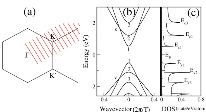
Photoluminescence (PL) is a process in which a SWNT absorbs a photon and then emits a photon. Quantum mechanically, this process can be described as an excitation of an electron to a higher energy band and then a recombination with a hole by emitting a photon. The duration time between the absorption and the emission is typically in the order of 10 ns [59]. The wavelengths of light preferentially absorbed and emitted are determined by the selection rules for optical transition. Over the past few years, PL has become an important technique for the characterization of SWNTs [60]. The ability to probe the electronic structures of a large number of semiconducting SWNTs at the same time has made PL a complementary method to RRS for the characterization of SWNTs. In the most prior PL studies, the SWNT samples were dispersed in a surfactant solution, excited by a lamp source, and the PL spectra were recorded over the near and far IR spectral regions. Generally, in the most of studies, the strongly luminescent peaks are
associated with a emission at ES
11 (from the first conduction band c1 to the first valence
band v1, see Fig. 1.3 (a)) for different semiconducting SWNTs with a strong absorption
at ES
22 (from the second conduction band c2 to the second valence band v2). A very
fast (< 1 ps) relaxation of the photo-excited carrier occurs by emitting a phonon from
E22S to E11S, as shown in Fig. 1.3 (a). In Fig. 1.3 (b), a two-dimensional (2D) map for the PL intensity for a sample of HiPCO SWNTs suspended in SDS and deuterium oxide (D2O) [58] is plotted as functions of absorption (E22S) wave-length (y−axis) and emission
(E11S) wave-length (x−axis). Each strong peak in the 2D map corresponds to a (n, m) SWNT. We can see that the relative PL intensity depends on (n, m) value. It is because that (1) the population for (n, m) SWNTs is different [11] and that (2) the relative matrix elements of PL are strongly chirality dependent [12]. As for (2), we know that PL intensity is relatively strong for large chiral angle near armchair SWNTs [13].
1.4
Experimental background for this study
1.4.1
Resonance Raman window measurement
C. Fantini et al. as our collaborators measured the experimental resonance window for various samples at room temperature and at ambient pressure, using a DILOR XY triple-monochromator spectrometer in a backscattering configuration for measurement, equipped with a liquid N2 cooled charge coupled device (CCD) [9], as shown in Fig 1.4.
In Fig 1.4 (a), the 2D map of the Raman intensity is plotted as a function of the RBM frequency (x−axis) for 76 different excitation laser energies (y−axis). The samples were excited by a tunable laser system composed of a Ti:Sapphire laser, a dye laser, and an Ar-Kr ion laser, in the range 1.52 to 2.71 eV. Along a vertical line of the experimental 2D resonance Raman plot in Fig. 1.4 (a), we get experimental Raman excitation profile (REP) for the individual RBM features for different (n, m) SWNTs present in the sample (see Fig. 1.4 (b)). From these measurements, C. Fantini et al. obtained the experimental resonance window (γEX) values in the resonance Raman profiles as the spectral width of
REP for individual (n, m) SWNTs. Experimental results reveal that the γEXvalue,
repre-senting the lifetime-broadening of the excitonic transition of an individual (n, m) SWNT, strongly depends on the environment of the (n, m) SWNT and on (n, m) values itself in a given sample, which suggests that electron-phonon (or exciton-phonon) coupling depends
(a) 1.8 2 2.2 2.4 2.6 ELaser (eV) 0 0.5 1 Intensity 0 0.5 1 Intensity CoMoCAT (6,5) HiPCO (6,5) bundle Solution Solution bundle (b) (c) γEX γEX
Figure 1.4: (a) The experimental 2D resonance Raman plot (the intensity increases from blue to red) compared with resonance points calculated by the extended tight binding method presented in a Kataura plot (+ for metallic and× for semiconducting nanotubes). SDS-wrapped HiPCO carbon nanotubes in solution were used in the experiment [9]. We can see that, for metallic nanotubes, the experimental peaks are related only to the lower transition energy (EM L
11 ) in the extended Kataura plot. The numbers denote values of
2n+m. The RBM intensity at 310 cm−1is plotted as a function ELfor bundle SWNTs and
for SDS wrapped (6,5) SWNTs in solution for (b) CoMoCAT and (c) HiPCO samples [61]. The experimental resonance window γEX are shown.
on the environment and (n, m) values.
In Fig. 1.4 (b-c), we show the REPs of the RBM at 310 cm−1 observed for (6,5) nanotubes in (b) CoMoCAT [62] and (c) HiPCO [41] samples. Solid circles and open squares denote SDS-wrapped SWNTs in solution and SWNTs within bundles, respec-tively. Solid and dashed lines represent the fit of the REPs to Eq. (1.1.1) for first order single resonance Raman scattering intensity I(EL). The matrix elements for optical
ab-sorption Mel−op, electron-phonon coupling Mel−ph, and optical emission Mel−op are taken
as constants for the fitting. The spectra widths of the REPs correspond to the exper-imental resonance windows γEX. In Chapter 3, we explain how to calculate the matrix
elements, based on the electronic structure by the ETB method explained in Chapter 2. The optical matrix [36] and electron-phonon interaction matrix elements [12] were developed by A. Gr¨uneis and J. Jiang, respectively, who had worked in our group. The
γEX value is determined by fitting the parameter γ of Eq. (1.1.1) to the experimental
points. The fitting was performed not by Lorentzian functions but by making the integral in Eq. (1.1.1), and by considering the numerator as a δ−function integrated in energy
δ(E − (Ea − Ei))dE [9]. For the CoMoCAT nanotubes in solution, the REPs show a
smaller resonance window than those for HiPCO nanotubes in solution. The γEX values
of (6,5) nanotubes for HiPCO and CoMoCAT samples in solution are 63 meV and 40 meV, respectively. Moreover, the resonance window for SWNTs in solution is smaller than that for bundles, which means that there are more relaxation paths for the excited carriers in bundles. For example, the tube-tube interaction may make the carrier relax-ation to other SWNTs possible. When we compare the REPs for HiPCO and CoMoCAT SWNTs in solution, we can see that there are minor differences (up to 80 meV) in the optical transition energies due to the environmental effects which gives rise to the shift of Eii value by the surrounding materials of SWNTs [63]. It should be mentioned that
the γEX for CoMoCAT SWNTs is not always smaller for all (n, m) tubes than the γEX
for HiPCO SWNTs. Thus the 23 meV difference should be considered as a sample- and (n, m)-dependent deviation. We expect that the catalyst or the length of SWNT might not contribute to the resonance window very much because most of catalyst will be re-moved in the purification process and the electron-phonon scattering is also independent of the tube length. In Chapter 4, we will consider the γ value of isolated SWNTs. The calculated γ values for some (n, m) values are compared with the isolated SDS wrapped SWNTs in solution.
1.4.2
G
0band measurement of SWNT
K. K. Kim et al. as our collaborators in Korea observed the dependence of the G0 band in-tensity on the metallicity (being either metallic or semiconducting properties) of SWNTs by RRS with several excitation laser energies of 2.41 eV (514 nm, Ar+ ion laser), 1.96
eV (632.8 nm, He-Ne laser), and 1.58 eV (785 nm, diode laser) [23]. These measure-ments used HiPCO SWNTs sample with diameters ranging from 0.8 to 1.3 nm. For the observation of the metallicity dependence of the G0 band intensity, the pristine HiPCO sample was treated by nitronium ions (NO+2) to remove the metallic (m-) SWNTs. In this treatment, 10 mg of the pristine sample were sonicated for 24 hours in tetramethylene sulfone/chloroform (1:1 by weight) containing 50 mmol nitronium hexafluoroantimonate
0 500 1000 1500 2000 2500 3000 1333 2670 2659 514 nm (2.41 eV) 1591 1337 NHFA-HTT Pristine 200 250 EM11 0.91 0.94 0.99 1.21 RBM 1.35 ES 33 0 500 1000 1500 2000 2500 3000 1309 1317 632.8 nm (1.96 eV) 2605 2621 NHFA-HTT Pristine 1588 200 250 300 0.82 0.87 0.95 1.14 RBM 1.28E M 11E S 22 2400 2600 2622 G'-Band 2608
(a)
(b)
(c)
(d)
(e)
(f)
(g)
(h)
(i)
In
te
n
si
ty
(
a
rb
.
u
n
it
s)
Raman shift (cm
-1)
2400 2600 2670 G'-Band 2659 0 500 1000 1500 2000 2500 3000 1296 785 nm (1.58 eV) 1600 NHFA-HTT Pristine 1303 200 250 ES22 0.91 1.05 1.08 RBM 1.20 1.13 2530 2640 2593 G'-Band 2583 0 500 1000 1500 2000 2500 3000 1333 2670 2659 514 nm (2.41 eV) 1591 1337 NHFA-HTT Pristine 200 250 EM11 0.91 0.94 0.99 1.21 RBM 1.35 ES 33 0 500 1000 1500 2000 2500 3000 1309 1317 632.8 nm (1.96 eV) 2605 2621 NHFA-HTT Pristine 1588 200 250 300 0.82 0.87 0.95 1.14 RBM 1.28E M 11E S 22 2400 2600 2622 G'-Band 2608(a)
(b)
(c)
(d)
(e)
(f)
(g)
(h)
(i)
In
te
n
si
ty
(
a
rb
.
u
n
it
s)
Raman shift (cm
-1)
2400 2600 2670 G'-Band 2659 0 500 1000 1500 2000 2500 3000 1296 785 nm (1.58 eV) 1600 NHFA-HTT Pristine 1303 200 250 ES22 0.91 1.05 1.08 RBM 1.20 1.13 2530 2640 2593 G'-Band 2583Figure 1.5: Raman spectra of the pristine HiPCO sample (black) and the NHFA-treated HiPCO sample (red) at an excitation energy of (a-c) 2.41 eV, (d-f) 1.96 eV, and (g-i) 1.58 eV. The NHFA-treated HiPCO sample was annealed at 900 ◦C. In Figures (b,e,f), the blue and red dotted regions indicate the semiconducting and metallic RBM frequency regions. The G0 band intensity is normalized to the G band peak intensity [23].
(NHFA). While the semiconducting (s-) SWNTs with small diameter range (< 1nm) re-main after the chemical reaction, the m-SWNTs are removed by oxidation in the same diameter range as the s-SWNTs [24].
Figure 1.5 shows strong metallicity dependence of the G0 band intensity of the HiPCO sample. The Raman spectra with excitation laser energy EL = 2.41 eV in Fig. 1.5 (a-c)
show that the pristine HiPCO sample (black lines) consists of both m- and s-SWNTs by analyzing the RBM and G band. After the NHFA treatment followed by thermal annealing at 900 ◦C, the m-SWNTs with small diameters were removed completely, while the s-SWNTs still remained without damage (red lines). This observation was confirmed
by the significant reduction in Breit-Wigner-Fano (BWF) component in the G band, as shown in Fig. 1.5(a,b). In m-SWNTs, the G band becomes soft and the spectra shows asymmetry around the peak position which can be fitted to BWF lines [64]. Then, the G0 band for the NHFA-treated sample was significantly suppressed since the m-SWNTs were removed. If the m-SWNTs with a diameter approximately 0.94 nm were present in the NHFA-treated sample, a strong G0 band intensity would be expected due to the scattering resonance condition for the G0 band at E11M. This suggests that the dependence of the G0 band intensity on the metallicity is dominated by the incident photon resonance of the s-SWNTs. In the case of EL = 1.96 eV in Fig. 1.5 (d-f), more m-SWNTs with large
diameters (> 1nm) remained in the sample, while the s-SWNTs with small diameters were removed after NHFA treatment. The BWF line for the NHFA treatment sample are stronger than that for the pristine sample due to the higher m-SWNT component which can be seen in RBM peak in the metallic resonance condition. In this case, the G0 band intensity becomes stronger. For EL = 1.58 eV in Fig. 1.5 (g-f), the s-SWNTs can be
resonant to ES
22 even after the NHFA treatment. The metallicity dependence of the G0
band is not well recognized in this Raman spectra, because the its G0 band intensity is much smaller than the G band intensity.
In Chapter 5, we will calculate the G0 band intensity for m- and s-SWNT and explain the origin of the metallicity dependence of the G0 band.
1.4.3
G
0band measurement of multi-layer graphene
Finally, we introduce the G0 band measurement of multi-layer graphene which is done by A. Reina in MIT as our collaborator. The graphene samples were prepared on Si substrates with a 300 nm SiO2 over-layer following the procedure given in previous publications
[28, 31]. After graphene deposition by micro-mechanical cleavage [31], the substrates were inspected under an optical microscope and one to three layer (1L, 2L and 3L) graphene regions were identified by both color contrast in the optical microscope and the atomic force microscopy (AFM) height measurements, as shown in Fig. 1.2 (a) (page 5). The Raman spectra were taken with a homemade confocal Raman spectrometer with 7 laser excitation energies from 1.83 eV to 2.72 eV. The laser spot size is 0.5 µm2 and the power of the laser is 1.5 mW at each excitation energy. Intensity calibration of the spectrometer, at each laser energy, was carried with a white tungsten lamp. The experimental spectra
shown here are normalized with the G band intensity for each laser energy. Raman spectra of single, double, and triple layer graphenea at excitation laser energy EL = 2.32 eV are
given in Fig. 1.2 (b). The width and peak position of the G0 band become larger and blue-shifted with increasing number of graphene layers.
In Chapter 6, we will calculate the G0 band spectra shape and intensity for multi-layer graphene.
Chapter 2
Geometry and electronic structure of
SWNT
2.1
Geometry of SWNT
A carbon nanotube rolled up a single graphene sheet is called a single wall carbon nanotube (SWNT), and a carbon nanotube made of concentrically arranged cylinders rolled up several graphene sheets is referred to as a multi-wall carbon nanotube (MWNT). In this thesis, the SWNT is our main work.
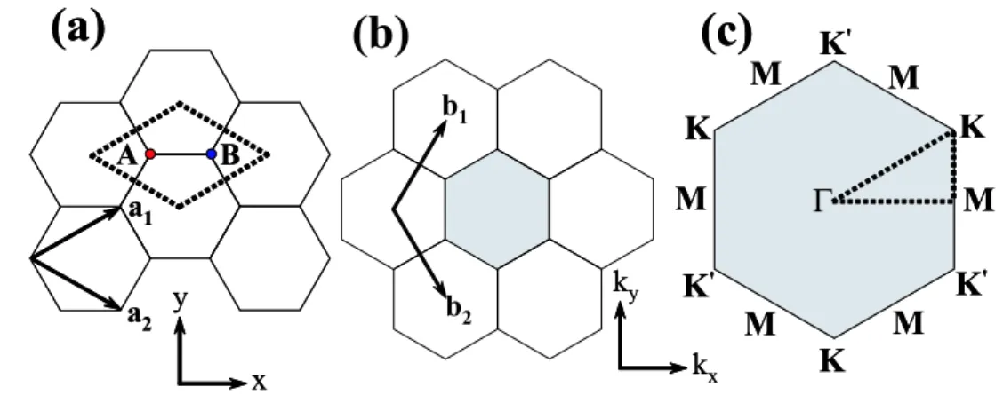
This Section provides some basic definitions about the structure of SWNTs and the construction of one dimensional (1D) Brillouin zone of SWNT in relation to two dimen-sional (2D) Brillouin zone of graphene sheet. A carbon nanotube is a hollow cylinder of 2D graphene sheet. The structure of carbon nanotube has been investigated by the transmission electron microscopy (TEM) [1–3] and the scanning tunneling microscopy (STM) [65], yielding that the carbon nanotube is a seamless cylinder rolled up a graphene sheet with the honeycomb lattice. There are many ways to roll a graphene sheet into a cylindrical carbon nanotube, resulting in different diameter and helical structures of the nanotubes. These carbon nanotubes are defined by the diameter and the chiral angle which means the angle of the hexagon helix around the nanotube axis [5]. The physi-cal properties of SWNTs significantly depend on the structure, including the electronic energy band structure, in particular, their metallic or semiconducting properties [4].
A B a1 a2
(a)
A B a1 a2(a)
(b)
b1 b2(c)
Γ
K
K
K
K
'K
'K
'M
M
M
M
M
M
(c)
Γ
K
K
K
K
'K
'K
'M
M
M
M
M
M
y x y x ky kx ky kxFigure 2.1: (a) The unit cell of graphene sheet is shown as the dotted rhombus. The red and blue dots in the dotted rhombus indicate the A and B sub-lattices, respectively. The real lattice unit vectors a1 and a2 are shown by arrows in the x, y coordinates system.
(b) The first Brillouin zone is by a shaded region. The reciprocal lattice vectors b1 and
b2 are shown by arrows in the kx, ky coordinates. (c) The first Billouin zone of (b). Γ,
K, K0, and M indicate the high symmetry points. In general, energy dispersion relations are obtained along the side of the dotted triangle connecting the high symmetry points, Γ, K and M [5].
2.1.1
Graphene is 2D
Graphene is one atomic layer of graphite. The nearest neighbor distance between two carbon atoms in the graphene sheet is 0.142 nm (aCC). The unit cell and the Brillouin
zone of graphene are expressed, respectively, by a1 and a2 unit vectors in real space, and
by b1 and b2 reciprocal lattice vectors in the k space as shown in Fig. 2.1. In real space,
the unit vectors a1 and a2 are given by:
a1 = √ 3a 2 x +ˆ a 2y,ˆ a2 = √ 3a 2 xˆ− a 2y,ˆ (2.1.1)
where a = √3aCC = 0.246 nm is the lattice constant of graphene sheet. ˆx and ˆy are the
unit vectors in x and y directions of graphene sheet, respectively. These two unit vectors
a1 and a2 make an angle 60◦ in Fig. 2.1 (a). The reciprocal lattice vectors b1 and b2 are
related to the real space vectors a1 and a2 according to following definition:
where δij is the Kronecker delta function. Therefore, the reciprocal unit vectors b1 and
b2 are given by:
b1 = 2π √ 3aˆx + 2π a y,ˆ b2 = 2π √ 3aˆx− 2π a y,ˆ (2.1.3)
where the unit vectors b1 and b2 make an angle 120◦ in Fig. 2.1 (b). These reciprocal
lattice unit vectors define the first Brillouin zone of the graphene sheet and then, the first Brillouin zone has the same hexagon shape as the real space unit cell, but the hexagon orientation is different by 90◦ from each other. In the Brillouin zone as shown in Fig. 2.1 (c), we define three high symmetry points, Γ, K, and M as the center, the hexagonal corner, and the center of a hexagon side, respectively. In general, the energy dispersion of the graphene sheet is calculated for the electron wave vectors on the ΓKM triangle, as shown in Fig. 2.1 (c).
2.1.2
1D unit cell
The structure of a SWNT is conveniently described in terms of its 1D unit cell [5]. The 1D unit cell is defined by the chiral vector Ch and the translation vector T, as shown in
Fig. 2.2. The chiral vector Ch can be represented by the 2D graphene unit vectors a1
and a2 in Eq. (2.1.1):
Ch = na1+ ma2 ≡ (n, m), (2.1.4)
where (n, m) is a pair of integers uniquely defining the particular structure of SWNT (n ≥ m). Many properties of SWNTs such like their electronic band or phonon structures change dramatically with the chiral vector, even though they have similar diameter or similar chiral vector direction [5]. Figure 2.2 shows the unit cell of SWNT with the chiral vector Ch = (4, 2), and the chiral angle θ between the chiral vector Ch and the zigzag
direction (θ = 0), and the unit vector a1 and a2 of the graphene sheet. The chiral angle
θ is given by: θ = tan−1 ³ √3n 2m + n ´ . (2.1.5)
Therefore, the zigzag (n, 0) and armchair (n, n) nanotubes correspond to chiral angle
O A B B'
T
C
h a1 a2 θ4
2
R
O A B B'T
C
h a1 a2 θ4
2
R
T
C
hτ
R(
ψ|τ)
O
ψ
T
C
hτ
R(
ψ|τ)
O
ψ
Figure 2.2: (right) The unrolled graphene sheet of nanotube. OA and OB define the chiral vector Ch and the translation vector T of the SWNT, respectively. Here Ch = (4, 2), T = (4,−5). The chiral angle θ is the angle between a1 and Ch. Therefore, the chiral
angle θ = 0 along the zigzag axis. When we connect four sites O, A, B0, and B, a SWNT can be constructed. The rectangle OAB0B defines the 1D SWNT unit cell. The vector R
indicates a symmetry vector; R = (1,−1). (left) The rotation angel ψ and the translation
τ constitute the basic symmetry operation R = (ψ|τ) for the SWNT. The number of
hexagons per unit cell of the SWNT is denoted by N . For (4,2) SWNT, N = 28 [5].
The diameter dt of a (n, m) SWNT is given by:
dt = Ch π = a π √ n2+ nm + m2, (2.1.6)
where Ch is the length of chiral vector Ch, and a =
√
3aCC.
The translation vector T is normal to the chiral vector Ch and is parallel to the
nanotube axis in the unrolled graphene sheet. The translation vector T corresponds to the vector−−→OB (which is normal to Ch) with the first lattice point B and can be expressed
by unit vectors a1 and a2:
where t1 and t2 are obtained by using the condition Ch· T = 0: t1 = 2m + n dR , t2 =− 2n + m dR , (2.1.8)
where dR = gcd(2n + m, 2m + n), and gcd(i, j) denotes the greatest common divisor of
two integers i and j. The quantity dR is obtained by repeated use of Euclid’s law which
gcd(i, j) =gcd(i− j, j) if i > j. Namely, the quantity d = gcd(n, m) defined by the chiral vector Ch is related to dR= gcd(2n + m, 2m + n) introduced in the translation vector T:
d = gcd(n, m) = gcd(n− m, m), dR= gcd(2n + m, 2m + n) = gcd(n− m, 2m + n) = gcd(n − m, 3m). (2.1.9)
Then, we can relate dR to d:
dR= d, if mod(n− m, 3d) 6= 0, 3d, if mod(n− m, 3d) = 0, (2.1.10)
where mod(i, j) is the remainder (or modulus) of the division of i by j. The unit cell of the SWNT is defined by the chiral vector Ch and the translation vector T. The area of
the SWNT unit cell is given by the absolute value of the vector product of Ch and T,
¯¯Ch× T¯¯. The number of hexagons per unit cell of the SWNT, N is obtained by dividing
the area of the SWNT unit cell by the area of the hexagonal unit cell in the graphene sheet, ¯¯a1× a2¯¯, of Fig. 2.1: N = ¯¯¯¯Ch× T¯¯ a1× a2¯¯ = 2(n2+ nm + m2) dR . (2.1.11)
Consequently, (4, 2) SWNT in Fig. 2.2 has dR = d = 2, T = (4,−5), and N = 28.
The length of the translation vector T is given by:
T =|T| = √ 3a dR √ n2+ nm + m2 = √ 3Ch dR . (2.1.12)
The translational length T is significantly diminished when gcd(n, m) 6= 1. For example, in the case of (9, 9) armchair nanotube, we have dR = 3d = 27, T = (1,−1), and N = 18
and for (9, 0) zigzag nanotube, dR = 9, T = (1,−2), and N = 18, while for (9, 8) chiral
Γ
µ=0 µ=27K
1 T 2π dt 2K
2Γ
µ=0 µ=27K
1 T 2π T 2π T 2π dt 2 dt 2K
2Γ
µ=0 µ=27K
1 T 2π dt 2K
2Γ
µ=0 µ=27K
1 T 2π T 2π T 2π dt 2 dt 2K
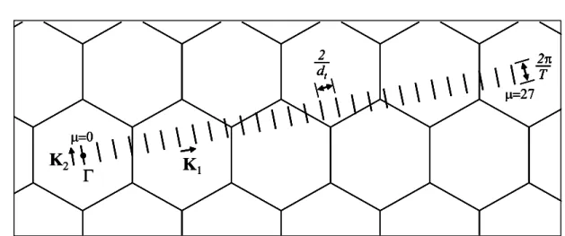
2Figure 2.3: The Brillouin zone of (4,2) SWNT is represented by the set of N = 28 parallel cutting lines. The vector K1 and K2 are the reciprocal lattice vectors which correspond
to Ch and T, respectively. The cutting lines are labeled by the angular momentum index
µ, which defines integer values from 0 to N− 1 = 27. The length of cutting line is defined
by 2π/T = 2π/√21a, where a =√3aCC = 0.246 nm [5].
2.1.3
Cutting line
In Section 2.1.2, we determined the unit cell of SWNT, and in this section, we construct 1D Brillouin zone of a SWNT. Along the circumference vector Ch of the SWNT, any
allowed wave vector k is quantized according to the periodic boundary condition. The wave function of an electron of the SWNT has a boundary-condition-satisfied phase of an integer multiple of 2π for the circumference vector Ch:
k· Ch = 2πµ, (2.1.13)
where µ is the angular momentum of standing wave in the SWNT and is an integer from
µ = 0 to N−1. In terms of the 2D Brillouin zone of graphene sheet, the allowed electronic
states k lie along parallel lines separated by a spacing of 2π/Ch = 2/dt. These lines are
called to cutting lines [66, 67]. Whereas the 1D unit cell of SWNT in the real space is expressed by the chiral vector Ch and the translation vector T, the corresponding vectors
of SWNT in reciprocal space are the reciprocal lattice vectors K1 along the circumferential
direction and K2 along the nanotube axis. Therefore, by using the relations, Ri· Kj =
2πδij, between the real lattice vector Ri (= Ch or T) and the reciprocal lattice vector Kj, the reciprocal lattice vector of SWNT, K1 and K2 are defined by:
T· K1 = 0, Ch· K1 = 2π, Ch· K2 = 0, T· K2 = 2π. (2.1.14)
We substitute Ch and T from Eqs. (2.1.4) and (2.1.7) into Eq. (2.1.14), and then we
express a1 and a2 in K1 and K2 as b1 and b2 by comparing Eqs. (2.1.1) and (2.1.3):
K1 = −t2b1+ t1b2 N , K2 = mb1− nb2 N , (2.1.15)
The reciprocal lattice vectors, K1 and K2 define the separation between the neighboring
cutting lines, and the length of the cutting lines, respectively. The magnitudes of K1 and
K2 are given by:
¯¯K1¯¯= 2π Ch = 2 dt , ¯¯K2¯¯= 2π T , (2.1.16)
Therefore, the N parallel cutting lines are related to discrete value of the angular momen-tum µ in Eq. (2.1.13) and the length of the cutting line ¯¯K2¯¯ determines the periodicity
of the 1D momentum k that has continuous wave vector in the K2 direction for an infinite
SWNT length because of the translational symmetry of the vector T. The allowed wave vector k of a SWNT takes the following form:
k = µK1+ k
K2
K2
, (2.1.17)
where µ = 0,· · · , N − 1, and k = −π/T < k < π/T . The unit cell of the SWNT has N hexagons, and then the first Brillouin zone of the SWNT consists of N cutting lines. In Fig. 2.3, the reciprocal lattice vectors, K1 and K2, for a (4,2) chiral SWNT are shown,
in which N = 28, K1 = (3
√
3, 1)π/14a, and K2 = (1/
√
3, 3)π/7a. For the N cutting lines, N 1D energy bands for each 2D energy band and N 1D phonon dispersions for each phonon mode will appear. The wave vectors in the K2 direction for a SWNT with infinite
tube length are continuous because of its translational symmetry, but, for a SWNT with finite tube length L, the spacing between wave vectors is 2π/L, and its effect on energy band was observed in experiment [68].
2.2
Electronic structure
2.2.1
Electronic structure of graphene
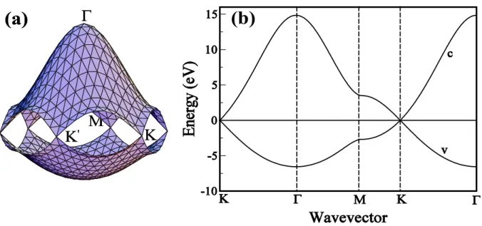
Next, we review a simple tight-binding (STB) model that plays an important role to understand the electronic structure of a graphene sheet and a SWNT. The electronic structure of a SWNT using STB model is derived from that of graphene. For obtaining a good agreement with recent optical experiments, we have to extend the STB model by including the long-range atomic interactions and the σ molecular orbitals, and by optimizing the geometrical structure. The resulting model is hereafter called to extended tight-binding (ETB) model, which we explain below.
In graphene, the π electrons in 2pz orbital are valence electrons which are relevant to
the transport and other optical properties. The π electron has an energy band structure near the Fermi energy, so that electrons can be optically excited from the valence (π) to the conduction (π∗) band.
The electronic energy dispersion relations of a graphene are obtained by solving the single particle Schrodinger equation:
ˆ
HΨb(k, r, t) = i~∂
∂tΨ
b(k, r, t), (2.2.1)
where the single-particle Hamiltonian operator ˆH is given by the following expression:
ˆ
H =− ~
2
2m∇
2+ U (r), (2.2.2)
where∇ is the gradient operator, ~ is the Plank’s constant, m is the electron mass, U(r) is the effective periodic potential, Ψb(k, r, t) is one electron wave function, b (= 1, 2, ..., 8) is
the electron energy band index, k is the electron wave vector, r is the spatial coordinate, and t is time. The one electron wave function Ψb(k, r, t) is constructed from four atomic
orbitals, 2s, 2px, 2py, and 2pz, for the two inequivalent carbon atoms at A and B in the
unit cell of graphene as shown Fig. 2.1 (a), and is approximated by a linear combination of atomic orbitals (LCAO) in terms of Bloch wave function [69]:
Ψb(k, r, t) = eiEb(k)t/~ A,B X s 2s,...,2pXz o Csob (k)Φso(k, r), (2.2.3)
where Eb(k) is the one electron energy, the Cb
so is the wave function coefficient for the
atomic wave function φo(r) for each orbital at the u-th unit cell in a graphene sheet: Φso(k, r) = 1 √ U U X u eik·Rusφ o(r− Rus), (2.2.4)
where the index u (= 1, ..., U ) spans all the U unit cells in a graphene sheet and Rus is
the atomic coordinate for the u−th unit cell and s−th atom. Since the electron wave functions Ψb(k, r, t) should also satisfy Bloch’s theorem, the summation in Eq. (2.2.3) is
taken only for the Bloch wave function Φso(k, r) with the same value of k. The eigenvalue
Eb(k) as a function of k is given by:
Eb(k) = hΨ(k)| ˆH|Ψ(k)i
hΨ(k)|Ψ(k)i . (2.2.5)
Substituting Eq. (2.2.3) into Eq. (2.2.5), we obtain the following equation:
Eb(k) = X s0o0 X so Csb0∗o0(k)Hs0o0so(k)Csob (k) X s0o0 X so Csb0∗o0(k)Ss0o0so(k)Csob (k) , (2.2.6)
where the transfer integral Hs0o0so(k) and overlap integral Ss0o0so(k) matrices are given by:
Hs0o0so(k) = 1 U U X u eik·(Rus−Ru0s0) Z φ∗o0(r− Ru0s0)Hφo(r− Rus)dr, Ss0o0so(k) = 1 U U X u eik·(Rus−Ru0s0) Z φ∗o0(r− Ru0s0)φo(r− Rus)dr. (2.2.7)
When we fix the values of the n×n (n = 8) matrices Hs0o0so(k) and Ss0o0so(k) in Eq. (2.2.7)
for a given electron wave vector k, the wave function coefficient Cb∗
s0o0(k) is optimized so
as to minimize Eb(k). The coefficient Cb∗
s0o0(k) as a function of k is a complex variable
with a real and a complex part, and both Csb0∗o0(k) and Csob (k) are independent each other.
Taking a partial derivative for Cb∗
s0o0(k) while fixing the coefficient Csob (k), we can get the
variational condition for finding the minimum of the ground state energy [5]:
∂Eb(k)
∂Cb∗ s0o0(k)
= 0. (2.2.8)
(2.2.8) becomes: ∂Eb(k) ∂Cb∗ s0o0(k) = X so Hs0o0so(k)Csob (k) X s0o0 X so Csb0∗o0(k)Ss0o0so(k)Csob (k) − X s0o0 X so Csb0∗o0(k)Hs0o0so(k)Csob (k) ³X s0o0 X so Csb0∗o0(k)Ss0o0so(k)Csob (k) ´2 X so Ss0o0so(k)Csob (k) = X so Hs0o0so(k)Csob (k)− E b(k)X so Ss0o0so(k)Csob (k) X s0o0 X so Csb∗0o0(k)Ss0o0so(k)Csob (k) = 0, (2.2.9)
and then upon multiplying both side of Eq. (2.2.9) by X
s0o0
X
so
Csb0∗o0(k)Ss0o0so(k)Csob (k), we
can obtain simple following equation: X so Hs0o0so(k)Csob (k)− E b(k)X so Ss0o0so(k)Csob (k) = 0. (2.2.10)
Eq. (2.2.10) is expressed by a matrix form when we define the Cb
so(k) as a column vector: ³ H(k)− Eb(k)S(k) ´ Cb(k) = 0, Cb(k) = Cb 2sA .. . Cb 2pB z , (b = 1, · · · , 8). (2.2.11)
The eigenvalues of Hs0o0so(k) are calculated by solving the following secular equation for
each k: det h H(k)− Eb(k)S(k) i = 0, (2.2.12)
where Eq. (2.2.12) gives eight eigenvalues of Eb(k) for the energy band index b = 1,· · · , 8 for a given electron wave vector k. Considering four atomic orbitals per one carbon atom (2s, 2px, 2py, 2pz) and two carbon atomic site (A, B) per unit cell of a graphene sheet, we
obtain the 8× 8 Hamiltonian Hs0o0so(k) and overlap Ss0o0so(k) matrices, and then these
matrices are expressed by 2× 2 sub-matrix for two sub-atoms:
H(k) = HAA(k) HAB(k) HBA(k) HBB(k) and S(k) = SAA(k) SAB(k) SBA(k) SBB(k) , (2.2.13)
where HAA (HBB) and HAB (HBA) are expressed by 4× 4 sub-matrix for four orbitals.
The matrix elements between 2pz orbital and 2s, 2px, and 2py are zero because of the
odd (even) function 2pz (2s, 2px, and 2py) of z for the both cases of HAA (HBB) and HAB
(HBA): HAA(k) = h2sA|H|2sAi h2sA|H|2pA xi h2sA|H|2pAyi h2sA|H|2pAzi h2pA x|H|2sAi h2pAx|H|2pAxi h2pxA|H|2pAyi h2pAx|H|2pAzi h2pA y|H|2sAi h2pAy|H|2pAxi h2pyA|H|2pAyi h2pAy|H|2pAzi h2pA z|H|2sAi h2pAz|H|2pAxi h2pzA|H|2pAyi h2pAz|H|2pAzi = h2sA|H|2sAi 0 0 0 0 h2pA x|H|2pAxi 0 0 0 0 h2pAy|H|2pAyi 0 0 0 0 h2pA z|H|2pAzi = HBB(k), HAB(k) = h2sA|H|2sBi h2sA|H|2pB xi h2sA|H|2pByi h2sA|H|2pBzi h2pA x|H|2sBi h2pAx|H|2pBxi h2pxA|H|2pByi h2pAx|H|2pBzi h2pA y|H|2sAi h2pAy|H|2pAxi h2pyA|H|2pByi h2pAy|H|2pBzi h2pA z|H|2sAi h2pAz|H|2pBxi h2pzA|H|2pByi h2pAz|H|2pBzi = h2sA|H|2sBi h2sA|H|2pB xi h2sA|H|2pByi 0 h2pA x|H|2sBi h2pAx|H|2pxBi h2pAx|H|2pByi 0 h2pA y|H|2sAi h2pAy|H|2pxAi h2pAy|H|2pByi 0 0 0 0 h2pA z|H|2pBzi = THBA∗ (k). (2.2.14)
In a flat graphene sheet, these matrices are partitioned into the 6× 6 and 2 × 2 sub-matrices corresponding to the σ and π molecular orbitals, respectively, because the atomic orbital 2s, 2px, and 2py are even functions of z, which parallel to the graphene sheet, while
the 2pz orbital is an odd function of z.
The STB model neglects the σ molecular orbitals and the long-range atomic inter-actions, R > aCC. Therefore, in the STB model, we solve for the 2× 2 sub-matrix to
determine the dispersion relation Eb(k) and the electron wave function coefficients for the