®
Altera Corporation 1
PCI Master/Target MegaCore Function with DMA
November 1999, ver. 3.02 Data Sheet
PCI Bus Interface
3
Operation
Features
■ pci_a MegaCore™ function implementing a 32-bit peripheral component interconnect (PCI) master/target interface■ Optimized for the FLEX® 10K architecture
■ Extensive hardware testing using:
– HP E2925A PCI Bus Exerciser and Analyzer – FLEX 10K PCI prototype board
– Validated against common PCI chipsets such as: Intel 430 and 440 chipsets, and DEC PCI-to-PCI bridges
■ Dramatically shortens design cycles
■ FLEX 10K PCI prototype board included
■ Includes test vectors for user simulation
■ OpenCore™ feature allows designers to instantiate and simulate designs in the MAX+PLUS® II software prior to licensing
■ Uses approximately 1,000 FLEX logic elements (LEs), e.g., 35% the capacity of an EPF10K50 device
■ PCI master features:
– Memory read/write – Bus parking
– Fully integrated DMA engine including address counter register, byte counter register, control and status register, and interrupt status register
– Configurable interrupt source, including DMA terminal count, master abort, target abort, and local side interrupt
– 64-byte (16 double words or DWORDs) RAM buffer implemented in FLEX 10K embedded array blocks (EABs) – Zero-wait-state PCI read and write burst transactions
■ PCI target features:
– Type zero configuration space – Parity error detection
– Memory read/write and configuration read/write – Target retry and disconnect
– 1 Mbyte to 2 Gbytes of parameterized target memory space
■ Configuration registers:
– Parameterized: device ID, vendor ID, class code, revision ID, base address zero, subsystem ID, subsystem vendor ID – Non-parameterized: command, status, header type, latency
timer, interrupt pin, interrupt line
PCI Master/Target MegaCore Function With DMA Data Sheet
3
Operation PCI Bus InterfaceIntroduction
This data sheet provides operating information for the pci_a MegaCore function and includes the following topics:New in Version 2.0... 3
General Description ... 4
Compliance Summary... 5
PCI Bus Signals... 7
Local Side Signals... 10
Function Prototype ... 12
Parameters... 13
Functional Description ... 14
Sustained Tri-State Signal Operation ... 15
Master Device Signals & Signal Assertion ... 15
Target Device Signals & Signal Assertion ... 16
Parity Signal Operation... 17
Bus Master Commands ... 18
Configuration Registers ... 18
Vendor ID Register (Offset = 00 Hex) ... 20
Device ID Register (Offset = 02 Hex) ... 20
Command Register (Offset = 04 Hex) ... 21
Status Register: (Offset = 06 Hex) ... 22
Revision ID Register (Offset = 08 Hex) ... 23
Class Code Register (Offset = 09 Hex) ... 23
Latency Timer Register (Offset = 0D Hex) ... 23
Header Type Register (Offset = 0E Hex) ... 24
Base Address Register Zero (Offset = 10 Hex)... 24
Subsystem Vendor ID Register (Offset = 2C Hex) ... 25
Subsystem ID Register (Offset = 2E Hex) ... 25
Interrupt Line Register (Offset = 3C Hex) ... 25
Interrupt Pin Register (Offset = 3D Hex)... 26
Minimum Grant Register (Offset = 3E Hex) ... 26
Maximum Latency Register (Offset = 3F Hex) ... 26
PCI Bus Transactions ... 27
Target Transactions... 27
Configuration Transactions ... 35
Master Transactions... 36
DMA Operation... 42
Target Address Space ... 43
Internal Target Registers Memory Map... 43
DMA Registers ... 44
Initializing DMA Transfers from the Local Side ... 50
DMA Transactions ... 47
General Programming Guidelines... 54
Applications ... 58
PCI SIG Protocol Checklists... 60
PCI Master/Target MegaCore Function With DMA Data Sheet
New in Version 2.0
The pci_a function version 2.0 includes the following enhancements:
■ Additional device support
■ Local-side initiated DMA
■ Parameterized base address registers (BARs)
■ Byte-wide selection during external target write transfers
■ Use of l_holdn during external target transactions
■ Larger DMA byte counter register
More Device Support
The pci_a function supports a wide range of devices and packages including the following FLEX 10K devices:
■ EPF10K30RC240
■ EPF10K30RC208
■ EPF10K30AQC240
■ EPF10K30AQC208
■ EPF10K40RC240
■ EPF10K40RC208
■ EPF10K50RC240
■ EPF10K100ARC240
■ EPF10K30BC356
■ EPF10K50BC356
■ EPF10K100ABC356
1 Additional device support will become available as new devices are released. Please check the Altera world-wide web site at http://www.altera.com for latest device support.
Local-Side Initiated DMA
To perform a DMA burst transfer using the pci_a function, appropriate values must be written to the DMA registers to setup the transfer. In prior versions of the pci_a function, the host or a PCI master device was required to write to DMA registers. However, pci_a version 2.0 also allows DMA read and write transactions directly from the local side device. See “Initializing DMA Transfers from the Local Side” on page 50 for more information.
PCI Master/Target MegaCore Function With DMA Data Sheet
3
Operation PCI Bus InterfaceParameterized BARs
The BAR0 is parameterized to provide optimum efficiency for memory allocation.In pci_a version 1.3, the BAR0 address space is a constant 1 Mbyte of contiguous address space divided into two 512 Kbytes of memory space. However, in pci_a version 2.0 and later, users can vary the BAR0 address space from 1 Mbyte to 2 Gbytes of contiguous memory.
See “Base Address Register Zero (Offset = 10 Hex)” on page 24 for more information.
Byte-Wide Selection during Target Write Transfers
During target transfers, the PCI cben[3..0] bus signals are byte enable signals, indicating which byte carries meaningful data. Bit 3 of the cben[3..0] bus applies to byte 3, and bit 0 applies to byte 0. Likewise in pci_a version 2.0, the additional local-side l_ben[3..0] bus signals buffer the cben[3..0] bus signals and inform the local-side logic which byte carries meaningful data during external target write transactions.
l_holdn for External Target Write Transactions
In pci_a version 1.3 the local application is required to supply or accept data within two clock cycles. In version 2.0, a slower application can assert l_holdn to extend the period necessary to transfer the data.
Larger DMA Byte Counter Register
The DMA byte counter register was increased from 16 bits to 17 bits. As a result, the master DMA engine may initiate memory transfers up to 128 Kbytes for each DMA transaction.
General Description
The pci_a MegaCore function provides a timely solution for integrating 32-bit PCI peripheral devices, and is fully tested to meet the requirements of the PCI specification. The pci_a function is optimized for the
FLEX 10K device family, reducing the design task and enabling designers to focus efforts on the custom logic surrounding the PCI interface (ordering code: PLSM-PCI/A). Figure 1 shows the pci_a symbol.
PCI Master/Target MegaCore Function With DMA Data Sheet Figure 1. pci_a Symbol
Compliance Summary
The pci_afunction is compliant with the requirements specified in the PCI Special Interest Group’s (SIG) PCI Local Bus Specification,
Revision 2.1, and Compliance Checklist, Revision 2.1. The pci_a function has successfully completed extensive hardware validation testing to ensure robustness and PCI bus compliance. The testing was performed using the following hardware and software:
■ Altera FLEX 10K PCI prototype board
■ BlueWater Systems WinDK (Windows NT-based) software driver
■ HP E2925A PCI Bus Exerciser and Analyzer
The testing was performed in a fully-loaded PCI bus. In addition to the HP E2925A PCI Bus Exerciser and Analyzer and the Altera PCI prototype board, PCI bus agents such as the host bridge, Ethernet network adapter, and video card tested the function using data-intensive applications. The extensive testing ensures that the pci_a function operates flawlessly under the most stringent conditions.
PCI Signals CLK RSTN REQN GNTN IDSEL AD[31..0]
CBEN[3..0]
PAR FRAMEN_IN FRAMEN_OUT IRDYN DEVSELN TRDYN_IN TRDYN_OUT STOPN_IN STOPN_OUT INTAN PERRN SERRN
PCI_A
L_IRQN L_HOLDN L_REQ L_CLK L_RESET L_ADR[30-BAR0_RW_BITS..0]
L_DAT_OUT[31..0]
L_DAT_IN[31..0]
L_BEN[3..0]
L_ACKN L_CSN L_RDN L_WRN L_DMA_ACR_WR L_DMA_BCR_WR L_DMA_CSR_WR L_DMA_DAT_IN[31..0]
L_DMA_CSR_OUT[6..0]
L_DMA_ACR_OUT[31..0]
L_DMA_BCR_OUT[16..0]
L_DMA_ISR_OUT[4..0]
Local Signals
BAR0_RW_BITS=12 CLASS _CODE=H"FF0000"
DEVICE_ID=H"0001"
DEVICE_VEND_ID=H"1172"
REVISION_ID=H"02"
SUBSYSTEM_ID=H"0000"
SUBSYSTEM_VEND_ID=H"0000"
TARGET_DEVICE="EPF10K30RC240"
PCI Master/Target MegaCore Function With DMA Data Sheet
3
Operation PCI Bus Interface The pci_a function performs master and target transactions to and fromthe Altera PCI prototype board. Along with typical burst and single-cycle transactions, the pci_a function runs various interrupt cycles and initiates different abnormal terminations. In addition to checking for data
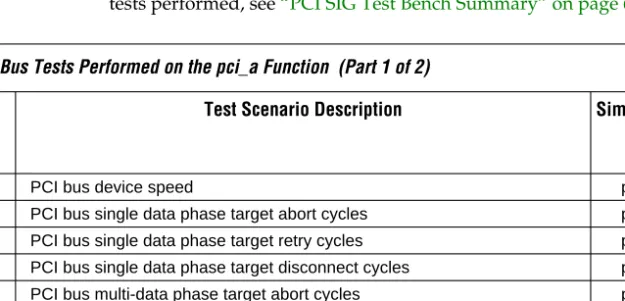
integrity, the HP E2925A PCI Bus Exerciser and Analyzer was used to ensure that the PCI bus is free of protocol violation. Each iteration of the test program transfers over 6.5 billion data bytes between the host memory and the pci_a-based EPF10K30 device. The test procedure was done overnight, thus accounting for hundreds of iterations. The tests were repeated across multiple PCI platforms to ensure compatibility with various chipsets. Table 1 shows a list of hardware platforms with which the pci_a function was tested at the time of this document printing.
In addition to all the hardware testing, the pci_a function was verified using the applicable scenarios listed in Table 2. For a detailed listing of tests performed, see “PCI SIG Test Bench Summary” on page 66.
Table 1. pci_a Hardware Verified Platforms
Platform Chipset CPU
Speed (MHz)
PCI Bus Speed (MHz)
Dell OptiPlex XM 5166 Intel 430 NX 166 33
Dell OptiPlex GX Pro Intel 440FX PCISet (Bus 0) 200 33
DEC21052-AB PCI-PCI bridge (Bus 1) 200 33
Dell OptiPlex GXL 5166 Intel 430 FX PCISet 166 33
U-tron (Pentium/MMX) Intel 430 VX PCISet 166 33
Table 2. PCI Bus Tests Performed on the pci_a Function (Part 1 of 2) PCI Test
Scenario Number
Test Scenario Description Simulation File Name Note (1)
1.1 PCI bus device speed pcicc101
1.2 PCI bus single data phase target abort cycles pcicc102
1.3 PCI bus single data phase target retry cycles pcicc103
1.4 PCI bus single data phase target disconnect cycles pcicc104
1.5 PCI bus multi-data phase target abort cycles pcicc105
1.6 PCI bus multi-data phase target retry cycles pcicc106
1.7 PCI bus multi-data phase target disconnect cycles pcicc107
1.8 PCI bus multi-data phase & trdyn cycles pcicc108
1.9 PCI bus data parity error single cycles pcicc109
PCI Master/Target MegaCore Function With DMA Data Sheet
Note:
(1) The file extension depends on the type of simulation file used, e.g., Simulator Channel File (.scf), Vector File (.vec), or VHDL file.
(2) This test is not required by the PCI SIG PCI Local Bus Specification, Revision 2.1, and therefore does not have a test number.
PCI Bus Signals
The following PCI bus signals are used by the pci_a function:
■ Input—Standard input-only signal.
■ Output—Standard output-only signal.
■ Bidirectional—Tri-state input/output signal.
■ Sustained tri-state—Signal that is driven by one agent at a time (e.g., device or host operating on the PCI bus). An agent that drives a sustained tri-state pin low must actively drive it high for one clock cycle before tri-stating it. Another agent cannot drive a sustained tri- state signal any sooner than one clock cycle after it is released by the previous agent.
■ Open-drain—Signal that is wire-ORed with other agents. The signaling agent asserts the open-drain signal, and a weak pull-up resistor deasserts the open-drain signal. The pull-up resistor may take two or three PCI bus clock cycles to restore the open-drain signal to its inactive state.
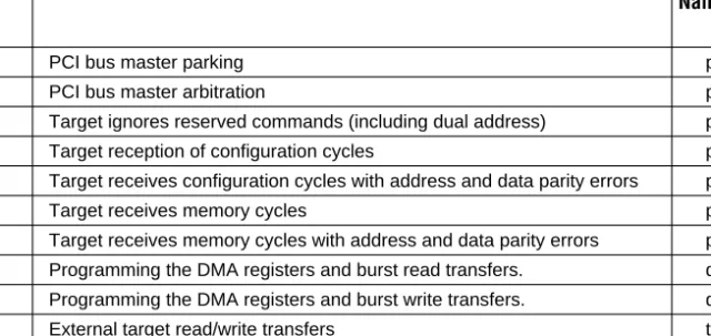
PCI Test Scenario Number
Test Scenario Description Simulation File Name, Note (1)
1.13 PCI bus master parking pcicc113
1.14 PCI bus master arbitration pcicc114
2.5 Target ignores reserved commands (including dual address) pcicc205
2.6 Target reception of configuration cycles pcicc206
2.8 Target receives configuration cycles with address and data parity errors pcicc208
2.9 Target receives memory cycles pcicc209
2.10 Target receives memory cycles with address and data parity errors pcicc210 Note (2) Programming the DMA registers and burst read transfers. dma_rd Note (2) Programming the DMA registers and burst write transfers. dma_wr
Note (2) External target read/write transfers trg_xrw
Table 2. PCI Bus Tests Performed on the pci_a Function (Part 2 of 2)
3
Operation PCI Bus Interface Table 3 summarizes the PCI bus signals interfacing the pci_a function tothe PCI bus. See “Local Side Signals” on page 10 for information on local side signals.
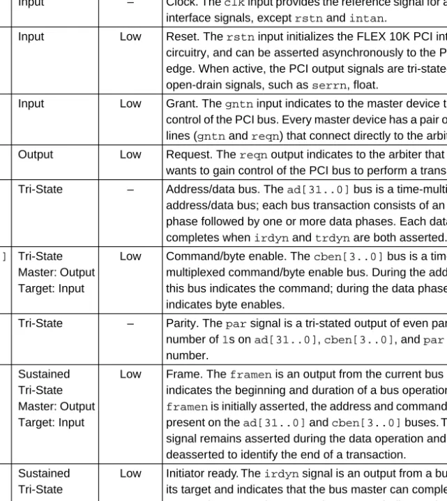
Table 3. PCI Signals Interfacing the pci_a to the PCI Bus (Part 1 of 2)
Name Type Polarity Description
clk Input – Clock. The clk input provides the reference signal for all other PCI interface signals, except rstn and intan.
rstn Input Low Reset. The rstn input initializes the FLEX 10K PCI interface circuitry, and can be asserted asynchronously to the PCI bus clk edge. When active, the PCI output signals are tri-stated and the open-drain signals, such as serrn, float.
gntn Input Low Grant. The gntn input indicates to the master device that it has control of the PCI bus. Every master device has a pair of arbitration lines (gntn and reqn) that connect directly to the arbiter.
reqn Output Low Request. The reqn output indicates to the arbiter that the master wants to gain control of the PCI bus to perform a transaction.
ad[31..0] Tri-State – Address/data bus. The ad[31..0] bus is a time-multiplexed address/data bus; each bus transaction consists of an address phase followed by one or more data phases. Each data phase completes when irdyn and trdyn are both asserted.
cben[3..0] Tri-State Master: Output Target: Input
Low Command/byte enable. The cben[3..0] bus is a time-
multiplexed command/byte enable bus. During the address phase this bus indicates the command; during the data phase this bus indicates byte enables.
par Tri-State – Parity. The par signal is a tri-stated output of even parity. The number of 1s on ad[31..0], cben[3..0], and par is an even number.
framen Note (1)
Sustained Tri-State Master: Output Target: Input
Low Frame. The framen is an output from the current bus master that indicates the beginning and duration of a bus operation. When framen is initially asserted, the address and command signals are present on the ad[31..0] and cben[3..0] buses. The framen signal remains asserted during the data operation and is
deasserted to identify the end of a transaction.
irdyn Sustained Tri-State Master: Output Target: Input
Low Initiator ready. The irdyn signal is an output from a bus master to its target and indicates that the bus master can complete a data transaction. In a write transaction, irdyn indicates that valid data is on the ad[31..0] bus. In a read transaction, irdyn indicates that the master is ready to accept the data on the ad[31..0] bus.
devseln Sustained Tri-State
Low Device select. Target asserts devseln to indicate that the target has decoded its own address.
Note:
(1) To allow the pci_a function to pass the PCI set-up time requirement, the framen, trdyn, and stopn signals are split into two unidirectional (input, output) signals. For example, the PCI signal trdyn is connected to the input trdyn_in and the output trdyn_out. The input trdyn_in is connected to a dedicated input on the FLEX 10K device, and the output trdyn_out is connected to an I/O pin on the FLEX 10K device.
The PCI bus and FLEX 10K devices allow IEEE Std. 1149.1 Joint Test Action Group (JTAG) boundary-scan testing (BST). To use IEEE Std.
1149.1 BST, designers should connect the PCI bus JTAG pins with the FLEX 10K device JTAG pins. See Table 4.
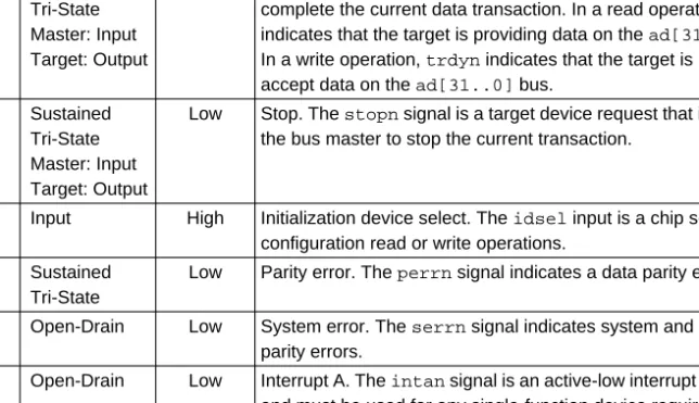
Name Type Polarity Description
trdyn Note (1)
Sustained Tri-State Master: Input Target: Output
Low Target ready. The trdyn signal indicates that the target can complete the current data transaction. In a read operation, trdyn indicates that the target is providing data on the ad[31..0] bus.
In a write operation, trdyn indicates that the target is ready to accept data on the ad[31..0] bus.
stopn Note (1)
Sustained Tri-State Master: Input Target: Output
Low Stop. The stopn signal is a target device request that indicates to the bus master to stop the current transaction.
idsel Input High Initialization device select. The idsel input is a chip select for configuration read or write operations.
perrn Sustained Tri-State
Low Parity error. The perrn signal indicates a data parity error.
serrn Open-Drain Low System error. The serrn signal indicates system and address parity errors.
intan Open-Drain Low Interrupt A. The intan signal is an active-low interrupt to the host, and must be used for any single-function device requiring an interrupt capability.
Table 3. PCI Signals Interfacing the pci_a to the PCI Bus (Part 2 of 2)
Table 4. Optional IEEE Std. 1149.1 Signals
Name Type Polarity Description
TCK Input High Test clock. The TCK input is used to clock test mode and test data in and out of the device.
TMS Input High Test mode select. The TMS input is used to control the state of the Test Access Port (TAP) control in the device.
TDI Input High Test data. The TDI input is used to shift the test data and instruction into the device.
TDO Output High Test data. The TDO output is used to shift the test data and instruction out of the device.
3
Operation PCI Bus InterfaceLocal Side Signals
Table 5 summarizes the pci_a function signals that interface the pci_a function to the local side peripheral device(s).
Table 5. pci_a Signals Interfacing the pci_a Function to the Local Side (Part 1 of 3)
Name Type Polarity Description
l_irqn Input Low Local side interrupt request. The local side peripheral device asserts l_irqn to signal a PCI bus interrupt. For example, when the local side peripheral device requires a DMA transfer, it could use the l_irqn input to request servicing from the host.
l_holdn Input Low Local hold. During master transactions, l_holdn suspends the current DMA transfer. As long as l_holdn is active, data transfers cannot occur between the pci_a function and the local side peripheral device. During target transactions, the assertion of l_holdn extends the external target transfers. If l_holdn is not asserted, the pci_a function expects data to be supplied to or received from the local side on the second clock after l_csn is asserted.
l_req Input High Local DMA request. After the DMA has been loaded with valid data, the local side peripheral device asserts l_req, which signals the pci_a function to start the PCI DMA operation.
l_dat_in[31..0] Input – Local data bus input. The l_dat_in[31..0] input is driven active by the local side peripheral device during pci_a-initiated DMA write transactions (i.e., local side DMA read transactions) and PCI bus target read transactions.
l_dat_out[31..0] Output _ Local data bus output. The pci_a function drives the l_dat_out[31..0] output during pci_a-initiated DMA read transactions (i.e., local side DMA write transactions) and PCI target write transactions.
l_ben[3..0] Output Low Local byte enable. The l_ben[3..0] outputs are driven by the pci_a function to indicate the byte select during target write transfers.
l_adr[30-BAR0_RW_BITS..0] Output – Local target address. The l_adr[30-
BAR0_RW_BITS..0] outputs represent address of the target transaction to the local side peripheral device.
l_csn Output Low Local target chip select. When active, l_csn notifies the peripheral device of an impending target transaction. The
Name Type Polarity Description
l_rdn Output Low Read. The pci_a function asserts l_rdn to signal a read access to the local side peripheral device. The pci_a function uses the l_rdn for reading from peripheral device target registers and for PCI DMA write transactions. For target read operations, the pci_a function asserts the l_csn and l_rdn signals. For DMA write operations, the pci_a function asserts the l_ackn and l_rdn signals.
l_wrn Output Low Write. The pci_a function asserts l_wrn to signal a write access to the local side peripheral device. The pci_a function uses the l_wrn output for writing to peripheral device target registers and for PCI DMA read
transactions. For a write operation to the local side, pci_a asserts either l_csn and l_wrn for target accesses, or l_ackn and l_wrn for DMA read accesses.
l_ackn Output Low Local DMA acknowledge. When low, l_ackn notifies the local side peripheral device that it has been granted a DMA read or write transaction. The peripheral device can then transfer data to or from the PCI bus through the pci_a function.
l_clk Output – Local PCI clock. The l_clk is a buffered version of the PCI bus clock and is used by the local side peripheral device to synchronize all control logic to the pci_a function.
l_reset Output High Local reset. The pci_a function asserts the l_reset output to reset the local side peripheral device. The l_reset output is active during a PCI master reset and follows the state of the l_rst bit (bit 2 of the DMA control status register).
l_dma_acr_wr Input High Local DMA address counter register write. The local side asserts l_dma_acr_wr to signal a write access to the DMA address counter register. When l_dma_acr_wr is high, the data on l_dma_in[31..0] bus is written into the dma_acr register.
l_dma_bcr_wr Input High Local DMA byte counter register write. The local side asserts l_dma_bcr_wr to signal a write access to the DMA byte counter register. When l_dma_bcr_wr is high, the data on l_dma_dat_in[31..0] bus is written into the dma_bcr register.
Table 5. pci_a Signals Interfacing the pci_a Function to the Local Side (Part 2 of 3)
3
Operation PCI Bus InterfaceFunction Prototype
The Altera Hardware Description Language (AHDL) Function Prototype of the pci_a function is shown below:
FUNCTION pci_a (clk, framen_in, gntn, idsel, l_dat_in[31..0], l_holdn, l_irqn, l_req, rstn, stopn_in, trdyn_in, l_dma_acr_wr, l_dma_bcr_wr, l-dma_csr_wr, l_dma_dat_in[31..0])
WITH (SUBSYSTEM_ID, SUBSYSTEM_VEND_ID, DEVICE_ID, DEVICE_VEND_ID, CLASS_CODE, REVISION_ID, BAR0_RW_BITS, TARGET_DEVICE)
RETURNS (framen_out, l_ackn,
l_adr[30-BAR0_RW_BITS..0], l_clk, l_csn,
l_dat_out[31..0], l_ rdn, l_reset, l_wrn, stopn_out, trdyn_out, ad[31..0], cben[3..0], devseln, intan, irdyn, par, perrn, reqn, serrn; l_dma_csr_out[6..0], l_dma_acr_out[31..0], l_dma_bcr[16..0],
l_dma_isr_out[4..0], l_ben[3..0]);
Name Type Polarity Description
l_dma_csr_wr Input High Local DMA control status register write. The local side asserts l_dma_csr_wr to signal a write access to the DMA control/status registers. When l_dma_csr_wr is high, the data on l_dma_dat_in[31..0] bus is written into the dma_csr register.
l_dma_dat_in[31..0] Input – Local DMA data in. While one of the DMA write signals (l_dma_acr_wr, l_dma_bcr_wr, or l_dma_csr_wr) is asserted, the l_dma_dat_in[31..0] supplies the data to be written to the corresponding DMA register.
l_dma_csr_out[6..0] Output – Local DMA control status registers out. Direct output of the DMA control/status register.
l_dma_acr_out[31..0] Output _ Local DMA address counter registers out. Direct output of DMA the address counter registers.
l_dma_bcr_out[16..0] Output _ Local DMA byte counter registers out. Direct output of the DMA byte counter register.
l_dma_isr_out[4..0] Output _ Local DMA interrupt status registers out. Direct output of the DMA interrupt status register.
Table 5. pci_a Signals Interfacing the pci_a Function to the Local Side (Part 3 of 3)
Parameters
The pci_a parameters—except BAR0_RW_BITS and TARGET_DEVICE—set read-only PCI bus configuration registers in the pci_a function; these registers are called device identification registers. See “Configuration Registers” on page 18 for more information on device ID registers.
The BAR0_RW_BITS parameter controls the number of read/write bits instantiated for BAR0, and according to the PCI specification, the number of read/write bits instantiated for BAR0 controls the memory address range reserved by the BAR0. The value of the BAR0_RW_BITS parameter must be between 1 and 12. The TARGET_DEVICE parameter ensures that the most optimized design is used for a particular device and package, which ensures timing compliance of the target device. For the most updated list of support devices and packages, refer to the readme.htm file included with the pci_a function. Table 6 describes the parameters of the pci_a function.
Table 6. Parameters
Name Format Default Value Description
BAR0_RW_BITS Decimal 12 BAR address space size
TARGET_DEVICE String "EPF10K30RC240" Device selection CLASS_CODE 24-bit Hex H"FF0000" Class code register DEVICE_ID 16-bit Hex H"0001" Device ID register DEVICE_VEND_ID 16-bit Hex H"1172" Device vendor ID register REVISION_ID 8-bit Hex H"02" Revision ID register SUBSYSTEM_ID 16-bit Hex H"0000" Subsystem ID register SUBSYSTEM_VEND_ID 16-bit Hex H"0000" Subsystem vendor ID register
3
Operation PCI Bus InterfaceFunctional Description
The pci_a function consists of three main components:
■ A defined 64-byte PCI bus configuration register space and master control logic
■ PCI bus target interface control logic, including target decode and register read/write signals
■ Embedded DMA control engine, which operates with four registers and includes a 64-byte (16 DWORD) RAM buffer, and local side interface DMA control logic, including read/write control and PCI bus arbitration for master/target accesses
Figure 2 shows the pci_a function’s block diagram.
Figure 2. pci_a Function Block Diagram
par perrn serrn
Parity Checking & Generation Target Interface
Master Interface PCI Address/
Data Buffering Configuration Registers
DMA Registers Local Data Buffering
Local Side DMA Access Control
Local Side Target Access Control pci_a
clk rstn
idsel
ad[31..0]
cben[3..0]
reqn gntn intan framen irdyn devseln trdyn stopn
64-Byte RAM Buffer (EAB)
l_adr[18..0]
l_csn l_rdn l_wrn
l_dat_in[31..0]
l_dat_out[31..0]
l_ackn l_clk l_reset l_holdn l_req l_irqn
l_ben[3..0]
l_dma_acr_wr l_dma_bcr_wr l_dma_csr_wr l_dma_dat_in[31..0]
l_dma_csr_out[6..0]
l_dma_acr_out[31..0]
l_dma_bcr_out[16..0]
l_dma_isr_out[4..0]
Sustained Tri-State Signal Operation
The PCI specification defines signals that are constantly sampled by different bus agents yet driven by one agent at a time as sustained tri-state signals. For example, framen is constantly sampled by different PCI bus targets (to detect the start of a transaction), and yet driven by one PCI bus master at a time.
For sustained tri-state signals, the PCI specification requires one clock cycle to drive the signals inactive before being tri-stated. The PCI specification also requires that any sustained tri-state signal being released, such as the master device releasing ad[31..0] after asserting the address on a read operation, be given a full clock cycle to tri-state before another device can drive it.
The PCI specification defines a turn-around cycle as the clock cycle where a sustained tri-state signal is being tri-stated so that another bus agent can drive it. Turn-around cycles prevent contention on the bus.
Master Device Signals & Signal Assertion
Figure 3 illustrates the PCI-compliant master device signals interfacing pci_a with the PCI bus. The signals are grouped by functionality, and signal directions are illustrated from the perspective of the pci_a function operating as a master on the PCI bus.
A pci_a master sequence begins with the assertion of reqn to request mastership of the PCI bus. After receiving gntn from the arbiter (usually the PCI host bridge) and after the bus idle state is detected, the pci_a function initiates the address phase by asserting framen and driving both the PCI address on ad[31..0] and the bus command on cben[3..0]for one clock cycle.
When the pci_a master is ready to present data on the bus, it asserts irdyn. At this point, the pci_a function’s master logic monitors the control signals driven by the target device. (A target device is determined by the decoding of the address and command signals presented on the PCI bus during the address phase of the transaction.) The target device drives the control signals devseln, trdyn, and stopn to indicate one of the following:
■ The data transaction has been decoded and accepted.
■ The target device is ready for the data operation. (When both trdyn and irdyn are active, a data DWORD is clocked from the sending to the receiving device.)
■ The master device should stop the current transaction.
3
Operation PCI Bus Interface Figure 3. pci_a Master Device SignalsTarget Device Signals & Signal Assertion
Figure 4 illustrates the PCI-compliant target device signals interfacing the pci_a function with the PCI bus. The signals are grouped by
functionality, and signal directions are illustrated from the perspective of the pci_a function operating as a target on the PCI bus.
A pci_a target sequence begins when the master device asserts framen and drives the address of the target and the command on the PCI bus.
When the target device decodes its address on the PCI bus, it asserts devseln to indicate to the master that it has accepted the transaction. The master will then assert irdyn to indicate to the target device that:
■ For a read operation, the master device can complete a data transaction.
■ For a write operation, valid data is on the ad[31..0] bus.
When the pci_a functions as the selected target device, it will drive the control signals devseln, trdyn, and stopn as discussed in “Master Device Signals & Signal Assertion” on page 15.
pci_a PCI-Compliant Master Device framen
irdyn trdyn stopn devseln Interface
Control Signals
gntn reqn Arbitration
Signals
Address, Data &
Command Signals
par ad[31..0]
cben[3..0]
perrn serrn
intan
Error Reporting Signals
Interrupt Request Signal System
Signals
clk rstn idsel
As a target device, the pci_a function only supports single-cycle accesses;
therefore, the pci_a function simultaneously drives stopn and trdyn active. When qualified by an active irdyn signal, a data word is clocked from the sending to the receiving device.
Figure 4. pci_a Target Device Signals
Parity Signal Operation
All bus cycles include parity. Every device that transmits on the
ad[31..0] bus must also drive the par signal, including master devices outputting the address. Because parity on the PCI bus is even, the number of logic 1s on ad[31..0], cben[3..0], and par must be even. Parity checking is not required, but can be enabled through the agent’s PCI command register. Address parity errors are presented on the serrn output, and data parity errors are presented on the perrn output. The par bit lags the ad[31..0]bus by one clock cycle, and parity error signals lag the par bit by one clock cycle; thus, parity error signals lag the address or data by two clock cycles.
pci_a PCI-Compliant
Target Device System
Signals
clk rstn
perrn serrn
intan
Error Reporting Signals
Interrupt Request Signal
Address, Data &
Command Signals
par ad[31..0]
cben[3..0]
framen irdyn trdyn stopn devseln Interface
Control Signals
idsel
3
Operation PCI Bus InterfacePCI Bus Commands
Table 7 summarizes the PCI bus commands that are supported by the pci_a function.
The pci_a function supports memory read/write and configuration read/write commands. When operating as a master device, the pci_a function executes standard memory read and write operations. When operating as a target, the pci_a function responds to standard memory read and write transactions. The pci_a function also responds to configuration read and write operations.
Configuration Registers
Each logical PCI bus device includes a block of 64 configuration DWORDs reserved for the implementation of its configuration registers. The format of the first 16 DWORDs is defined by the PCI SIG’s PCI Compliance Checklist, Revision 2.1, which defines two header formats, type one and type zero. Header type one is used for PCI-to-PCI bridges; header type zero is used for all other devices, including the pci_a function.
Table 8 displays the defined 64-byte configuration space. The registers within this range are used to identify the device, control PCI bus
functions, and provide PCI bus status. The shaded areas indicate registers that are supported by the pci_a function.
Table 7. PCI Bus Command Support Summary
cben[3..0] Value Bus Command Cycle Target Support Master Support
0110 Memory read v v
0111 Memory write v v
1010 Configuration read v
1011 Configuration write v
Table 9 summarizes the pci_a-supported configuration registers address map. Read/write refers to the status at run time, i.e., from the perspective of other PCI bus agents. Designers can set some of the read-only registers at design time by setting the parameters when the pci_a function is instantiated in the MAX+PLUS II software. For example, the device ID register value can be modified from its default value by changing the DEVICE_ID parameter in the MAX+PLUS II software. The specified default state is defined as the state of the register when the PCI bus is reset.
Table 8. PCI Bus Configuration Registers
Address Byte
3 2 1 0
00H Device ID Vendor ID
04H Status Register Command Register
08H Class Code Revision ID
0CH BIST Header Type Latency Timer Cache Line Size
10H Base Address Register 0
14H Base Address Register 1
18H Base Address Register 2
1CH Base Address Register 3
20H Base Address Register 4
24H Base Address Register 5
28H Card Bus CIS Pointer
2CH Subsystem ID Subsystem Vendor ID
30H Expansion ROM Base Address Register
34H Reserved
38H Reserved
3CH Maximum
Latency
Minimum Grant Interrupt Pin Interrupt Line
Table 9. pci_a-Supported Configuration Registers Address Map (Part 1 of 2) Address Offset
(Hexadecimal)
Range Reserved (Hexadecimal)
Bytes Used/
Reserved
Read/Write Mnemonic Register Name
00 00-01 2/2 Read ven_id Vendor ID
02 02-03 2/2 Read dev_id Device ID
04 04-05 2/2 Read/Write comd Command
06 06-07 2/2 Read/Write status Status
08 08-08 1/1 Read rev_id Revision ID
3
Operation PCI Bus InterfaceVendor ID Register (Offset = 00 Hex)
Vendor ID is a 16-bit read-only register that identifies the manufacturer of the device (e.g., Altera for the pci_a function). The value of this register is assigned by the PCI SIG; the default value of this register is the Altera vendor ID value, which is 1172 hex. However, by setting the
DEVICE_VEND parameter (see Table 6), designers can change the value of the vendor ID register to their PCI SIG-assigned vendor ID value. See Table 10.
Device ID Register (Offset = 02 Hex)
Device ID is a 16-bit read-only register that identifies the type of device.
The value of this register is assigned by the manufacturer (e.g., Altera assigned the value of the device ID register for the pci_a function). The default value of the device ID register is 0001 hex; however, designers can change the value of the device ID register by setting the parameter DEVICE_ID (see Table 6 on page 13).
Address Offset (Hexadecimal)
Range Reserved (Hexadecimal)
Bytes Used/
Reserved
Read/Write Mnemonic Register Name
09 09-0B 3/3 Read class Class code
0D 0D-0D 1/1 Read/Write lat_tmr Latency timer
0E 0E-0E 1/1 Read header Header type
10 10-13 4/4 Read/Write bar0 Base address register
zero
2C 2C-2D 2/2 Read sub_ven_id Subsystem vendor ID
2E 2E-2F 2/2 Read sub_id Subsystem ID
3C 3C-3C 1/1 Read/Write int_ln Interrupt line
3D 3D-3D 1/1 Read int_pin Interrupt pin
3E 3E-3E 1/1 Read min_gnt Minimum grant
3F 3F-3F 1/1 Read max_lat Maximum latency
Table 9. pci_a-Supported Configuration Registers Address Map (Part 2 of 2)
Table 10. Vendor ID Register Format
Data Bit Mnemonic Read/Write Definition
15..0 ven_id Read PCI vendor ID
Command Register (Offset = 04 Hex)
Command is a 16-bit read and write register that provides basic control over the ability of the pci_a function to respond to and/or perform PCI bus accesses. See Table 11
.
Table 11. Command Register Format
Data Bit Mnemonic Read/Write Definition
0 Unused – –
1 mem_ena Read/Write Memory access enable. When high, mem_ena enables the pci_a function to respond to the PCI bus memory accesses as a target. Because the DMA registers are set via memory target accesses, the mem_ena bit must be set as part of the initialization operation for the pci_a function to perform DMA transfers.
2 mstr_ena Read/Write Master enable. When high, mstr_ena enables the pci_a function to acquire mastership of the PCI bus.
For the pci_a function to perform DMA transfers, the mstr_ena bit must be set as a part of the initialization operation.
5..3 Unused – –
6 perr_ena Read/Write Parity error enable. When high, perr_ena enables the pci_a function to report parity errors via the perrn output.
7 Unused – –
8 serr_ena System error enable. When high, serr_ena enables the pci_a function to report address parity errors via the serrn output. However, to signal a system error, the perr_ena bit must also be high.
15..9 Unused – –
3
Operation PCI Bus InterfaceStatus Register: (Offset = 06 Hex)
Status is a 16-bit register that provides the status of bus-related events.
Read transactions to the status register behave normally. However, write transactions are different from typical write transactions in that bits in the status register can be cleared but not set. A bit in the status register is cleared by writing a logic one to that bit. For example, writing the value 4000 hex to the status register clears bit number 14 and leaves the rest of the bits unchanged. The default value of the status register is 0400 hex.
See Table 12.
Table 12. Status Register Format
Data Bit Mnemonic Read/Write Definition
7..0 Unused – –
8 dat_par_rep Read/Write Data parity reported. When high, dat_par_rep indicates that during a read transaction the pci_a function asserted the perrn output as a master device, or that during a write transaction the perrn was asserted by a target device. This bit is high only when the perr_ena bit (bit 6 of the command register) is also high.
10..9 devsel_tim Read Device select timing. The devsel_tim bits indicate target access timing of the pci_a function via the devseln output. The pci_a function is designed to be a slow target device.
11 Unused – –
12 tar_abrt Read/Write Target abort. When high, tar_abrt indicates that the current target device transaction has been terminated.
13 mstr_abrt Read/Write Master abort. When high, mstr_abrt indicates that the current master device transaction has been terminated.
14 serr_set Read/Write Signaled system error. When high, serr_set indicates that the pci_a function drove the serrn output active, i.e., an address phase parity error has occurred.
15 det_par_err Read/Write Detected parity error. When high, det_par_err indicates that the pci_a detected either an address or data parity error. Even if parity error reporting is disabled (via perr_ena), the pci_a function will set the det_par_err bit.
Revision ID Register (Offset = 08 Hex)
Revision ID is an 8-bit read-only register that identifies the revision number of the device. The value of this register is assigned by the manufacturer (e.g., Altera for the pci_a function). Therefore, the default value of the revision ID register is set as the revision number of the pci_a function. See Table 13. However, designers can change the value of the revision ID register by setting the REVISION_ID parameter (see Table 6).
Class Code Register (Offset = 09 Hex)
Class code is a 24-bit read-only register divided into three sub-registers:
base class, sub-class, and programming interface. Refer to the PCI Local Bus Specification, Revision 2.1 for detailed bit information. See Table 14.
The default value of the class code register is FF0000 hex; however, designers can change the value by setting the CLASS_CODE parameter (see Table 6).
Latency Timer Register (Offset = 0D Hex)
The latency timer register is an 8-bit register with bits 2, 1, and 0 tied to GND. The register defines the maximum amount of time, in PCI bus clock cycles, that the pci_a function can retain ownership of the PCI bus. After initiating a transaction, the pci_a function decrements its latency timer by one on the rising edge of each clock. The default value of the latency timer register is 00 hex. See Table 15
.
Table 13. Revision ID Register Format
Data Bit Mnemonic Read/Write Definition
7..0 rev_id Read PCI revision ID
Table 14. Class Code Register Format
Data Bit Mnemonic Read/Write Definition
23..0 class Read Class code
Table 15. Latency Timer Register Format
Data Bit Mnemonic Read/Write Definition
2..0 lat_tmr Read Latency timer register 7..3 lat_tmr Read/Write Latency timer register
3
Operation PCI Bus InterfaceHeader Type Register (Offset = 0E Hex)
Header type is an 8-bit read-only register that identifies the pci_a function as a single-function device. The default value of the header type register is 00 hex. See Table 16.
Base Address Register Zero (Offset = 10 Hex)
Depending on the value of the BAR0_RW_BITS parameter, base address register zero (BAR0) consists of registers ranging from 12 to 1 bit. The BAR0_RW_BITS can be set when the pci_a function is instantiated, and determines the base memory address of the pci_a target space. This process is done in accordance with the PCI Local Bus Specification, Revision 2.1., which states that the number of bits implemented as read/write registers defines the amount of memory address space reserved by the BAR. Power-up software can determine how much address space a device requires by writing a value of all 1s to the BAR and then reading the value back. To specify the required address space, the pci_a function will return 0s in all the lower bits. The amount of required address space is generally a function of the value of the BAR0_RW_BITS parameter, i.e., assuming BAR0_RW_BITS = n, the reserved address space is 2(32-n) bytes. For example, when BAR0_RW_BITS = 4, the reserved address space is 2 (32-4) bytes, or 256 Mbytes. See Table 17.
Table 16. Header Type Register Format
Data Bit Mnemonic Read/Write Definition
7..0 header Read PCI header type
Table 17. Base Address Register Format (Part 1 of 2)
Data Bit Mnemonic Read/Write Definition
0 mem_ind Read Memory indicator. The mem_ind bit indicates whether the register is I/O or a memory address decoder. In the pci_a function, the mem_ind bit is tied to GND, which indicates a memory address decoder.
2..1 mem_type Read Memory type. The mem_type bits indicate the type of memory that can be implemented in the pci_a function memory address space. These bits are tied to GND, which indicates that the memory block can be located anywhere in the 32-bit address space.
3 pre_fetch Read Memory prefetchable. The pre_fetch bit indicates whether the block of memory defined by BAR0 is
Subsystem Vendor ID Register (Offset = 2C Hex)
Subsystem vendor ID is a 16-bit read-only register that identifies add-in cards designed by different vendors but with the same functional device on the card. The value of this register is assigned by the PCI SIG. See Table 18. The default value of the subsystem vendor ID register is 0000 hex; however, designers can change the value by setting the SUBSYSTEM_VEND_ID parameter (see Table 6).
Subsystem ID Register (Offset = 2E Hex)
Subsystem ID register identifies the subsystem; the value of this register is defined by the subsystem vendor, i.e., the designer. See Table 19. The default value of the subsystem ID register is 0000 hex; however, designers can change the value by setting the SUBSYSTEM_ID parameter (see Table 6).
Interrupt Line Register (Offset = 3C Hex)
The interrupt line register consists of an 8-bit register that defines to which system interrupt request line (on the system interrupt controller) the intan output is routed. The interrupt line register is written to by the system software on power-up; the default value is FF hex. See Table 20.
Data Bit Mnemonic Read/Write Definition
31-BAR0_RW_BITS Unused – –
31..(32-BAR0_RW_BITS) bar0 Read/write Base address register 0.
Table 17. Base Address Register Format (Continued) (Part 2 of 2)
Table 18. Subsystem Vendor ID Register Format
Data Bit Mnemonic Read/Write Definition
15..0 sub_vend_id Read PCI subsystem/vendor ID
Table 19. Subsystem ID Register Format
Data Bit Mnemonic Read/Write Definition
15..0 sub_id Read PCI subsystem ID
Table 20. Interrupt Line Register Format
Data Bit Mnemonic Read/Write Definition
7..0 int_ln Read/write Interrupt line register
3
Operation PCI Bus InterfaceInterrupt Pin Register (Offset = 3D Hex)
The interrupt pin register consists of an 8-bit read-only register that defines the pci_a function’s PCI bus interrupt request line to be intan. The default value of the interrupt pin register is 01 hex. See Table 21.
Minimum Grant Register (Offset = 3E Hex)
Minimum grant register consists of an 8-bit read-only register that defines the length of time the pci_a function would like to retain mastership of the PCI bus. The value set in this register indicates the required burst period length in 250-ns increments. The pci_a function requests a timeslice of 4 microseconds. The default state of the minimum grant register is 10 hex. See Table 22.
Maximum Latency Register (Offset = 3F Hex)
The maximum latency register is an 8-bit read-only register that defines the frequency in which the pci_a function would like to gain access to the PCI bus. The value of the maximum latency register is set to 00 hex, which indicates that the pci_a function has no major requirements for
maximum latency. See Table 23.
Table 21. Interrupt Pin Register Format
Data Bit Mnemonic Read/Write Definition
7..0 int_pin Read Interrupt pin register
Table 22. Minimum Grant Register Format
Data Bit Mnemonic Read/Write Definition
7..0 min_gnt Read Minimum grant register
Table 23. Maximum Latency Register Format
Data Bit Mnemonic Read/Write Definition
7..0 max_lat Read Maximum latency register
PCI Bus Transactions
This section describes pci_a PCI bus transactions. The following items should be considered when reading the diagrams in this section:
■ All pci_a DMA accesses to the PCI bus are quad-byte, or 32-bit transfers; therefore, all byte enables are active for the duration of master data transfers. During pci_a external target write accesses, the transfers are byte selectable.
■ Although Figures 5 through 16 show PCI bus signals as tri-stated when not driven by the pci_a function, they are actually high due to the pull-up resistors used to keep sustained tri-state signals at a logic high while the signals are not being driven by a PCI bus agent.
The pci_a function accesses the PCI bus for three types of transactions:
■ Target
■ Configuration
■ Master
Target Transactions
The sequence of events for the beginning of all target transfers is exactly the same. A target read or write transaction begins after the master acquires mastership of the PCI bus. The master device then asserts framen and drives the address on the ad[31..0] bus and command on the cben[3..0] bus. The pci_a function latches the address and command signals on the first clock edge when framen is asserted and starts decoding the address.
Target Read Transactions
The pci_a function supports two types of target read transactions:
■ Internal target read—Target read transaction from the internal DMA registers
■ External target read—Target read transaction from the local side target memory space
The sequence of events in both target read transactions is identical;
however, the timing is not. (See “External Target Read Transaction” on page 29 for more information.) A target read transaction from the local side target memory space requires more time because the pci_a function must wait for the local side to supply it with data.
3
Operation PCI Bus Interface Internal Target Read TransactionImmediately after the address phase (clock four), the master deasserts framen and asserts irdyn, indicating both of the following:
■ The transaction contains a single data phase.
■ The master device is ready to read the data that the pci_a function has presented on the ad[31..0] bus.
The master device tri-states the ad[31..0]bus in clock five after the pci_a function latches the address. The pci_a function can drive the ad[31..0] bus beginning in clock six. If the master is attempting a burst access, it will keep both framen and irdyn signals asserted. However, because the pci_a function does not support target bursts, it will assert stopn to indicate a disconnect to the master. The master will subsequently end the transaction by deasserting framen and asserting irdyn for one clock cycle.
In Figure 5, the pci_a function asserts devseln in clock seven, which indicates to the master device that pci_a has claimed the transaction. The devseln is then sampled by the master device on the rising-edge of clock eight, which is slow decode, as defined by the PCI specification. Figure 5 shows the timing of a pci_a internal target read transaction.
Figure 5. Internal Target Read Transaction
reqn (Master) gntn (Arbiter)
1 2 3 4 5 6 7 8 9 10
clk
200 ns 300 ns
0 ns
Byte Enable
100 ns
ad[31..0] (pci_a) Address D0
cben[3..0] (Master) 0110
irdyn (Master) framen (Master) perrn (Master) par (pci_a)
stopn (pci_a) trdyn (pci_a) devseln (pci_a)
11
Add-Par Par-D0
Perr
In Figure 5, the pci_a asserts trdyn and stopn in clock eight to indicate that valid data is on the ad[31..0] bus and a disconnect is desired. Data is transferred during clock eight when irdyn and trdyn are active and latched by the master device on the rising-edge of clock nine. In the case of an attempted burst transfer, the PCI specification requires that a target device that does not support burst transfers must issue a disconnect during the first data phase. Because of the PCI specification, the pci_a function always asserts stopn and trdyn at the same time.
The master drives the par active in clock five for address parity, and the pci_a function drives par active in clock nine for data parity. In a target read transaction, the master device drives the perrn signal to indicate data parity errors.
In clock nine, because the data has been sampled, the pci_a function releases the ad[31..0]bus and the master releases cben[3..0].The devseln, trdyn, and stopn signals are driven high in clock nine and released by the pci_a one clock later. Thus, the sustained tri-state signal requirement is met, i.e., driving the signal high for one clock cycle before releasing it.
External Target Read Transaction
The sequence of events in an external target read transaction is identical to an internal target read transaction. However, because a DMA access to the local side takes precedence over any other access to the local side, an external target read transaction is allowed to complete only when the DMA is idle. If an external target read transaction is received by the pci_a function while the DMA is not idle, the pci_a function signals a retry.
Because the pci_a function must wait for the local side to supply it with data, a target read transaction from the local side target memory space (external target read) requires more time. If the local logic cannot supply the data within one clock after l_csn and l_rdn are asserted, l_holdn can be asserted low to halt the data transfers. The l_holdn signal may be driven low until the data is presented on the l_dat_in[31..0] bus.
1 PCI specification requires that the first data phase of a target transaction completes within 16 clock cycles. The local device must ensure that the PCI specification is not violated by an excessively long l_holdn assertion.
3
Operation PCI Bus Interface Figures 6 shows the timing of a pci_a external target read transaction.Figure 6. External Target Read Transaction
Figure 7 illustrates an external target read transfer where l_holdn is used to insert additional wait states on the local side. Unable to supply data immediately when l_csn and l_rdn are asserted, the local logic asserts l_holdn in clock eight for two clock cycles. The local side supplies the data on the l_dat_in[31..0] bus in clock 10 and deasserts l_holdn. The pci_a function latches the data internally on the rising edge of clock 11 and deasserts l_rdn. The l_csn is deasserted one clock later. The pci_a drives the data on the PCI bus one clock after it latches it from the local side (clock 13). Because l_holdn is registered, the local side must follow the tSU timing requirements (provided by the MAX+PLUS II Timing Analyzer) when it drives l_holdn.
1 To avoid excessive latency, the PCI specification requires that PCI target devices complete the initial data transaction within 16 clocks after framen is asserted. (The local logic must ensure that this PCI specification is met.) Therefore, l_holdn cannot be held active for more than 10 clock cycles.
1 2 3 4 5 6 7 8 9 10 11 12
clk
D0 Address
0110 Byte Enable
Add-Par Par-D0
Perr ad[31..0]
cben[3..0]
par perrn
irdyn framen
devseln trdyn stopn
Valid Address
l_adr[18..0]
l_dat_in[31..0] D0
l_rdn l_csn
Figure 7. External Target Read Transaction with l_holdn Asserted
Target Write Transactions
The pci_a function supports two types of target write transactions:
■ Internal target write: Target write to internal DMA registers
■ External target write: Target