INVITED PAPER
Special Section on Analog Circuits and Related SoC Integration TechnologiesDigitally Assisted Analog and RF Circuits
Kenichi OKADA†a),Senior Member
SUMMARY In this paper, the importance and perspective for the digitally-assisted analog and RF circuits are discussed, especially related to wireless transceivers. Digital calibration techniques for compensating I/Q mismatch, IM2, and LO impairments in cellular, 2.4 GHz WiFi, and 60 GHz WiGig transceivers are introduced with detailed analysis and cir- cuit implementations. Future technology directions such as the shift from digitally-assisted analog circuit to digitally-designed analog circuit will also be discussed.
key words:CMOS, wireless, reconfigurable, RF, analog, Digital assistance
1. Introduction
Early generation of CMOS transistors were widely used for digital circuits. CMOS transistors have obtained high frequency capability by the process miniaturization, and CMOS transistors are now capable of more than 100 GHz operation. 60 GHz full wireless transceivers can be imple- mented even by a 65 nm CMOS technology [1]–[7]. Re- cently, 260-GHz amplifier [8], 300-GHz fundamental os- cillator [9], 482-GHz oscillator (third-harmonic use) [10], 1-THz detector [11], 28 Gbps transceiver [5], and 35-dBm CMOS power amplifier [12] have been reported. On the other hand, the miniaturized CMOS transistors suffer from the process variation, larger noise, lower supply volt- age, lower gain, etc. Thus, the digitally-assisted analog circuit technique is a key technology for realizing high- performance CMOS analog and RF circuits. Due to the pro- cess miniaturization, the digital circuits can be shrunk, and more digital circuits can be used for the analog-block cali- bration and compensation. In terms of total layout area and power consumption, the digitally-assisted analog circuits can make them smaller than the traditional analog circuits, which often perform much better for many aspects with cali- bration and compensation techniques,e.g., mismatch, offset, linearity, voltage and temperature stability, etc.
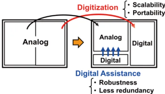
Due to the less cost of digital circuits, analog functions have been replaced by digital circuits,i.e.,digitization.Dig- ital assistancefor analog circuits anddigitizationof analog circuits are very important trend of mixed-signal System-on- Chip (SoC) design. Figure 1 explains this situation. By ap- plying the digital-assistance, analog circuits can obtain ro-
Manuscript received December 9, 2014.
Manuscript revised February 27, 2015.
†The author is with the Department of Physical Electronics, Tokyo Institute of Technology, 2-12-1-S3-27 Ookayama, Meguro- ward, Tokyo 152-8552, Japan.
a) E-mail: [email protected] DOI: 10.1587/transele.E98.C.461
Fig. 1 Digital assistance and Digitization.
Fig. 2 Trend for digitization.
bustness for PVT variation, which contributes to less redun- dancy in design. Balanced and higher performance can be achieved since the analog circuits can be almost free from various aspects of performance trade-offand degradation by the PVT variation, etc.
In addition, the digitization has to be well considered for the mixed-signal SoC design. Sometimes, analog cir- cuits should be replaced by digital circuits instead of the digitally-assisted analog circuits since some kinds of signal processing are much fitter for digital-domain one. If dig- itized, it can be easily transferred to another process tech- nology as well as digital circuits, and will be more advan- tageous in a scaled process technology. The process porta- bility and scalability are the most important features of dig- itized circuits.
Figure 2 shows some examples of the digitization of analog function. The analog filter suffers from linearity, noise, GBW limitation, PVT variation, etc, which often be- comes a performance limiter in wireless system. On the other hand, in the digital filter, complicated filter functions can be easily realized. Even though it suffers from the quantization noise, much more ideal characteristics can be Copyright c⃝2015 The Institute of Electronics, Information and Communication Engineers
ing is now realized as orthogonal frequency domain multi- plex (OFDM). Due to the technology advancement of ADC, the sampling frequency can be increased, and IF blocks in a hetero-dyne receiver can be digitized, known as low-IF ar- chitecture. As explained above, many analog functions have been digitized due to results of architecture-level optimiza- tion.
In terms of digital assistance, many system-level ap- proaches have been applied in wireless systems to satisfy complicated requirements for the wireless communication.
One of the key ideas is a mutual re-use of transmitter and receiver for calibration, which means that a receiver can be used for calibrating a transmitter,vice versa. Several cali- bration and compensation techniques will be introduced in the following sections.
2. Digital Calibration and Compensation in Wireless Systems
2.1 Impairments in Wireless Systems
The quality of wireless communication can be easily de- graded by non-idealities such as antenna reflection, fad- ing, interferer, propagation loss, loss variation, non-linearity of up/down-conversion blocks, phase noise of local oscil- lator, frequency offset between local oscillators in trans- mitter and receiver, NF of down-conversion blocks, I/Q mismatch of both transmitter and receiver, LO leakage, DC offset, gain/phase flatness, group delay, and these PVT variation, etc. Thus, historically, many digital assis- tance/compensation techniques have been utilized in wire- less systems.
In terms of calibration and compensation scheme, the non-idealities can be classified as follows.
• Mismatch in differential block
— LO leakage in TX
— DC offset in RX
— IM2 in RX
• Mismatch between I (in-phase) and Q (quadrature- phase) blocks
— Image signal
— Frequency dependent image by baseband ana- log filters
• Non-linearity
— IM3, IM5 in PA
— TX-to-RX distance
— Fading
— Antenna reflection
The mismatch between identical blocks is one of the most common impairments in CMOS integrated circuits.
However, fortunately, the mismatch can be easily mitigated by the digitally-assisted calibration. The mismatch calibra- tion mechanisms are indispensable for recent wireless stan- dards. For example, UMTS/LTE direct-conversion receivers require an IIP2 of more than 70 dBm, which is almost im- possible without any mismatch calibration for differential blocks [13]. I/Q mismatch is caused by a mismatch between I (in-phase) and Q (quadrature-phase) down/up-conversion signal paths in both amplitude and phase. Calibration and compensation techniques are also available for the I/Q mis- match issue, which will be revisited later. In terms of digital compensation, even the non-linearity can be compensated.
A digital pre-distortion is sometimes applied to compensate PA non-linearity. PVT variation can also be mitigated by the digitally-assisted calibration and compensation techniques, and some examples will be introduced later. The environ- mental variation is very common issues for wireless sys- tems, and various system-level compensation techniques are applied such as automatic gain control (AGC), frequency domain equalizer (FDE), OFDM, diversity, etc. The wire- less systems suffer from both the impairment of transceiver and environmental variation, so enormous numbers of tech- niques have historically been developed to mitigate the non- idealities. One of the most important trends of compensa- tion in wireless systems is the digitization not digital assis- tance. If the compensation process can possibly be digitized, i.e., the impairment can be compensated in digital domain, it has been implemented in the digital domain in almost every case. For example, the equalization is done in digital do- main by a common FIR filter, the carrier recovery has been moved from digital assistance to digital-domain implemen- tation, and I/Q mismatch calibration is often replaced by a digital-domain compensation. It should be emphasized that the digitization, rather than the digital assistance, has to be considered for a further performance extension, which re- quires architecture-level and system-level approaches.
2.2 Target SNR
Here, a required SNR is discussed to understand the require- ment for the calibration and compensation. If only the ther- mal noise is assumed, the bit error rate (BER) can be calcu- lated withS NRas follows.
Fig. 3 Bit error rate (BER) considering thermal noise.
M−PSK BER ≃ 1
log2Merfc
(√
S NRsin π M )
(1) M−QAM
BER ≃ 2 log2M
( 1− 1
√M )
erfc
√ 3S NR 2(M−1)
(2) Figure 3 plots the relationship betweenS NRandBER.
BERcan be improved by forward error correction (FEC) us- ing Reed-Solomon (RS), low-density parity check (LDPC), Turbo, etc. Finally, the packet error rate (PER) is deter- mined byBERwith FEC depending on the packet lengthn as follows.
PER=1−(1−BER)n (3)
Usually, aPERof 10−2=1% can be acceptable even if the overhead of automatic repeat request (ARQ) is considered.
As expressed in Eq. (3), a BER of 10−6 is required with FEC for a 10,000-bit packet. Even though the gain of FEC depends on the coding scheme, for example, aBERof 10−3 is usually required without FEC.
SNR for a BER of 10−3 is also shown in Fig. 3,e.g., 9.8 dB for QPSK, 16.5 dB for 16QAM, and 22.5 dB for 64QAM. This SNR has to be maintained through both trans- mitter and receiver, so a 3-dB higher SNR is required for each transmitter and receiver at least. Thus, about 26 dB SNR is required for 64QAM transmitter. However, this SNR is also degraded from the non-linearity, phase noise, I/Q mismatch, frequency flatness, etc. In case of transmitter, the non-linearity of PA should be dominant for maximizing the output power, so other SNR degradation factors should be enough lower than the non-linearity limited SNR. For ex- ample, at least 35 dB has to be maintained in each the image rejection ratio degraded by the I/Q mismatch, the integrated phase noise with consideration of carrier tracking, the FIR equalization with sufficient number of taps.
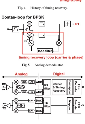
2.3 Carrier Recovery
The carrier and timing recovery is a good example to know the digitization of wireless transceiver. Figure 4 shows a simplified transition from analog-type carrier and timing re- covery [14] to digital-type one [15].
Fig. 4 History of timing recovery.
Fig. 5 Analog demodulator.
Fig. 6 Recent digital transceiver.
Firstly, the analog-type carrier and timing recovery was employed, known as Costas-loop. Figure 5 shows a typi- cal implementation of Costas-loop for BPSK demodulation.
One of the most significant weaknesses is longer acquisi- tion time, which limits the preamble length. In addition, it is usually unstable under small received signal.
To improve the tracking capability of analog recov- ery, a digitally-assisted architecture was considered, which seems like the relationship between the analog PLLs using PFD, CP and LPF, and the all-digital PLLs using TDC and digital LPF. A shorter acquisition time can be realized by the digital assistance. However, still analog-domain phase tracking is required in this architecture.
For further improvement, a complete digital-domain carrier frequency and symbol timing recovery is usually em- ployed in recent wireless transceivers as shown in Fig. 6.
The recovery circuit is placed after RX filter, which is used for equalization and I/Q mismatch compensation. The re- covery operation is done in purely digital domain with the digitally regulated signal, which is a kind of non-coherent sampling. Figure 7 shows an example of recent digitized
Fig. 7 Digital carrier and timing recovery.
carrier frequency and symbol timing recovery [4], [15]. It consists of phase detector (PD), loop filter (LF), numerical- controlled oscillator (NCO), and interpolation and rotation filters. NCO is controlled by a digital code similar to the digitally-controlled oscillator. It seems like a PLL. How- ever, we have to pay attention for that all the block is im- plemented as a pure digital circuit just for a digital signal processing. No fast tracking is required in the analog do- main any more, and the timing tracking is done in the digital domain. This architecture is very robust and capable of fast acquisition.
2.4 I/Q Mismatch Calibration
In this section, the image-rejection issue due to the I/Q mis- match and calibration techniques are introduced. The un- desired image signal is generated by mismatches between I and Q signal paths as shown in Fig. 8 [16]–[18]. The im- age signal is expressed by the image rejection ratio (IMRR) as a difference between the desired and undesired signal ra- tio as shown in Fig. 9. The image signal is generated from each frequency component in signal spectrum, and IMRR directly degrades SNR.
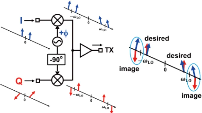
The image signal is basically caused by both amplitude and phase mismatch between the I and Q signals. Figure 10 explains the I/Q up-conversion scheme. I-signal cosωBBt is up-converted by LO signal of cosωLOt, and Q-signal sinωBBtis up-converted by LO signal of sinωLOt. In the combined signal, the desired tone atωLO−ωBBis remained, and the undesired tone atωLO+ωBBis cancelled ideally. If these I/Q signals have amplitude and phase mismatches, the undesired tone will be remained as shown in Fig. 11, called as the image signal. IMRR can be calculated by the follow- ing equation [19].
I MRR=1−2(1+ε) cosθ+(1+ε)2
1+2(1+ε) cosθ+(1+ε)2 ≃ε2+θ2
4 (4)
whereεis voltage amplitude error, andθis phase error in ra- dian. For example, an amplitude error of 0.2 dB and a phase error of 2 degrees results in an IMRR of−34 dB. Figure 12 shows a contour plot of IMRR.
The I/Q amplitude and phase mismatches are caused by I/Q building blocks. The phase mismatch is basically caused by a mismatch in quadrature signals in LO generation, and it is a bit degraded by amplifiers. The amplitude mismatch is degraded by mixers and amplifiers as in Fig. 8. In addition, differential mismatches in mixer and LO generate the LO
Fig. 8 I/Q mismatch in direct-conversion transceiver.
Fig. 9 Image Rejection Ratio and LO feedthrough.
Fig. 10 Up-conversion with I/Q mismatch.
feedthrough even by a double-balanced mixer.
Figure 13 shows an I/Q mismatch calibration technique using a detector [17]. The detector is used for power detec- tion by a second-order distortion. As explained in Fig. 11, the output spectrum consists of the desired (ωLO−ωBB), LO feedthrough (ωLO), image (ωLO+ωBB) tones. The detec-
Fig. 11 Up-converted and combined I/Q signal with I/Q mismatch.
Fig. 12 Image rejection ratio.
tor down-converts these tones, and the largest desired tone works as a LO signal (ωLO−ωBB). The LO feedthrough (LOFT) and image tones are down-converted at ωBB and 2ωBB, respectively.
The receiver building blocks are re-used for analyzing the down-converted tones. Fortunately, the required band- width and resolution coincide with the receiver specifica- tion in a symmetric-rate wireless system such as TDD. Fig- ure 14 shows an example implementation of TX loop-back calibration [17]. The down-converted tones by the detec- tor are digitized through the VGA, LPF, and ADC path, and then DFT is applied to analyze each signal strength. The down-converted LOFT and image signals are used for the TX I/Q mismatch calibration. Usually, the mismatch is com- pensated by a TX filter in the digital baseband. Accurate amplitude and phase compensation can be possible up to the resolution of DAC. Sometimes, the analog calibration is applied [4], [7]. For example, in case of millimeter-wave transceiver, the sampling rate becomes 3.52 GS/s and it be- comes difficult to realize a fine TX filter and high-resolution DAC. Thus, the analog calibration becomes power efficient.
In this case, the LOFT is calibrated by DC offset in DAC, the amplitude mismatch is calibrated by RF/BB amplifiers, and the phase mismatch is calibrated by LO [4].
For RX, a loop-back calibration can also be applied as shown in Fig. 15. The TX can be used as a single tone gener- ator, and the digital baseband is also used for analyzing I/Q amplitude/phase mismatches in the receiver side. In case of RX, modulated I/Q signals can also be used for calculating the amplitude and phase mismatches [18], which can be cal-
Fig. 13 TX image calibration.
Fig. 14 I/Q mismatch calibration by loop-back.
Fig. 15 RF loop-back calibration for RX.
culated as follows.
LPF(I2−Q2) ∝ε (5)
LPF(I Q) ∝θ/2 (6)
This receiver calibration can be applied without the loop- back signal. The receiving signal for actual data communi- cation can also be used for realizing a background calibra- tion.
2.5 IM2 Calibration
Linearity is very important performance not only for trans- mitter but also for receiver. A traditional cellular transceiver employs FDD, and the receivers always suffer from TX leakage and interferer through a duplexer. Non-linearities
ous issue in direct-conversion receivers depending on a re- quired specification such as UMTS/LTE receivers. More than 70 dBm IIP2 is required for WCDMA receiver [13], and even a 1% mismatch degrades IIP2 by 20 dB. More than 40 dBm is usually almost impossible without any calibra- tion due to the PVT variation. Mismatch calibration tech- niques for IIP2 improvement have been reported, and an on-chip automatic IIP2 calibration is reported with the mea- sured+90 dBm IIP2, which is realized by 25-% duty-cycle LO injection and threshold adjust, and current-input com- plex direct coupled filter [13].
3. Digital Calibration and Compensation in Frequency Synthesizers
As well as wireless transceiver, many calibration and com- pensation techniques have been developed for frequency synthesizers. Here, some recent techniques will be intro- duced.
The injection-lock technique is very convenient to im- prove circuit peformances in terms of lower power con- sumption, higher frequency operation, higher order multi- plication, etc. The injection lock is commonly used for a frequency divider. Even by a 3-mW ring oscillator, a divide- by-6 frequency division can be achieved up to 30 GHz [20], which is much more advantageous than current-mode logic (CML), true single phase clocking (TSPC), FF-based fre- quency dividers. One of the issues in injection-lock oscil- lators is the limited lock range in frequency. The center of lock range becomes close to a free-running frequency of injection-locked oscillator, so it can be easily calibrated by using a frequency counter [21], [22]. In addition, a frac- tional division ratio can be realized by an injection-locked frequency divider using the gated-injection technique [23], which is used with a lock-range calibration [24], [25]. A frequency multiplication is also important function of the injection-locked oscillators, and injection-locked PLLs us- ing this multiplication capability have been reported and achieve very low jitter and lower power comsumption [26], [27].
Even in the conventional analog PLLs, many calibra- tion and compensation techniques have been used, e.g., automatic frequency control (AFC) for the bank selection of VCO, KVCO linearity calibration, CP linearity calibra- tion/compensation, etc. As a system-level approach, the all- digital PLL (AD-PLL) is a very important revolution [28], [29], and many building blocks can be replaced by a dig- ital version. AD-PLL uses a digital LPF instead of ana-
is also possible. This is very important advantage of AD- PLL.
4. Digitally-synthesizable Analog Circuits
In wireless systems, analog functions have been replaced by digital signal processing as explained in the prior sections.
However, some analog functions still have to be realized in the analog domain because they need analog value process- ing. As explained in Fig. 2, the following circuits cannot be replaced by a pure digital-domain signal processing: data converters such as ADC and DAC, analog-domain ampli- fiers using voltage and current signal information, and clock generators. Even they are supported by digital calibration and compensation, they cannot be digitized.
To enhance the process portability and scalability, a digitally-designed analog circuit can be considered, i.e., synthesizable analog circuits. For a further digitization, some synthesizable analog circuits have been reported such as synthesizable PLL [31], [32] and synthesizable ADC [33].
If an analog circuit can be designed and generated through the digital design flow as shown in Fig. 16, it will obtain the process portability and scalability. Figure 17 ex- plains a detailed example for a synthesizable PLL. Some building blocks, such as DCO, may still need some spe- cial optimization, while they can be described as a HDL netlist. The netlist of analog block can be combined with the other building blocks, which can be implemented as RTL.
From the entire combined netlist in gate-level, a layout can be generated by a commercial place and route tool. In this case, the generated layout will have unbalanced parasitics as shown in Fig. 18, and the parasitic components depend on the place-and-route condition and cannot be estimated accu- rately before the actual layout generation. This layout uncer- tainty causes the mismatch and non-linearity, which results in circuit performance degradation. Fortunately, the layout uncertainty issue can be mitigated by applying the digital calibration and compensation techniques. Thus, a digitally- designed analog circuit will potentially perform well with the calibration and compensation techniques.
For synthesizable analog circuits, some kinds of cir- cuit performances can be well optimized while some kinds will be difficult to achieve a good performance as well as custom-designed circuits. For example, voltage-domain op- eration cannot be well realized by a synthesizable analog circuit. However, a clock generation is not very difficult be- cause it mainly operates in the time domain. To achieve high
Fig. 16 Synthesizable analog circuits ( c⃝IEEE [31]).
Fig. 17 Analog synthesis by digital tools.
Fig. 18 Layout uncertainty.
performance by a synthesizable analog circuit, a synthesis- friendly architecture has to be developed. As an example of synthesis-friendly PLL, an injection-lock-based PLL is introduced below [31], [32].
To realize a synthesizable PLL, each building block also has to be synthesizable. A digitally-controlled varactor can be realized by a NAND gate [31], [32], [34] as shown in Fig. 19, and a digitally-controlled oscillator (DCO) can also be realized by MUXs and the digitally-controlled var- actor [35]. In addition, a phase-interpolator-based oscilla- tor can be employed and synthesized to mitigate the layout uncertainty issue [31], [32], [36]. A stochastic TDC can be synthesizable [37], and TDC-based synthesizable PLLs have also been reported [38]–[40]. The PLLs [39], [40]
still need special custom cells for layout synthesis. At the present implementation, the jitter performance is degraded by the non-linearity of TDC while it can be potentially im- proved by the calibration techniques [30].
The injection-locked architecture is a promising candi- date for high performance PLL [26], [27], and it is also a good candidate of synthesizable PLL [31], [32]. In the con- ventional PLLs including CP-based and TDC-based ones, the frequency and phase are adjusted by a feedback loop.
The feedback loop needs a fine frequency control and fine phase error detection, and the building blocks for the func- tions easily become bulky. On the other hand, in the injection-locked PLL, a feedback control is not required for the phase lock because the phase is aligned by the injec- tion. Thus, no fine phase control is required, and a coarse frequency adjustment can be employed [27]. As shown in
Fig. 19 Standard cell Varactor ( c⃝IEEE [31]).
Fig. 20 Synthesizable IL-PLL ( c⃝IEEE [31]).
Fig. 21 Chip micrograph and performance summary.
Fig. 20, frequency lock and phase lock can be separated by applying a dual-loop architecture [26], [27], which also con- tributes to reducing layout area and power consumption.
In addition, the in-band phase noise does NOT suffer from non-linearities of TDC, DCO and DTC as well as CP noise, [41], [42], which results in drastic improvement in jitter performance. The PLL loop-bandwidth can be much wider than that of conventional PLLs because of less in- band phase noise. For example, the loop-bandwidth is less than 1 MHz in the conventional PLLs, but it can be 16 MHz in the injection-locked PLL even with the same 40-MHz ref- erence clock [32], [42].
As a demonstration of synthesizable PLL, Fig. 21 shows a chip micrograph and a brief performance summary [31], [32], and Fig. 22 shows a performance comparison with the state-of-the-art PLLs. The fully synthesized PLL achieves 1.7 ps RMS jitter while consuming 780µW power,
Fig. 22 Comparison of the state-of-the-art PLLs ( c⃝IEEE [31]).
resulting in a PLL FoM of−236.5 dB/Hz. PLL FoM is de- fined by the following equation.
FoM=10 log10 {(σt
1 s )2 PDC
1 mW }
(7) whereσt is the jitter in RMS, andPDCis the power con- sumption. As compared with the other synthesized PLLs based on the TDC architecture [38]–[40], the synthesized injection-locked PLL can be smaller due to the less neces- sity of a fine frequency and phase tracking.
In Fig. 22, LC-based PLLs perform better FoM but layout area becomes larger. While ring-oscillator-based PLLs has worse jitter performance, they can be small. The injection-locked PLL can be much smaller because build- ing blocks for the fine frequency and phase tracking are not required, and the jitter can be very small due to the injection- lock architecture. This means that a higher performance can be achieved even by a synthesized analog circuit if a synthesis-friendly architecture can be developed such as the injection-locked PLL. This synthesizable PLL can be de- signed through a common digital design flow, which can maximally contribute to the process portability and scala- bility.
5. Conclusion
In this paper, the digital assisted analog and RF circuit tech- niques are reviewed mainly for wireless systems, includ- ing digital assistance and digitization. Digital calibration and compensation techniques for compensating I/Q mis- match, IM2, and LO impairments in cellular, WiFi, and WiGig transceivers are introduced with detailed analysis and circuit implementations. Synthesizable analog circuits are also introduced for showing a future technology direction, which indicate a trend from digitally-assisted analog circuit to digitally-designed analog circuit.
Acknowledgements
This work is partially supported by MIC, SCOPE, MEXT, STARC, STAR, and VDEC in collaboration with Cadence Design Systems, Inc., Synopsys, Inc., Mentor Graphics, Inc., and Agilent Technologies Japan, Ltd.
T. Sato, H. Asada, N. Takayama, S. Ito, W. Chaivipas, R. Minami, T. Yamaguchi, Y. Takeuchi, H. Yamagishi, M. Noda, and A. Matsu- zawa, “A 60-GHz 16QAM/8PSK/QPSK/BPSK direct-conversion transceiver for IEEE802.15.3c,” IEEE J. Solid-State Circuits, vol.46, no.12, pp.2988–3004, Dec. 2011.
[3] K. Okada, K. Kondou, M. Miyahara, M. Shinagawa, H. Asada, R. Minami, T. Yamaguchi, A. Musa, Y. Tsukui, Y. Asakura, S.
Tamonoki, H. Yamagishi, Y. Hino, T. Sato, H. Sakaguchi, N.
Shimasaki, T. Ito, Y. Takeuchi, N. Li, Q. Bu, R. Murakami, K.
Bunsen, K. Matsushita, M. Noda, and A. Matsuzawa, “A full 4- channel 6.3 Gb/s 60 GHz direct-conversion transceiver with low- power analog and digital baseband circuitry,” IEEE International Solid-State Circuits Conference (ISSCC), pp.218–219, Feb. 2012.
[4] K. Okada, K. Kondou, M. Miyahara, M. Shinagawa, H. Asada, R.
Minami, T. Yamaguchi, A. Musa, Y. Tsukui, Y. Asakura, S. Ta- monoki, H. Yamagishi, Y. Hino, T. Sato, H. Sakaguchi, N. Shima- saki, T. Ito, Y. Takeuchi, N. Li, Q. Bu, R. Murakami, K. Bunsen, K. Matsushita, M. Noda, and A. Matsuzawa, “Full four-channel 6.3- Gb/s 60-GHz CMOS Transceiver with low-power analog and dig- ital baseband circuitry,” IEEE J. Solid-State Circuits, vol.48, no.1, pp.46–65, Jan. 2013.
[5] K. Okada, R. Minami, Y. Tsukui, S. Kawai, Y. Seo, S. Sato, S.
Kondo, T. Ueno, Y. Takeuchi, T. Yamaguchi, A. Musa, R. Wu, M. Miyahara, and A. Matsuzawa, “A 64-QAM 60 GHz CMOS transceiver with 4-channel bonding,” IEEE International Solid-State Circuits Conference (ISSCC), pp.346–347, Feb. 2014.
[6] R. Wu, S. Kawai, Y. Seo, K. Kimura, S. Sato, S. Kondo, T. Ueno, N. Fajri, S. Maki, N. Nagashima, Y. Takeuchi, T. Yamaguchi, A.
Musa, M. Miyahara, K. Okada, and A. Matsuzawa, “A HCI-Healing 60 GHz CMOS transceiver,” IEEE International Solid-State Circuits Conference (ISSCC), Feb. 2015.
[7] T. Tsukizawa, N. Shirakata, T. Morita, K. Tanaka, J. Sato, Y.
Morishita, M. Kanemaru, R. Kitamura, T. Shima, T. Nakatani, K.
Miyanaga, T. Urushihara, H. Yoshikawa, T. Sakamoto, H. Moto- zuka, Y. Shirakawa, N. Yosoku, A. Yamamoto, R. Shiozaki, and N.
Saito, “A fully integrated 60 GHz CMOS transceiver chipset based on WiGig/IEEE802.11ad with built-in self-calibration for mobile applications,” IEEE International Solid-State Circuits Conference Dig. Tech. Papers, pp.230–231, Feb. 2013.
[8] O. Momeni, “A 260 GHz amplifier with 9.2 dB gain and−3.9 dBm saturated power in 65 nm CMOS,” IEEE International Solid-State Circuits Conference Dig. Tech. Papers, pp.140–141, Feb. 2013.
[9] B. Razavi, “A 300-GHz fundamental oscillator in 65-nm CMOS technology,” IEEE J. Solid-State Circuits, vol.46, no.4, pp.894–903, Apr. 2011.
[10] O. Momeni and E. Afshari, “High power terahertz and millimeter- wave oscillator design: A systematic approach,” IEEE J. Solid-State Circuits, vol.46, no.3, pp.583–597, Mar. 2011.
[11] H. Sherry, J. Grzyb, and R. Z. Yan, A. Hadi, A. Cathelin, A. Kaiser, and U. Pfeiffer, “A 1 k pixel CMOS camera chip for 25 fps real- time terahertz imaging applications,” IEEE International Solid-State Circuits Conference (ISSCC), pp.252–253, Feb. 2012.
[12] I. Aoki, S. Kee, R. Magoon, R. Aparicio, F. Bohn, J. Zachan, G. Hatcher, D. McClymont, and A. Hajimiri, “A fully integrated quad-band GSM/GPRS CMOS power amplifier,” IEEE International Solid-State Circuits Conference (ISSCC), pp.570–571, Feb. 2008.
[13] D. Kaczman, M. Shah, M. Alam, M. Rachedine, D. Cashen, L.
Han, and A. Raghavan, “A single-chip 10-band WCDMA/HSDPA 4-band GSM/EDGE SAW-less CMOS receiver with DigRF 3G in- terface and+90 dBm IIP2,” IEEE J. Solid-State Circuits, vol.44, no.3, pp.718–739, Mar. 2009.
[14] H. Suzuki, Y. Yamao, and H. Kikuchi, “A single-chip MSK coher- ent demodulator for mobile radio transmission,” IEEE Trans. Veh.
Technol., vol.34, no.4, pp.157–168, Nov. 1985.
[15] F. M. Gardner, “Interpolation in digital modems. I: Fundamentals,”
IEEE Trans. Commun., vol.41, no.3, pp.501–507, Mar. 1993.
[16] A. Jerng, “Digital calibration for RF transceivers,” IEEE Interna- tional Solid-State Circuits Conference (ISSCC), Tutorial 9, Feb.
2012.
[17] I. Vassiliou, K. Vavelidis, T. Georgantas, S. Plevridis, N. Haral- abidis, G. Kamoulakos, C. Kapnistis, S. Kavadias, Y. Kokolakis, P. Merakos, J. C. Rudell, A. Yamanaka, S. Bouras, and I. Bouras,
“A single-chip digitally calibrated 5.15–5.825-GHz 0.18-µm CMOS transceiver for 802.11a wireless LAN,” IEEE J. Solid-State Circuits, vol.38, no.12, pp.2221–2231, Dec. 2003.
[18] S. Lerstaveesin and B.-S. Song, “A complex image rejection circuit with sign detection only,” IEEE J. Solid-State Circuits, vol.41, no.12, pp.2693–2702, Dec. 2006.
[19] B. Razavi, “Design considerations for direct-conversion receivers,”
IEEE Trans. Circuits Syst. II, Analog Digit. Signal Process., vol.44, no.6, pp.428–435, June 1997.
[20] T. Siriburanon, W. Deng, A. Musa, K. Okada, and A. Mat- suzawa, “A 13.2% locking-range divide-by-6, 3.1mW, ILFD using even-harmonic-enhanced direct injection technique for millimeter- wave PLLs,” IEEE European Solid-State Circuits Conference (ESS- CIRC), pp.403–406, Sept. 2013.
[21] S. Pellerano, R. Mukhopadhyay, A. Ravi, J. Laskar, and Y. Palaskas,
“A 39.1-to-41.6 GHz DS fractional-N frequency synthesizer in 90- nm CMOS,” IEEE International Solid-State Circuits Conference (ISSCC), pp.484–485, Feb. 2008.
[22] T. Shima, J. Sato, K. Mizuno, and K. Takinami, “A 60 GHz CMOS PLL synthesizer using a wideband injection-locked frequency di- vider with fast calibration technique,” Asia-Pacific Microwave Con- ference, pp.1530–1533, Dec. 2011.
[23] S. Hara, K. Okada, and A. Matsuzawa, “10 MHz to 7 GHz quadra- ture signal generation using a divide-by−4/3, −3/2, −5/3, −2,
−5/2,−3,−4, and−5 injection-locked frequency divider,” IEEE Symposium on VLSI Circuits, pp.51–52, June 2010.
[24] W. Deng, A. Musa, K. Okada, and A. Matsuzawa, “A 0.38 mm2, 10 MHz–6.6 GHz quadrature frequency synthesizer using fractional- N injection-locked technique,” IEEE Asian Solid-State Circuits Conference (A-SSCC), pp.353–356, Nov. 2012.
[25] W. Deng, S. Hara, A. Musa, K. Okada, and A. Matsuzawa, “A compact and low-power fractionally injection-locked quadrature fre- quency synthesizer using a self-synchronized gating injection tech- nique for software-defined radios,” IEEE J. Solid-State Circuits, vol.49, no.9, pp.1984–1994, Sept. 2014.
[26] W. Deng, A. Musa, T. Siriburanon, M. Miyahara, K. Okada, and A. Matsuzawa, “A 0.022 mm2970µW dual-loop injection-locked PLL with−243 dB FOM using synthesizable all-digital PVT cali- bration circuits,” IEEE International Solid-State Circuits Conference (ISSCC), pp.248–249, Feb. 2013.
[27] A. Musa, W. Deng, T. Siriburanon, M. Miyahara, K. Okada, and A.
Matsuzawa, “A compact, low power and low jitter dual-loop injec- tion locked PLL using all-digital PVT calibration,” IEEE J. Solid- State Circuits, vol.49, no.1, pp.50–60, Jan. 2014.
[28] R. B. Staszewski, K. Muhammad, D. Leipold, C.-M. Hung, Y.-C.
Ho, J. L. Wallberg, C. Fernando, K. Maggio, R. Staszewski, T. Jung, J. Koh, S. John, I. Y. Deng, and V. Sarda, O. Moreira-Tamayo, V.
Mayega, R. Katz, O. Friedman, O. E. Eliezer, E. de-Obaldia, and P. T. Balsara, “All-digital TX frequency synthesizer and discrete- time receiver for Bluetooth radio in 130-nm CMOS,” IEEE J. Solid- State Circuits, vol.39, no.12, pp.2278–2291, Dec. 2004.
[29] R. B. Staszewski, J. L. Wallberg, S. Rezeq, C.-M. Hung, O. E.
Eliezer, S. K. Vemulapalli, C. Fernando, K. Maggio, R. Staszewski, N. Barton, M.-C. Lee, P. Cruise, M. Entezari, K. Muhammad, and D.
Leipold, “All-digital PLL and transmitter for mobile phones,” IEEE J. Solid-State Circuits, vol.40, no.12, pp.2469–2482, Dec. 2005.
[30] S. Levantino, G. Marzin, and C. Samori, “An adaptive pre-distortion technique to mitigate the DTC nonlinearity in digital PLLs,” IEEE J. Solid-State Circuits, vol.49, no.8, pp.1762–1772, Aug. 2014.
[31] W. Deng, A. Musa, T. Siriburanon, M. Miyahara, K. Okada, and A.
Matsuzawa, “A 0.0066-mm2780-µW fully synthesizable PLL with a current output DAC and an interpolative-phase coupled oscillator using edge injection technique,” IEEE International Solid-State Cir- cuits Conference (ISSCC), pp.266–267, Feb. 2014.
[32] W. Deng, D. Yang, T. Ueno, T. Siriburanon, S. Kondo, K. Okada, and A. Matsuzawa, “A fully synthesizable all-digital PLL with in- terpolative phase coupled oscillator, current-output DAC, and fine- resolution digital varactor using gated edge injection technique,”
IEEE J. Solid-State Circuits, vol.50, no.1, pp.68–80, Jan. 2015.
[33] S. Weaver, B. Hershberg, and U.-K. Moon, “Digitally synthesized stochastic flash ADC using only standard digital cells,” IEEE Trans.
Circuits Syst. I, Reg. Papers, vol.61, no.1, pp.84–91, Jan. 2014.
[34] P.-L. Chen, C.-C. Chung, and C.-Y. Lee, “A portable digitally con- trolled oscillator using novel varactors,” IEEE Trans. Circuits Syst.
II, Exp. Briefs, vol.52, no.5, pp.233–237, May 2005.
[35] D. Sheng, C. C. Chung, and C. Y. Lee, “An ultra-low-power and portable digitally controlled oscillator for SoC applications,” IEEE Trans. Circuits Syst. II, Exp. Briefs, vol.54, no.11, pp.954–958, Nov.
2007.
[36] A. Matsumoto, S. Sakiyama, Y. Tokunaga, T. Morie, and S. Dosho,
“A design method and developments of a low-power and high- resolution multiphase generation system,” IEEE J. Solid-State Cir- cuits, vol.43, no.4, pp.831–843, Apr. 2008.
[37] P. M. Levine and G. W. Roberts, “A high-resolution flash time-to- digital converter and calibration scheme,” IEEE International Test Conference, pp.1148–1157, Oct. 2004.
[38] Y. Park and D. D. Wentzloff, “An all-digital PLL synthesized from a digital standard cell library in 65 nm CMOS,” IEEE Custom Inte- grated Circuits Conference (CICC), Oct. 2011.
[39] W. Kim, J. Park, J. Kim, T. Kim, H. Park, and D. Jeong, “A 0.032 mm23.1 mW synthesized pixel clock generator with 30 psrms inte- grated jitter and 10-to-630 MHz DCO Tuning Range,” IEEE Inter- national Solid-State Circuits Conference (ISSCC), pp.250–251, Feb.
2013.
[40] M. Faisal and D. D. Wentzloff, “An automatically placed-and-routed ADPLL for the MedRadio band using PWM to enhance DCO Res- olution,” IEEE Radio Frequency Integrated Circuits Symposium, pp.115–118, June 2013.
[41] S. Ye, L. Jansson, and I. Galton, “A multiple-crystal interface PLL with VCO realignment to reduce phase noise,” IEEE J. Solid-State Circuits, vol.37, no.12, pp.1795–1803, Dec. 2002.
[42] N. D. Dalt, “An analysis of phase noise in realigned VCOs,” IEEE Trans. Circuits Syst. II, Exp. Briefs, vol.61, no.3, pp.143–147, Mar.
2014.
has been an Associate Professor at Department of Physical Electronics, Tokyo Institute of Technology, Tokyo, Japan. He has authored or co-authored more than 300 journal and conference papers.
His current research interests include reconfigurable RF CMOS circuits for millimeter-wave CMOS wireless frontends, cognitive radios, and low- voltage RF circuits Dr. Okada is a member of IEEE, the Institute of Elec- tronics, Information and Communication Engineers (IEICE), the Informa- tion Processing Society of Japan (IPSJ), and the Japan Society of Applied Physics (JSAP). He received the Ericsson Young Scientist Award in 2004, the A-SSCC Outstanding Design Award in 2006 and 2011, the ASP-DAC Special Feature Award in 2011 and Best Design Award in 2014, JSPS Prize in 2014 and 35 international and domestic awards. He is a member of the ISSCC Technical Program Committee.

![Fig. 20 Synthesizable IL-PLL ( c ⃝ IEEE [31]).](https://thumb-ap.123doks.com/thumbv2/123deta/5625374.1500150/7.892.100.399.118.574/fig-synthesizable-il-pll-c-ieee.webp)
![Fig. 22 Comparison of the state-of-the-art PLLs ( c ⃝ IEEE [31]).](https://thumb-ap.123doks.com/thumbv2/123deta/5625374.1500150/8.892.104.399.117.306/fig-comparison-state-art-plls-c-ieee.webp)
