Kazuhiko ENDO†a),Nonmember, Shin-ichi OUCHI†,Member, Takashi MATSUKAWA†, Yongxun LIU†, andMeishoku MASAHARA†,Nonmembers
SUMMARY Multi-Gate device technology is the promising candidate for the enhancement of device characteristics of the scaled MOSFETs.
Moreover, independent-double-gate devices have been proposed to achieve flexibleVthadjustment. It is revealed that the SRAM noise margins have been increased by introducing the independent-double-gate FinFET.
key words: multi-gate devices, FinFET, SRAM, noise margin
1. Introduction
Due to the rapid reduction of the feature size of comple- mentary metal oxide semiconductor (CMOS) devices, de- vice technology is facing several difficulties. Short channel effects (SCEs) such as the threshold voltage roll-offand the sub-threshold slope (s-slope) degradation caused by the re- duced drivability of the gate electrode cause significant in- crease in power consumption and become a limiting factor in MOS devices. In addition, variability of the CMOS de- vice is increasing and reduces the yield of the CMOS cir- cuit. Especially, the SRAM cell uses the smallest transis- tor to achieve high density integration and the yield of the SRAM cell is rapidly decreasing. Thus, reduction of the SCE, standby power consumption, and variability is becom- ing the most important issues in CMOS devices. In this re- port, we review the effectiveness of introducing multi-gate device especially independent gate device in the SRAM cell.
2. Advantage of the Multi-Gate Device
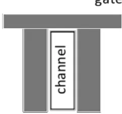
To enhance the short-channel effects immunity and re- duce the leakage current of the scaled MOSFET, double- gate (DG) device technology has firstly been invented by Sekigawa et al. in 1980 [1]. The channel region of the de- vice is sandwiched by a double-gate. The double-gate struc- ture increases the electrostatic controllability and effectively controls the channel potential and reduces the short channel effects. Figure 1 shows an original concept of the double- gate devices. They named this device as a XMOSFET and they improved the characteristics by using a vertical chan- nel as shown in Fig. 2 [2], which is known as a FinFET.
They succeeded in fabricating the double-gate devices and showed the superiority of the device characteristics in 1985 [3].
Manuscript received August 10, 2012.
†The authors are with National Institute of Advanced Industrial Science and Technology (AIST), Tsukuba-shi, 305-8568 Japan.
a) E-mail: [email protected] DOI: 10.1587/transele.E96.C.413
Fig. 1 A schematic illustration of the original invention of the double- gate device.
Fig. 2 A schematic illustration of the vertical channel double gate device.
In 1989, Hisamoto et al. reported a fully depleted lean- channel transistor (DELTA) SOI MOSFET using the vertical channel and the double-gate configuration [4]. By using this configuration, the self-aliened double-gate can easily be fab- ricated. In 1998, he and his coauthors also reported a folded channel MOSFET [5] with the vertical ultra-thin channel and the double-gate. They called the folded vertical chan- nel as a “Fin”, and which become common for representing the vertical silicon ultra thin channel. Currently, the Fin- FET with the double-gate and the upstanding “Fin” becomes common MOSFET thanks to its high process compatibility with the conventional MOSFET.
Superiority of the double-gate device is also predicted by the calculation. Sub-threshold swing degradation and other short channel effects such as the reduction of theVth are caused by the encroachment of electric field lines from the source to the drain. Yan et al. introduced a natural length that controls the spread of the electric filed in the channel di- rection [6]. The natural length of the single gate MOSFET is described by (1) while that of the double gate device is described by (1).
λ1 = εS i
εoxtoxtsi (1)
Copyright c2013 The Institute of Electronics, Information and Communication Engineers
Fig. 3 A schematic illustration of the variation sources in the FinFET.
λ2= εS i
2εox
toxtsi (2)
It is reported that the effective gate length of a MOS- FET device must be larger than 5 to 10 times the natural length to prevent short channel effects and produce a reason- able sub-threshold behavior [6]. According to (1) and (2), the natural length of the double-gate device is much smaller than that of the single gate device and therefore the double gate device effectively suppress the short channel effects. In addition, increasing the number of the gate electrodes fur- ther suppresses the short channel effects and the triple gate device or eventual surrounding gate device have also been proposed as one of the multi-gate devices [7], [8].
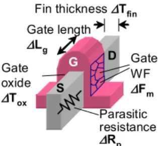
In addition to the better short channel control, the multi-gate device can reduce the variability in device char- acteristics. Due to the better electrostatic controllability of the channel potential, the multi-gate device allow the use of the intrinsic channel with no dopant and the non-doped channel effectively suppress the random dopant fluctuation which is the main cause of the variation in the current bulk MOSFETs. The variability issues are summarized in Fig. 3.
The variability is caused by the dimension variations such as gate length, channel thickness, and gate oxide thickness [9], [10]. Also, it is caused by the random dopant fluctuation in the channel [11], [12], and work-function variation due to the granularity of the gate-electrode [13]–[16]. The metal gate (MG) electrode has become a primary technology for the advanced CMOS application to suppress gate depletion, control the threshold voltage (Vth), and overcome incompat- ibility of the poly-silicon gate to high-k materials. However, using the MG introduces a new variation due to the depen- dency of the work function (WF) on the orientation of metal grains.
The variability of the MOSFET is characterized by the Pelgrom plot [17]. In this plot, standard deviation of the threshold voltage (σVth) is plotted as a function of the square root of the inverse channel area 1/(LGxWG) whereLGis the gate length andWGis the gate width since thesVthis repre- sented by (3).
σVth2 = Avt
LW +B (3)
The slope of the Pelgrom plot called Avt represents the variation of the MOSFET in the certain device fabrication technology. Figure 4 shows the benchmark of the Avt. The
Fig. 4 A benchmark of the Avt value.
Fig. 5 Ion-Ioffplot of the scaled transistors; (a) nFET, (b) pPET.
multi-gate device such as the FinFET and fully depleted SOI (FDSOI) devices provide smaller Avt due to the intrinsic channel.
If we use the typical (100) Si wafer, the vertical channel orientation is 110. The previous literature indicates that the hole mobility on the (110) surface is higher than that of the (100) surface [18]. On the other hand, the electron mo- bility on the (110) channel degrades. However, this degrada- tion is not an issue thanks to the recent channel engineering technology. The electron and the hole mobility on the (110) channel can be effectively improved by adding stress by the stressor materials [19]. Figure 5 shows the Ion/Ioff plot of the FinFET. Thanks to the excellent high-k/metal-gate gate stack fabrication technology and the excellent channel engi- neering to introduce stress, the superior on-current (Ion) with the reasonable off-current (Ioff) is realized.
3. The FinFET SRAM Cell
3.1 Advantage of the FinFET SRAM Cell
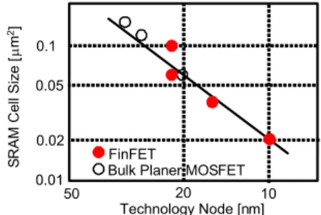
Recently, scaled SRAMs are confronted with a severe degra- dation in the cell stability which affects the yield of LSIs because the SRAM cells use the smallest transistors and oc- cupy a considerable part of the LSI. Due to these advantages of the double-gate devices, many studies have focused on the FinFET SRAM cells to overcome the rapid decrease in the conventional SRAM performance [19]–[23]. The influ- ence of FinFET variability on the SRAM performance has also been studied [13], [24]. Figure 6 summarizes the re- ported cell size for the scaled FinFET SRAM. Drastic re-
Fig. 6 The reported SRAM cell size as a function of the technology node.
Fig. 7 Schematic illustrations of the FinFET; (a) common DG FinFET, (b) independent DG FinFET.
Fig. 8 ID-VGcharacteristics of the FinFETs; (a) nMOS, (b) pMOS.
duction of the SRAM cell size can be realized thanks to the excellent SCE immunity of the FinFET. However, the SRAM operation is not free from the trade-offrelationship between the read and the write margins even for the Fin- FET SRAMs. Thus, a new method to enhance the stability is required. This will be realized by dynamically controlling the threshold voltage (Vth) of the pass gate. The following section describes new SRAM cells with the independent- double-gate devices.
3.2 Independent-DG FinFET SRAM Cell
In 2004, Liu proposed aVthcontrollable four terminal (4T) FinFET with the independent double-gate (DG) by separat- ing the connection between the common DG [25]. One gate electrode can be used as a signaling gate and the other gate can be used as aVthcontrol gate as schematically shown in Fig. 7(b). The chemical mechanical polishing process and the etching based process has been carried out for the gate separation [25], [26]. Figure 8 shows the current-voltage characteristics of the conventional common-DG (CDG) Fin- FET and the independent-DG (IDG) FinFET with various biasing condition for theVthcontrol gate. Flexible control of
Fig. 9 Schematic illustrations of the SRAM cell.
Fig. 10 Proposed layouts for the SRAM cell; (a) bulk planer, (b) CDG- FinFET, (c) Flex-Vth, (d) Flex-PG.
theVthof the FinFET by the control gate can be clearly seen.
It should be noted that the values ofVthshift rateγdefined by−ΔVth/ΔVG2is higher than that obtained by the conven- tional body-bias control of the planar MOSFETs [27].
Figure 9 shows the schematic topologies of the Fin- FET SRAM cells using the IDG-FinFET. One is a flexible- Vth (Flex-Vth) SRAM cell (Fig. 9(a)) [28] and the other is a flexible pass-gate (Flex-PG) SRAM cell (Fig. 9(b)) [29], [30]. In the Flex-Vth cell, all the transistors in the cell are composed by the IDG-FinFET. The Vth of the all transis- tor can be controlled by the external bias to theVth-control- gate (VG2NandVG2P). For the Flex-PG cell, IDG-FinFETs are used only for the PG and the other transistors are com- posed by the common-DG FinFET. The Ion ratio of the pull down to the pass gate which corresponds to theβ-ratio is thus flexibly changed. TheVG2lines to controlVthare im- plemented parallel with the bit lines and theVthcontrol is executed column-by-column. In the read operation, the cor- respondingβ-ratio is increased by raising theVthof the pass gates. On the other hand, in the write operation, the write margin is enhanced by lowering the Vth of the pass gates.
Consequently, theVthflexibility in the pass gate makes the SRAM cell free from the trade-offrelationship between the read and the write margins. Although additional contact ar- eas are needed for the IDG-FinFET cells, total cell areas are comparable to the bulk cell as shown in Fig. 10. It should be noted that, for the Flex-Vthand Flex-PG SRAM, additional Vth-control lines are required to supply the bias voltage to the accessed cell.
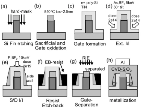
Fig. 11 Schematic device fabrication processes for the FinFET.
3.3 Fabrication of the SRAM Cell
We used lightly dope p-type (100)-oriented silicon-on- insulator (SOI) wafers; thus, the channel-orientations of the fabricated FinFETs were (110). Schematic device fabrica- tion processes are shown in Fig. 11. A 50-nm-thick non- doped silicate glass (NSG) layer and the electron beam (EB) resist masks were formed to make hard masks on the wafer.
To fabricate vertical Si-Fins, the SOI layer was etched by a conventional reactive ion etching (RIE) using a Cl2 induc- tively coupled plasma (ICP) as shown in Fig. 11(a). After the Si-Fin etching, a 2.5-nm-thick gate-oxide was formed at 850◦C followed by the TiN and n+polycrystalline-Si (poly- Si) gate formation using EB lithography and the RIE. Af- ter the gate electrode was formed, a shallow implantation into the extension of the source/drain (S/D) was performed.
To distribute impurity atoms (BF2 for pMOS and As for nMOS) uniformly into the vertical channel, 60-degree tilted implantation was carried out at an acceleration energy of 5 keV and a dose of 2×1014cm−2 in each side [31]. A 1-nm-thick screening oxide was used to suppress the signif- icant dopant loss [32], [33]. A S/D implantation was per- formed at an acceleration energy of 10 keV and a dose of 2×1015cm−2after a 50-nm-thick gate-sidewall was formed by using CVD grown SiO2. The acceleration energy was set to 10 keV to preserve the seed-crystal layer for the recrys- talline annealing.
Then, the poly-Si gate for the IDG-FinFET was sepa- rated by using a newly developed resist etch-back process [26] whereas the CDG-FinFET region was protected by a thicker photo-resist. Due to the three-dimensionally shaped Si-Fin, the thickness of the spin-coated EB resist was thin- ner at the top of the Si-Fin than that at the other planar por- tion. Consequently, the poly-Si gate at the top of the Si- Fin was revealed by the partial ashing of the EB resist as shown in Fig. 11(f). After the poly-Si gate was revealed by thinning the EB resist, the poly-Si gate was separated us- ing RIE with HBr based chemistry and the poly-Si gate over the Si-Fin connected to the each side of the gate was com- pletely removed. Finally, the S/D was activated at 830◦C for 2 seconds and the devices were sintered at 450◦C in 3% H2
Fig. 12 A cross sectional TEM image of the FinFET (a) and a plane SEM image (b) of the SRAM cell.
Fig. 13 Experimental butterfly curves and short circuit currents of the Flex-Vth cell as a function of various biasing conditions.
ambient after the metallization. Figure 12 shows the cross sectional transmission electron microscope (TEM) image of the fabricated FinFET and the plane scanning electron mi- croscope (SEM) image of the SRAM cell.
3.4 Characteristics of the SRAM Cell
The concept of the new SRAM cell with the IDG-FinFET is to dynamically reduce the SRAM leakage current using the Flex-Vth cell. Figure 13 shows the experimental butterfly curves and short circuit currents with various biasing con- ditions. By applying opposite bias voltages to the pMOS and nMOS IDG-FinFETs (VG2N andVG2P), the real values ofVthcan be tuned keeping the symmetry ofVth. Thus, the stand-by leakage current and the short circuit current of the cell are dynamically controlled maintaining the same noise margin. The lower stand-by current is appropriate for the stand-by cell, and the high power operation is applicable for the accessed cell to maintain access speed.
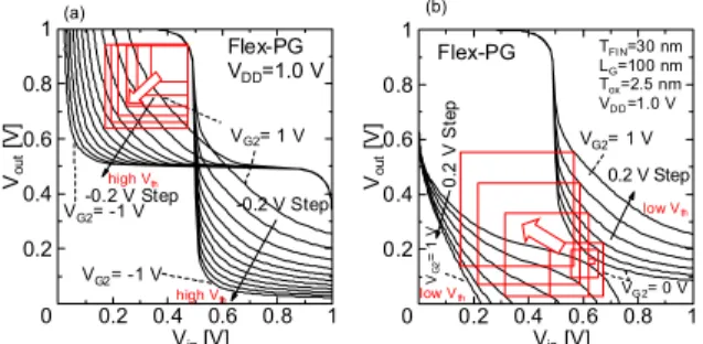
The next concept is to dynamically control the PG to enhance noise margins. A great enhancement of the read margin is experimentally confirmed by lowering theVG2as shown in Fig. 14(a). In addition, by increasing theVG2for the PG, the highest write margin can be obtained as shown in Fig. 14(b). To clarify the effects of theVG2, the read and write margins are summarized as a function of the VG2as shown in Fig. 15. During the read operation, applying the VG2of 0 V enhances the read margin, while theVG2of 1 V during the write operation increases the write margin. Thus, enhancement of both the read and write margins by control- ling the appropriateVG2is clearly confirmed. These experi-
Fig. 14 Experimental butterfly curves for the read margin (a) and write margin (b) evaluation with variousVG2conditions.
Fig. 15 Experimental noise margins as a function of the VG2for the pass gate.
Fig. 16 Comparison of the read margin as a function of the supply voltage.
mental results approve the effectiveness of the Flex-PG cell for suppressing the trade-offrelationship of read and write margins. Figure 16 summarizes theVDDdependence of the read margins for the evaluated SRAM cells. The read mar- gins of the IDG-FinFET SRAM cells are much higher than that of the standard FinFET SRAM cell.
4. Variability Issues
4.1 Variability Issues in the FinFET
As mentioned in the introduction, the FinFET uses the non- dope channel and thus the random dopatnt fluctuation can be avoided. However, variability of the FinFET occurs and its origin has not been understood well. Possible varia-
Fig. 17 ID-VGcharacteristics of the TiN Metal-Gate FinFET.
Fig. 18 Pelgrom plot of the FinFET.
tion sources are fluctuations of the gate-length (ΔLG), the fin-width (ΔTFin), the oxide thickness (ΔTox), the line edge roughness of fin and gate electrodes, random dopant, and work-function variation as already shown in Fig. 3. Re- cently, a mid-gap TiN MG is commonly used to adjust the Vthof the CMOS FinFET with an undoped channel. There- fore, it is valuable to comprehensively analyze variability in the TiN MG FinFET. In addition to the Vth variation, the on-current variation (ΔIon) will also affect the circuit perfor- mance. TheΔIonis caused not only by theΔVth, but also by the parasitic resistance variation (ΔRp) and theΔTox. In this paper, we thoroughly investigate variability in the TiN MG FinFET.
Figure 17 shows typical ID-VG characteristics of the fabricated FinFETs. Although variation of characteristics exists, symmetrical characteristics of pMOS and nMOS Fin- FETs are realized thanks to the mid-gap TiN MG. A con- siderableVthvariation is clearly seen even for the undoped channel FinFET. Figure 18 shows the Pelgrom plot. It ex- hibits a linear relationship indicating that the variation in- creases with scaling of gate area. It is noteworthy that the slopes of the Pelgrom plot (Avt values) of undoped pMOS and nMOS FinFETs are almost the same as shown in Fig. 18. This is much different from those in the case of the doped-channel in which the channel doping induces a larger Vth variation for the nMOS than that of the pMOS transistor due to the transient enhanced diffusion (TED) of boron in the nMOS transistor [34], [35].
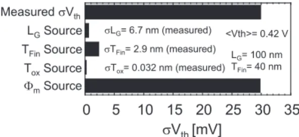
To understand the origin of theVthvariation in the TiN MG FinFET, we experimentally evaluate the effect of the ΔLG, ΔTFin, and ΔTox to the Vth variation by measuring
Fig. 19 Vthvariations due to theΔLGΔTFinandΔTox. These values are small indicating that the dominantVthvariation source is the WFV.
the standard deviation of these values. The effect of these components can be evaluated since the overallVthvariation (σVth) is divided by its components as indicate by the error propagation law (4).
σVt2 = ∂Vt
∂LG
σLG
2
+ ∂Vt
∂TFin
σTFin
2
+ ∂Vt
∂Tox
σTox
2
+ ∂Vt
∂Φm
σΦm
2
(4) The standard deviations of the dimension variation sources such as theΔLGandΔTFinwere measured by count- ing the statistical distribution of the size using a scanning electron microscope (SEM). The same chip is used after the electrical measurements. TheΔToxvariation was measured by ellipsometry using (110) oriented test wafers which have the same orientation with the side-wall channel of the Fin- FET. Partial derivatives in (4) were evaluated by measuring the dependence of theVthwith theLG,TFin, andTox. The ex- perimental results of these contributions are summarized in Fig. 19. It is revealed that theΔLG,ΔTFin, andΔToxcontri- butions to theVthvariation are insignificant since their stan- dard deviations and partial derivatives are small. Thus, it is concluded that the main variation source of the TiN MG FinFET is the work function variation (WFV) of the TiN.
The observedσΦm of 30 mV is almost the same value with the previous reports [14], [15]. The possible explanation of the WFV is an over 200 mV work function difference be- tween (100) and (111) oriented grains of TiN and there is also an additional WFV due to the composition or nitrogen concentration of the TiN [36]. Although the grain size of the TiN at side wall of the fin is different from the planar portion, the transmission electron microscope (TEM) obser- vation of the planar test structure reveals that the grain size of the sputter-deposited TiN is around 20 nm.
Figure 20 shows statisticalIonvariation of the 100-nm- longLGFinFETs extracted at a constantVG(VG=1 V) and at a constant overdrive (VG=Vth+0.65 V). Note that theΔVth
contribution to theΔIonis cancelled out in the constant over- drive case. It is clear form Fig. 20 that the variation of the Ion is much higher for the constantVGcase. This strongly support that theΔVthis the major source of theIonvariation.
The smallIonvariation in the constant overdrive case is due to the smallμ,Rp, andTox variation. This result indicates that if we can reduce the WFV of the TiN MG FinFET, the circuit performance can be improved. A selection of the gate
Fig. 20 Statistical ion variation of the 100-nm-long LG FinFETs ex- tracted at a constant VG (VG = 1 V) and at a constant overdrive (VG=Vth+0.65 V).
Fig. 21 Experimental butterfly curves of the common-DG FinFET SRAM cell.
material and an optimization of the gate formation process are therefore the key for improving the MG FinFET charac- teristics.
4.2 SRAM Variation
TheseVthandIonvariations will directly cause the variation in the SRAM performance. Fortunately, IDG-FinFET tech- nology effectively controls of theVthand thus can be used for the compensation of variability. In this section, variabil- ity of the CDG SRAM cell is compared with the Flex-PG cell. Moreover, experimental demonstration of the SRAM cell stability enhancement is shown using the IDG-FinFETs with the individualVth controlling for the PG and the flip- flop (FF).
Experimental butterfly curves of the conventional CDG cell is shown in Fig. 21. The conventional CDG cell suffers from a marginal SNM due to the variation of the character- istics of the FinFET. To understand the appearance of the irregular curve in Fig. 21, characteristics of each transistor in the exactly same cell are measured. It is revealed that the irregular curves are due to the systematic variation in each FinFET. In this case, all the threshold voltages of the PG, PU, and PD are shifted negatively at the same time. This is explained by the WF lowering due to the composition or the thickness variation of the TiN gate. In addition, by correlat- ing other butterfly curves with the IV characteristics of the FinFETs in each cell, it is concluded that the variation of the SRAM cell is due to theVthvariation caused by the WFV.
On the other hand, Fig. 22 shows the characteristics of the Flex-PG cell. The fixed bias for all the PG in the ac-
Fig. 22 Experimental butterfly curves of the Flex-PG FinFET SRAM cell.
Fig. 23 Noise margin distributions of the CDG and Flex-PG cell during 1 V and 0.5 V operation.
cessed column is applied to reduce the drivability. In this case,VG2is fixed at half of theVDD. TheVth variation of the IDG-FinFET still exists, however, a significant enhance- ment of the SNM is clearly shown and an effect ofVthvaria- tion is decreased. The typical read current of the CDG cell is 11μA, whereas that of the Flex-PG cell is 5μA with the bias voltage (VG2) of 0.5 V. Thus, there is a trade-offbetween the SNM enhancement and the read current. While in a writ- ing operation, theVth of PG can be lowered by the control terminal and the writing time can be shortened compared to the CDG cell.
Figure 23 shows the probability distribution of the noise margins. A 1.7x enhancement in the SNM is suc- cessfully demonstrated. It is also revealed that the statistical distributions of the noise margins of the CDG and Flex-PG cells are similar regardless of the operation voltage. This in- dicate that the average value of the SNM decreases with the sameσ(SNM) when the VDD decreases.
4.3 Compensation of Variability in the SRAM Cell To demonstrate how to cancel the SRAM variation after the fabrication, the experimental cell with the customVth tun- ing for the PG and the flip-flop (FF) for each cell is inves- tigated. Firstly, the FF operation is harmonized so that the logical threshold of the FF keeps 0.5 V by controlling the bias for the second gate in each transistor. However, the variation due to the PG is still present. Secondary, the PG is harmonized by applying the bias voltage so that the Vo
Fig. 24 Experimental reduction of the variation by tuning (a) the bias voltage for the flip-flop, and (b) both the bias voltages for the flip-flop and the pass-gate.
Fig. 25 Butterfly curves for the FinFET SRAM cells. Large variation of the SNM exists. SNMLandSNMRare defined depending on the two different memory states. The squares in the figure show worst caseSNML
andSNMR.
keeps constant as shown in Fig. 24(b). As a results, SRAM characteristics become completely healthy and the smallest σ(SNM) is clearly demonstrated. These results indicate that not only the characteristics of the FF but also that of the PG needs to be independently harmonized to achieve the varia- tion tolerant SRAM cell operation. This method cannot be directly applicable to the large scale of SRAM matrix, how- ever, the area based FF/PG tuning with a reasonable number of control lines to decrease the systematicVthvariation may be a possible solution for the SRAM matrix.
4.4 Correlation of Variability in the SRAM Cell
In the previous section, the characteristics of the SRAM cell are harmonized by tuning the characteristic of each FinFET.
However, it is not clear how the variation of the each transis- tor affects the variation on the SNM. In this study, to analyze the effect of theVthvariation on the SNM in detail, we define theSNML andSNMR representing the static noise margins with the different memory state of the storage node L and R as shown in Fig. 25. Usually, the SNM of the SRAM cell is defined by taking the minimum between the SNML and the SNMR. In this study, the correlation between the variation in each transistor and the SNM is analyzed by determining the Vthof the pull-up (PU), pull-down (PD), and pass-gate (PG) transistors and theSNMLand theSNMRof each SRAM cell.
Figure 26 shows the effects of theVthof each transistor
Fig. 26 Relationship between the SNMs and theVthof thePDL(a),PUL
(b), andPGL(c).
on theSNMLandSNMR. In this analysis, we focus on the transistors in node L. We reveal that theSNMLhas a positive correlation with theVth of thePDLandPUL. On the other hand, theSNMRhas a negative correlation with thePDLand a positive correlation with thePGL. No correlation is found between thePUL and theSNMRand between thePGL and theSNML. Thus, theVth of each transistor correlates with the SNMs and the correlation is strongly dependent on the SRAM memory state. If we focus on the storage node R, on the other hand, the same correlation can also be found in the node R. These results are in accordance with the analytical expression of the SNM in the previous literature [37], since the varying theVthof the FinFET affects ther=βPD/βPGand theq =βPU/βPG whereβindicates the trans-conductance factor and thus positively or negatively correlates with the SNM.
To investigate the correlation further, we also take ad- vantage of the independent-DG (IDG) SRAM technology.
In Fig. 27(a), only theVth of thePDL is varied and that of the other transistors are fixed. In this case, the transfer curve of the SRAM cell splits into three lines by changing thePDL from the lowVthto the medium and the highVth. Thus, both theSNMLand SNMR change and we reveal a positive cor- relation between theVth and theSNML and a negative cor- relation between theVth and theSNMR. The transfer curve also shifts for thePULandPGLcases. For thePULcase, the transfer curves split and merge into the same line by increas- ing theVR. This is caused by the difference in effectiveness of thePUL to the node L and node R. Thus, theSNML in- creases with theVth of thePUL, however, the SNMR does not shift. For thePGL case, the transfer curves follow the same line and split into three lines. The SNMR increases with theVthof thePGLand theSNMLdoes not shift for the PGL. These results completely coincide with Fig. 26. Thus, the correlation between theVth and the SNM as shown in Fig. 26 is clearly explained by the shift in the transfer curves due to the Vth variation of the transistors. Moreover, the Flex-PG SRAM cell in the previous section uses this posi-
Fig. 27 Butterfly curves of the SRAM cell with the variedVthof thePDL
(a),PUL(b), andPGL(c) by using the IDG-FinFET.
Fig. 28 (a) Relationships between theIreadand theVthof the PG and PD.
(b) Relationship between theIreadand theIonof the PG. The read current is correlated with theVthof thePGL. A one to one relationship was revealed between the Ion of the PG and theIread.
tive shift of the SNM by the PGL. In Fig. 27, a tradeoffis found between the Vth of thePDL and the SNM. Namely, theSNML increases with theVthof thePDLand theSNMR
decreases. No trade-offis found for thePULandPGLcases.
This indicates thatVth of thePDL can be optimized to en- hance SNMs.
Figure 28 shows the relationship between the read cur- rent (Iread), the Vth of the PG and PD, and the Ion of the PGL. TheIreadis correlated with theVthof thePGL. Also, one to one relationship is revealed between the Ion of the PGL and the Iread due to the saturation mode operation of thePGL. Thus in addition to theVthvariation, the Ion varia- tion caused not only by theVthvariation but also by theRpara
and thegmvariation is important since it directly modulates the read current.
Figure 29 shows the measured SNM from Fig. 27 as a function of theVthof thePUL,PDL, andPDL of the IDG- FinFET with variousVthby controlling the biasing gate. The correlation is completely reproduced by the IDG-FinFET technology. Moreover, the partial derivatives (∂SNM/∂Vth) which indicate the strength of the correlation can be calcu- lated. As mentioned previously, the tradeoffexists between theVth of thePDL and the SNM. An optimal point can be clearly seen in Fig. 17(a) atVth=0.4 V.
To investigate the contribution of theVth variation of
Fig. 29 The measured SNM as a function of theVthof thePDL(a),PUL
(b), andPGL(c) taken by controlling the second gate of the IDG-FinFET.
The slope represents sensitivity.
Fig. 30 Contribution of theVthvariation of each transistor to theσSNM.
each transistor to theσSNM as sensitivity analysis, we also rely on the following error propagation law (5) as used in Sect. 4.1.
(σSNM)2=
i
∂SNM
∂Vthi
σVthi
2
(5) Figure 30 compares the effect of each component by calculating (∂SNM/∂Vth)*σVth. Strong correlations of the PGLandPDLto theSNMRandPDLandPULto the SNML are found. Also, contribution of each component to the σSNM and the severity of the variability in the different cell transistor are clarified. This indicates that the variability of each transistor should be individually tuned by considering its effect on the SNMs.
5. Conclusion
Multi-Gate device technology has been proposed for the en- hancement of the device characteristics of the scaled MOS- FETs. Moreover, independent-DG FinFET SRAM technol- ogy has been proposed for the enhancement of the SRAM characteristics. It is revealed that the read and write noise margins have been increased and the variability problem
This work was supported in part by NEDO under Develop- ment of Nanoelectronic Device Technology.
References
[1] T. Sekigawa and Y. Hayashi, Japan Patent 1395513, 1980.
[2] Y. Hayashi, Japan Patent 1791730, 1980.
[3] T. Sekigawa and Y. Hayashi, “XMOS transistor for a 3D-IC,” Ext.
Abst. Solid State. Dev. Mat., pp.14–15, 1985.
[4] D. Hisamoto, T. Kaga, Y. Kawamoto, and E. Takeda, “A fully depleted lean-channel transistor (DELTA) — A novel vertical ultra thin SOI MOSFET,” Technical Digest of 1989 Int. Elec. Dev. Meet IEDM Tech. Dig., pp.833–836, 1989.
[5] D. Hisamoto, W.-C. Lee, J. Kedzierski, E. Anderson, H. Takeuchi, K. Asano, T.-J. King, J. Bokor, and C. Hu, “A folded-channel MOS- FET for deep-sub-tenth micron era,” Technical Digest of 1998 Int.
Elec. Dev. Meet IEDM Tech. Dig., pp.1032–1034, 1998.
[6] R.H. Yan, A. Ourmazd, and K.F. Lee, “Scaling the Si MOSFET:
From bulk to SOI to bulk,” IEEE Trans. Electron Devices, vol.39, no.7, pp.1704–1709, 1992.
[7] X. Baie, J.P. Colinge, V. Bayot, and E. Grivei, “Quantum-wire ef- fects in thin and narrow SOI MOSFETs,” Proc. IEEE Int. SOI Conf., pp.66–67, 1995.
[8] J.P. Colinge, M.H. Gao, A. Romano, H. Maes, and C. Claeys,
“Silicon-on-insulator “Gate-all-around device,” Technical Digest of 1990 Int. Elec. Dev. Meet., pp.595–598, 1990.
[9] C. Gustin, A. Mercha, J. Loo, V. Subramanian, B. Parvais, M.
Dehan, and S. Decoutere, “Stochastic matching properties of Fin- FETs,” IEEE Electron Devices Lett., vol.27, no.10, pp.846–848, 2006.
[10] E. Baravelli, A. Dixit, R. Rooyackers, M. Jurczak, N. Speciale, and K. De Meyer, “Impact of line-edge roughness on FinFET matching performance,” IEEE Trans. Electron Devices, vol.54, no.9, pp.2466–
2474, 2007.
[11] S. Xiong and J. Bokor, “Sensitivity of double-gate and FinFET de- vices to process variations,” IEEE Trans. Electron Devices, vol.50, no.11, pp.2255–2261, 2003.
[12] M.H. Chian, J.-N. Lin, K. Kim, and C.-T. Chuang, “Random dopant fluctuation in limited-width FinFET technologies,” IEEE Trans.
Electron Devices, vol.54, no.8, pp.2055–2059, 2007.
[13] S. O’uchi, T. Matsukawa, T. Nakagawa, K. Endo, Y.X. Liu, T.
Sekigawa, J. Tsukada, Y. Ishikawa, H. Yamauchi, K. Ishii, E.
Suzuki, H. Koike, K. Sakamoto, and M. Masahara, “Characteriza- tion of metal-gate FinFET variability based on measurements and compact model analyses,” Technical Digest of 2008 Int. Elec. Dev.
Meet., pp.709–712, 2008.
[14] H. Dadgour, K. Endo, V. De, and K. Banerjee, “Modeling and anal- ysis of grain-orientation effects in emerging metal-gate devices and implications for SRAM reliability,” Technical Digest of 2008 Int.
Elec. Dev. Meet., pp.705–708, 2008.
[15] T. Matsukawa, S. Ouchi, K. Endo, Y. Ishikawa, H. Yamauchi, Y.X.
Liu, J. Tsukada, K. Sakamoto, and M. Masahara, “Comprehensive analysis of variability sources of FinFET characteristics,” Digest of Technical Papers of 2009 Symposium on VLSI Technology, pp.118–
119, 2009.
[16] K. Endo, S. O’uchi, Y. Ishikawa, Y.X. Liu, T. Matsukawa, K.
Sakamoto, J. Tsukada, H. Yamauchi, and M. Masahara, “Variability analysis of TiN metal-gate FinFETs,” IEEE Electron Device Lett., vol.31, no.6, pp.546–548, June 2010.
[19] C.C. Wu, D.W. Lin, A. Keshavarzi, C.H. Huang, C.T. Chan, C.H.
Tseng, C.L. Chen, C.Y. Hsieh, K.Y. Wong, M.L. Cheng, T.H. Li, Y.C. Lin, L.Y. Yang, C.P. Lin, C.S. Hou, H.C. Lin, J.L. Yang, K.F.
Yu, M.J. Chen, T.H. Hsieh, Y.C. Peng, C.H. Chou, C.J. Lee, C.W.
Huang, C.Y. Lu, F.K. Yang, H.K. Chen, L.W. Weng, P.C. Yen, S.H.
Wang, S.W. Chang, S.W. Chuang, T.C. Gan, T.L. Wu, T.Y. Lee, W.S.
Huang, Y.J. Huang, Y.W. Tseng, C.M. Wu, Eric Ou-Yang, K.Y. Hsu, L.T. Lin, S.B. Wang, T.M. Kwok, C.C. Su, C.H. Tsai, M.J. Huang, H.M. Lin, A.S. Chang, S.H. Liao, L.S. Chen, J.H. Chen, P.S. Lim, X.F. YU, S.Y. Ku, Y.B. Lee, P.C. Hsieh, P.W. Wang, Y.H. Chiu, S.S.
Lin, H.J. Tao, M. Cao, and Y.J. Mii, “High performance 22/20 nm FinFET CMOS devices with advanced High-K/Metal gate scheme,”
Technical Digest of 2010 Int. Elec. Dev. Meet., pp.600–603, 2010.
[20] H. Kawasaki, K. Okano, A. Kaneko, A. Yagishita, T. Izumida, T.
Kanemura, K. Kasai, T. Ishida, T. Sasaki, T. Takeyama, N. Aoki, N. Ohtsuka, K. Suguro, K. Eguchi, Y. Tsunasima, S. Inaba, K.
Ishimaru, and H. Ishiuchi, “Embedded bulk FinFET SRAM cell technology with planar FET peripheral circuit for hp 32 nm node and beyond,” VLSI Symp. Tech. Dig., pp.86–87, June 2006.
[21] S. Inaba, H. Kawasaki, K. Okano, T. Izumida, A. Yagishita, A.
Kaneko, K. Ishimaru, N. Aoki, and Y. Toyoshima, “Direct evalua- tion of DC characteristic variability in FinFET SRAM Cell for 32 nm node and beyond,” IEDM Tech. Dig., pp.487–490, Dec. 2007.
[22] V.S. Basker, T. Standaert, H. Kawasaki, C.-C. Yeh, K. Maitra, T.
Yamashita, J. Faltermeier, H. Adhikari., H. Jagannathan, J. Wang, H. Sunamura, S. Kanakasabapathy, S. Schmitz, J. Cummings, A.
Inada, C.-H. Lin, P. Kulkarni, Y. Zhua, J. Kuss, T. Yamamoto, A.
Kumara, J. Wahl, A. Yagishita, L.F. Edge, R.H. Kim, E. Mclellan, S.J. Holmes, R.C. Johnson, T. Levin, J. Demarest, M. Hane, M.
Takayanagi, M. Colburn, V.K. Paruchuri, R.J. Miller, H. Bu, B.
Doris, D. McHerron, E. Leobandung, and J. O’Neill, “A 0.063μm2 FinFET SRAM cell demonstration with conventional lithography using a novel integration scheme with aggressively scaled fin and gate pitch,” Digest of Technical Papers of 2010 Symposium on VLSI Technology, pp.19–20, 2010.
[23] N. Horiguchi, S. Demuynck, M. Ercken, S. Locorotondo, F.
Lazzarino, E. Altamirano, C. Huffman, S. Brus, M. Demand, H.
Struyf, J. De Backer, J. Hermans, C. Delvaux, T. Vandeweyer, C. Baerts, G. Mannaert, V. Truffert, J. Verluijs, W. Alaerts, H.
Dekkers, P. Ong, N. Heylen, K. Kellens, H. Volders, A. Hikavyy, C.
Vrancken, M. Rakowski, S. Verhaegen, G. Vandenberghe, G. Beyer, A. Lauwers, P. Absil, T. Hoffman, K. Ronse, and S. Biesemans,
“High Yield Sub-0.1μm26T-SRAM Cells, featuring High-k/Metal- Gate Finfet devices, Double Gate Patterning, a Novel Fin Etch Strat- egy, Full-Field EUV Lithography and Optimized Junction design &
Layout,” Digest of Technical Papers of 2010 Symposium on VLSI Technology, pp.22–23, 2010.
[24] P. Zuber, M. Miranda, M. Bardon, S. Cosemans, P. Roussel, P.
Dobrovolny, T. Chiarella, N. Horiguchi, A. Mercha, T.Y. Hoffmann, D. Verkest, and S. Biesemans, “Variability and technology aware SRAM Product yield maximization,” Digest of Technical Papers of 2011 Symposium on VLSI Technology, pp.222–223, 2011.
[25] Y. Liu, M. Masahara, K. Ishii, T. Sekigawa, H. Takashima, H.
Yamauchi, and E. Suzuki, “A highlyVth-controllable 4T FinFET with an 8.5-nm-thick Si-fin channel,” IEEE Electron Device Lett., vol.25, no.7, pp.510–512, 2004.
[26] K. Endo, Y. Ishikawa, Y-X. Liu, K. Ishii, T. Matsukawa, S. O’uch, M. Masahara, E. Sugimata, J. Tsukada, H. Yamauchi, and E. Suzuki,
“Four-terminal FinFETs fabricated using an. Etch-Back Gate sep- aration,” IEEE Trans. Nanotechnology, vol.6, no.2, pp.201–205,
VLSI Technology, pp.88–89, 2004.
[28] K. Endo, S. O’uchi, Y. Ishikawa, Y.X. Liu, T. Matsukawa, K.
Sakamoto, M. Masahara, J. Tsukada, K. Ishii, H. Yamauchi, and E.
Suzuki, “Independent-double-gate FinFET SRAM for leakage cur- rent reduction,” IEEE Electron Devices Lett., vol.30, no.7, pp.757–
759, 2009.
[29] S. O’uchi, M. Masahara, K. Sakamoto, K. Endo, Y.X. Liu, T.
Matsukawa, T. Sekigawa, H. Koike, and E. Suzuki, “Flex-pass- gate SRAM design for static noise margin enhancement using FinFET-based technology,” Proc. IEEE Custom Integr. Circuits Conf., pp.33–36, 2007.
[30] K. Endo, S. O’uchi, Y. Ishikawa, Y.X. Liu, T. Matsukawa, M.
Masahara, K. Sakamoto, J. Tsukada, K. Ishii, H. Yamauchi, and E. Suzuki, “Enhancing noise margins of fin-type field effect tran- sistor static random access memory cell by using threshold voltage- controllable flexible-pass-gates,” Appl. Phys. Exp., vol.2, 054502 2009.
[31] K. Endo, M. Masahara, Y.X. Liu, T. Matsukawa K. Ishii, E.
Sugimata, H. Takashima, H. Yamauchi, and E. Suzuki, “Investiga- tion of N-channel triple-gate metal-oxide-semiconductor field-effect transistors on (100) silicon on insulator substrate,” Jpn. J. Appl.
Phys., vol.45, pp.3097–3100, 2006.
[32] M. Masahara, S. Hosokawa, T. Matsukawa, K. Endo, Y. Naitou, H.
Tanoue, and E. Suzuki, “Dopant profiling in vertical ultrathin chan- nels of double-gate metal-oxide-semiconductor field-effect transis- tors by using scanning nonlinear dielectric microscopy,” Appl. Phys.
Lett., vol.85, pp.4139–4141, 2004.
[33] K. Endo, Y. Ishikawa, Y.X. Liu, M. Masahara, T. Matsukawa, S.
O’uchi, K. Ishii, H. Yamauchi, J. Tsukada, and E. Suzuki, “Experi- mental evaluation of effects of channel doping on characteristics of FinFETs,” IEEE Electron Devices Lett., vol.28, no.1123, 2007.
[34] T. Tsunomura, A. Nishida, F. Yano, A.T. Putra, K. Takeuchi, S.
Inaba, S. Kamohara, K. Terada, T. Mama, T. Hiramoto, and T.
Mogami, “Analysis of extra VTvariability sources in NMOS using Takeuchi plot,” Digest of Technical Papers of 2009 Symposium on VLSI Technology, pp.110–111, 2009.
[35] S.C. Jain, W. Schoenmaker, R. Lindsay, P.A. Stolk, S. Decoutere, M.
Willander, and H.E. Maes, “Transient enhanced diffusion of boron in Si,” J. Appl. Phys., vol.91, pp.8919–8941, 2002.
[36] Y. Liu, S. Kijima, E. Sugimata, M. Masahara, K. Endo, T.
Matsukawa, K. Ishii, K. Sakamoto, T. Sekigawa, H. Yamauchi, Y.
Takanashi, and E. Suzuki, “Investigation of the TiN gate electrode with tunable work function and its application for FinFET fabrica- tion,” IEEE Trans. Nanotechnology, vol.5, pp.723–730, 2006.
[37] E. Seevinck, F. List, and J. Lohstorn, “Static-noise margin analy- sis of MOS SRAM cells,” IEEE J. Solid-State Circuit, vol.22, no.5, pp.748–754, 1987.
a senior researcher with the National Institute of Advanced Industrial Science and Technology (AIST), Tsukuba, Japan.
Shin-ichi Ouchi received the B.S. degree in electrical engineering from Tokyo University of Science in 1997, and the M.S., and Ph.D. de- grees in information and communication engi- neering from the University of Tokyo, in 1999 and 2002, respectively. He was with Toshiba Corporation from 2002 to 2005. He joined National Institute of Advanced Industrial Sci- ence and Technology (AIST), Tsukuba, Japan, in 2005, and he is currently a senior researcher.
Takashi Matsukawa received the B.S., M.S., and Ph.D. degrees in electrical engineer- ing from the School of Science and Engineer- ing, Waseda University, Tokyo, Japan. He was with Waseda University from 1993 to 1998. In 1998, he was with the Electrotechnical Labora- tory, Ibaraki, Japan. He is currently a Senior Researcher with the Nanoelectronics Research Institute, National Institute of Advanced Indus- trial Science and Technology(AIST), Tsukuba, Japan.
Yongxun Liu received the B.S. degree in electronics engineering from Jilin University, Changchun, China, in 1983, and the M.S. and Ph.D. degrees from Tohoku University, Sendai, Japan, in 1996 and 1999, respectively. From 1999 to 2001, he was a Research Associate with the Department of Mechatronics and Precision Engineering, Tohoku University. From 2001, he joined the National Institute of Advanced Indus- trial Science and Technology (AIST), Tsukuba, Japan.
Meishoku Masahara received the B.S., M.S., and Ph.D. degrees in electrical engineer- ing from the School of Science and Engineer- ing, Waseda University, Tokyo, Japan, in 1990, 1992, and 1995, respectively. From 1994 to 1996, he was a Research Associate with Waseda University. From 1996 to 1988, he was a Re- searcher with CREST, Japan Science and Tech- nology Corporation, and was with Research Center for Nanodevices and System, Hiroshima University, Hiroshima, Japan. From 1998 to 2000, he was a Visiting Lecturer in the Kagami Memorial Laboratory for Materials Science and Technology, Waseda University. He joined the Na- tional Institute of Advanced Industrial Science and Technology (AIST), Tsukuba, Japan, in 2001. He is currently a group leader of the silicon nan- odevice group.