Japan Advanced Institute of Science and Technology
JAIST Repository
https://dspace.jaist.ac.jp/
Title
Crystallographic and morphological
characterization of thin pentacene films on
polycrystalline copper surfaces
Author(s)
Oehzelt, M.; Resel, R.; Suess, C.; Friedlein, R.;
Salaneck, W. R.
Citation
Journal of Chemical Physics, 124(5):
054711-1-054711-6
Issue Date
2006-02-03
Type
Journal Article
Text version
publisher
URL
http://hdl.handle.net/10119/4519
Rights
Copyright 2006 American Institute of Physics.
This article may be downloaded for personal use
only. Any other use requires prior permission of
the author and the American Institute of Physics.
The following article appeared in M. Oehzelt, R.
Resel, C. Suess, R. Friedlein, W. R. Salaneck,
Journal of Chemical Physics, 124(5), 054711
(2006) and may be found at
http://link.aip.org/link/?JCPSA6/124/054711/1
films on polycrystalline copper surfaces
M. Oehzelta兲and R. ReselInstitute of Solid State Physics, Graz University of Technology, Petersgasse 16, A-8010 Graz, Austria
C. Suess, R. Friedlein, and W. R. Salaneck
Department of Physics (IFM), Linköping University, S-581 83 Linköping, Sweden
共Received 3 August 2005; accepted 18 November 2005; published online 3 February 2006兲 The degree of crystallinity, the structure and orientation of crystallites, and the morphology of thin pentacene films grown by vapor deposition in an ultrahigh vacuum environment on polycrystalline copper substrates have been investigated by x-ray diffraction and tapping-mode scanning force microscopy 共TM-SFM兲. Depending on the substrate temperature during deposition, very different results are obtained: While at 77 K a long-range order is missing, the films become crystalline at elevated temperatures. From a high-resolution x-ray-diffraction profile analysis, the volume-weighted size of the crystallites perpendicular to the film surface could be determined. This size of the crystallites increases strongly upon changing temperature between room temperature and 333 K, at which point the size of individual crystallites typically exceeds 100 nm. In this temperature region, three different polymorphs are identified. The vast majority of crystallites have a fiber texture with the共001兲 net planes parallel to the substrate. In this geometry, the molecules are oriented standing up on the substrate共end-on arrangement兲. This alignment is remarkably different from that on single-crystalline metal surfaces, indicating that the growth is not epitaxial. Additionally, TM-SFM images show needlelike structures which suggest the presence of at least one additional orientation of crystallites 共flat-on or edge-on兲. These results indicate that properties of thin crystalline pentacene films prepared on technologically relevant polycrystalline metal substrates for fast electronic applications may be compromised by the simultaneous presence of different local molecular aggregation states at all temperatures. © 2006 American Institute of Physics.
关DOI:10.1063/1.2150826兴
I. INTRODUCTION
While oligoacenes have been studied for more than a century,1interest in their use as crystalline or polycrystalline electronic materials has recently been boosted by the obser-vation of high charge-carrier mobilities.2 In the last few years, pentacene was successfully used as the active medium in organic field-effect transistors 共OFETs兲,3–7 Schottky diodes,8–10and photodiodes.11–18Oligoacenes are even inter-esting as a dye in organic solar cells.19
The large-scale integration of organic semiconductors into electronic devices often requires the use of technically relevant, polycrystalline metallic substrates. OFET devices using polycrystalline copper electrodes have been fabricated that perform as well as devices with gold contacts.20 The interface between the molecules and polycrystalline copper substrates, especially as it affects the quality of the thin or-ganic films, is in the focus of the present paper.
The crystal structures of bulk and thin films of pentacene 共see Fig. 1兲 are still under discussion. Many polymorphs have been observed:21,22the single-crystal phase, denoted as
s,23,24a so-called vapor-deposition phase, denoted as v,25–29 and an additional thin-film phase, denoted as t.30–34 With x-ray-diffraction techniques, the three different polymorphs
can be distinguished by their 共001兲 net plane spacings. The plane spacing d is 14.5 Å for s, 14.1 Å for v, and 15.4 Å for
t. Several phase transitions have been reported: one between s and v under high pressure35and another one between t and
s induced by a solvent.22In vapor-deposited thin films, s and
t usually coexist.36–44It is important to understand for which film thicknesses and under which conditions the single-crystal phase s occurs and when the three polymorphs might coexist.
II. EXPERIMENT
The films were prepared in ultrahigh vacuum 共UHV, base pressure of 1⫻10−10mbar兲.45
About 150-nm-thick cop-per films on oxidized Si共100兲 wafers were cleaned by Ne+-ion etching followed by annealing at about 550 K in UHV. After cleaning, no traces of carbon and only a small amount of oxygen were detected by x-ray photoelectron spectroscopy 共XPS兲. The organic molecules were then de-posited from a resistably heated crucible 共at constant tem-perature兲 onto the copper substrates, held at temperatures of either 77, 273, 293, 303, 313, 323, or 333 K. The deposition rate was less than 1 nm/ min. The deposition of pentacene on copper substrates at temperatures higher than 333 K is not possible in vacuum, since the molecules do not adsorb on the substrate surface at these temperatures.
a兲Electronic mail: [email protected]
Following preparation, the samples were transferred in air to x-ray diffractometers and to the tapping-mode scanning force microscope and were characterized ex situ under am-bient conditions. Various x-ray-diffraction methods have been applied, providing complementary information. / 2 measurements were used to determine the crystallographic phases in the samples. The data were obtained from a Si-emens D501 diffractometer in Bragg-Brentano geometry us-ing Cu K␣ radiation monochromatized with a secondary graphite monochromator. With this technique, only net planes parallel to the surface of the substrate can be ob-served. The resolution was sufficient to allow a line-profile analysis for the determination of the volume-weighted size of the crystallites and of the strain within the organic layer. The instrumental parameters were determined using the line-profile standard LaB6NIST SRM 660a. In order to determine the relative orientation of crystallites with respect to the sub-strate surface, the x-ray-diffraction pole-figure method was employed.46–52 The measurements were performed in Schultz reflection geometry53in a Philips X’Pert system with an ATC3 texture cradle using Cr K␣radiation and a second-ary graphite monochromator. For the x-ray-diffraction 共XRD兲 data evaluation, the software packagesPOWDER CELL 2.3共Ref. 54兲 andSTEREOPOLE共Ref. 55兲 were used.
Complementary to the x-ray-diffraction measurements, tapping-mode scanning force microscopy 共TM-SFM兲 was performed to obtain information about the morphology of the organic layers. Details of the measurements in a Nanoscope IIIa system 共Digital Instruments, Santa Barbara, CA兲 are given elsewhere.56
III. RESULTS AND DISCUSSION
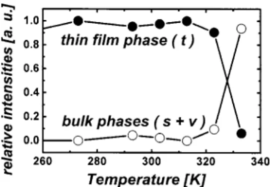
In Fig. 2, the x-ray pattern of the/ 2 scans for penta-cene films prepared at 77, 293, 323, and 333 K is shown. The absence of diffraction peaks for the 77 K film indicates the missing of detectable long-range order. On the other hand, elevated temperatures during the film growth induce order. At 293 K, mainly the thin-film phase t grows on the substrate. Beginning with 323 K, also a small amount of the single-crystal phase s is detected. At a transition temperature of about 330 K, just a few degrees below the temperature where multilayer films could not be made anymore under vacuum conditions, the crystal growth mode changes again considerably. The main polymorphs at this deposition tem-perature are the two single-crystal structures. Figure 3 illus-trates this dramatic change in the structural composition of the films. At higher angles of the / 2 scans 共not shown兲, copper peaks were also detected. With the Scherrer method57 the crystallite size of the copper substrate could be deter-mined to be approximately 10 nm for all the samples.
This transition and the coexistence of the single-crystal phase and the thin-film phase have already been reported for growth on passivated 共oxidized兲 surfaces of SiO2
共Refs. 36–42兲 and for Al2O3共Ref. 43兲 as well as for Corning glass.44 To the knowledge of the authors a coexistence of three of the polymorphs of pentacene has not been reported until now. To distinguish between the various phases, high-resolution measurements are required, especially since the vapor-deposition and single-crystal phases have a very simi-lar d共001兲 spacing. In Fig. 2, the two bulk phases are clearly distinguished in the x-ray pattern for the 333-K film. This pattern also indicates that the crystallites for these three pen-tacene polymorphs have predominantly a 共001兲 orientation. That is, the molecules are standing on the substrate surface with the long molecular axes perpendicular to the surface 共end-on alignment兲.
In the Bragg-Brentano geometry, reflections of net planes parallel to the surface of the substrate are detected. The line-profile analysis of these high-resolution patterns re-veals information on the crystallite size and the strain in the direction perpendicular to the substrate surface. The accuracy of the line-profile analysis depends crucially on the separa-tion of the instrumental broadening from the intrinsic line-width generated by the sample itself. For an analytical ex-pression of the broadening of the instrument, the model of Caglioti et al.58 was adopted using the LaB6 standard. In order to separate the two remaining intrinsic contributions, due to strain and the size of the crystallites, from each other, a Williamson-Hall analysis59is applied:
FIG. 1. Chemical structure of pentacene.
FIG. 2. / 2scans of thin pentacene films deposited at substrate tempera-tures of 77, 293, 323, and 333 K onto polycrystalline Cu substrates, indicat-ing the evolution of three different polymorphs with the substrate tempera-ture during deposition of pentacene. The abbreviation of the peaks t, s, and
v denote the thin-film, the single-crystal, and the vapor-deposition phases,
respectively.
FIG. 3. Evolution of the relative intensities of the thin-film phase共䊊兲 with respect to the two bulk phases共쎲兲 as a function of the substrate temperature during the deposition of the organic material.
b共s兲 = 1/具l典V+
冑
2共⑀2兲 · s. 共1兲Here, s is the length of the scattering vector, b共s兲 is the integral width of the peak, and具l典V is the volume-weighted
column length which is in this case the volume-weighted crystal size perpendicular to the surface. 具⑀2典 is the mean-square 共local兲 strain, whereas the whole root expression is the root-mean-square strain共rms strain兲.
The scattered intensity for the共001兲 net planes and its higher-order共002兲 and 共003兲 reflections from the/ 2scans depicted in Fig. 2 were high enough to allow a peak profile analysis. Pseudo-Voight-shaped profile functions were used to fit the individual peaks.60,61 The Williamson-Hall plots are depicted in Fig. 4. For each sample the three points are on line which reveal the desired parameters: 1 /具l典V
=共0.0077±0.0009兲 cm−1 and rms strain=共0.0059±0.0006兲 for the 293 K sample, 1 /具l典V=共0.0066±0.0009兲 cm−1 and
rms strain=共0.0064±0.0007兲 for the 323 K sample, as well as 1 /具l典V=共0.0115±0.0005兲 cm−1 and rms strain
=共0.0047±0.0003兲 for the 333 K sample. From this fit pa-rameters, the volume-weighted size of the crystallites per-pendicular to the substrate surface amounts to共129±15兲 nm for the 293 K sample, 共150±20兲 nm for the 323 K sample, and共87±4兲 nm for the 333 K sample.
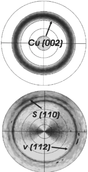
In addition to the symmetric/ 2 measurements, x-ray pattern in pole-figure geometry were recorded. In this geom-etry, net planes that are inclined with respect to the substrate can also be observed. The distribution of a single net plane specified by the 2 value of the sample is recorded and re-sults in the determination of the spherical distribution of that net plane. As the index of the net plane parallel to the sub-strate surface is already known from the / 2 scans, the appropriate distribution of the azimuthal crystallite orienta-tion is uniquely determined46,48and represented in the pole figures. Figure 5 shows two of these patterns: the upper one is recorded for the 共002兲 plane of copper, while the lower pattern shows the distribution of planes with the net plane distance of 4.5 Å for the pentacene film deposited at 333 K. For this distance, the net planes from the single-crystal struc-ture s, 共110兲, and from the vapor-deposition structure v, 共112兲, generate intensities. Both planes are easily distin-guished as they appear at different angles with respect to the 共001兲 plane visible by the different ring radii in the pole
figure. A rather homogeneous distribution of pole densities along the rings implies that while the specific net plane is essentially parallel to the substrate surface, the azimuthal angle of this plane is equally distributed. That is, the azi-muthal orientation of the crystallites is random. This type of distribution of pole densities along the rings is called “fiber texture”共see Fig. 5兲.
The radial pole density along a line through the center of the pole figure is a rocking curve. The peak width of the rocking curves 共which means in this case the width of the recorded rings兲 is a measure of the spread and alignment of the crystallites with respect to the substrate. For the penta-cene film made at 333 K, the width of the Cu pole densities 共see Fig. 5, upper pole figure兲 is much larger than that of the individual pentacene rings. Crystallites of the copper sub-strate are therefore less aligned to each other than those of the organic layer.
The main result of this study is that major parts of the pentacene films grown at ambient substrate temperatures have a共001兲 orientation 共end-on兲 independent of the specific FIG. 4. Williamson-Hall plot of pentacene films deposited at 293, 323, and
333 K. The lines connecting the peak series are linear least-squares fits. The inverse of the ordinate interception equals the volume-weighted size of the crystallites in the film. The slope represents the root-mean-square strain.
FIG. 5. Pole figure of the copper substrate共above兲 and the pentacene layer deposited at 333 K共below兲. Both show a fiber texture but the angular spread of the alignment of copper is much higher as it is for the pentacene layer and its polymorphs, as indicated by the width of the rings.
distribution of crystal phases. This particular orientation of the crystallites is remarkably different as on many metallic surfaces pentacene molecules are lying共flat-on兲,62,63leading to a clearly different alignment of the net planes.64–68A flat-on or edge-flat-on arrangement is observed for a number of or-ganic molecules on single-crystal surfaces. For example, the rodlike molecule quaterphenyl 共with an isomorph crystal structure兲 prefers to lie when deposited on the Au共110兲 substrates.69,70 Other examples are large discotic polyaro-matic molecules, such as copper phthalocyanine and hexa-peri-hexabenzocoronenes, which in films of a thickness simi-lar to that in our films are oriented flat-on on the Au共110兲 and MoS2共0001兲 single-crystal surfaces, respectively.56,71 Note that on the technically relevant polycrystalline substrates, the orientation of both copper phthalocyanine71 and pentacene molecules is radically different from that in films grown on single crystals.
In the present pentacene/polycrystalline Cu system, the domains in the substrate are typically smaller than 10 nm, not much larger than the length of the molecules of about 1.5 nm. Since the molecular orientation is different to that on single-crystal substrates and since the lateral size of penta-cene crystallites is far larger than that of the domains in the underlying substrate, it is obvious that the formation of pen-tacene crystallites is not driven by the interaction with the substrate. It appears that the substrate domains are too small
to form a template suitable to initiate epitaxial growth. These considerations might explain why the pentacene crystallites grow end-on.
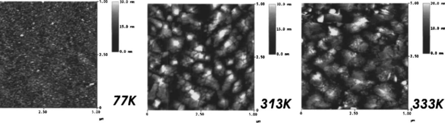
TM-SFM images of layers grown at different tempera-tures are presented in Fig. 6. The film grown at 77 K shows very small grains. Since the x-ray pattern is featureless, a long-range order in these grains is missing. At elevated tem-peratures, the grains become larger and a terracelike mor-phology develops which is consistent with an end-on ar-rangement of the molecules. The transition from the thin-film phase to the bulk phases does not change the morphology of the films.
Additionally to the terracelike morphology needles have been observed in films prepared at various substrate tempera-tures. Figure 7 shows such a structure for a 303-K film. Needlelike structures sometimes result from molecules lying at the substrate.51,52 For such an orientation, Bragg reflec-tions other than those of the共001兲 series have to be present in the x-ray pattern. And indeed, a peak at around 24.1° in the/ 2scan of the film deposited at 323 K共Fig. 8兲 cannot be explained in terms of the 共001兲 orientations of the net planes parallel to the substrate surface. This position matches the 共022兲 peak of the polymorph v.44 The same peak is present for films made on Corning glass,44 but it is not
FIG. 7. TM-SFM image of a pentacene film deposited at a substrate tem-perature of 303 K showing a needlelike structure. The overview shows a 5⫻5m2region of the sample. The three-dimensional image is a close-up region of 2⫻2m2displaying details of the needle morphology.
FIG. 6. The morphology of pentacene films deposited on polycrystalline copper substrates at different substrate temperatures. All TM-SFM images show 5⫻5m2sections of the surface. The gray scale ranges from 0 to 30 nm for the films prepared at 77 and 313 K. For the third image the scale ranges from 0 to 20 nm.
FIG. 8. / 2scans of pentacene thin films deposited at substrate tempera-tures of 323 and 333 K. The scan of the film deposited at 323 K shows clearly an additional orientation to the共001兲 orientation.
indexed. The 共022兲 plane is also a cleavage plane 共Fig. 9兲 and indicates that the growth of the needles occurs with this plane parallel to the substrate.
From the TM-SFM images in Fig. 6, the lateral dimen-sions of the grains can be estimated to be about 1m in diameter. However, it should be assumed that individual grains consist of more than one crystallite. As the substrate is not seen in the images, the height of the crystallites is not accessible by TM-SFM. This parameter can be determined by a line-profile analysis of the x-ray measurements shown in Fig. 4 followed by a size/strain analysis. The average height increases from about 129 nm at 293 K to about 150 nm at 323 K. In the transition region at about 333 K, where a mixture of all three polymorphs is present, the crys-tallite size is with about 87 nm considerably lower. The evaluation of the rms strain within the film rounds up the picture: 0.0059 at 293 K, 0.0064 at 323 K, and 0.0047 at 333 K. That is, strain is mainly constant near the transition point at 330 K and is released at higher temperature.
IV. CONCLUSION
The growth of thin pentacene films on technically rel-evant polycrystalline copper substrates has been studied as a function of the substrate temperature during the deposition of the organic film. While at low temperatures共77 K兲 a long-range order is missing, at ambient temperatures molecules are mobile enough to form a multitude of crystalline phases. In particular, three different polymorphs are observed where the composition of the films changes at a phase-transition temperature of about 330 K from the thin-film polymorph to the two single-crystal bulk structures. However, independent of the temperature, the large majority of crystallites align with the 共001兲 net planes parallel to the substrate. Only a minor contributions are needlelike structures where the mol-ecules have a flat-on arrangement with respect to the sub-strate surface.
The observed dominant end-on molecular alignment and therefore the orientation of crystallites are remarkably differ-ent from that in pdiffer-entacene films grown on single-crystal cop-per surfaces. Evidence is found that the texture of the organic films does not follow the texture of the underlying polycrys-talline copper substrate. This indicates that when the grains in the substrate are too small, the interaction between the molecules and the surface becomes too weak to allow epi-taxial growth.
eral crystalline phases cannot be avoided when using poly-crystalline copper substrates but is controlled by the choice of the deposition parameters and the substrate quality. Con-sequences for the transport of charge carriers and for the functioning of organic electronic devices based on pentacene may be severe and remain to be investigated in detail.
ACKNOWLEDGMENTS
This research project is supported by the Austrian Sci-ence Foundation共Project No. P15626-PHY兲 and the foreign affairs division of the Graz University of Technology. One of the authors共M.O.兲 also acknowledges support from the Aus-trian Research Society 共ÖFG兲. The work performed in Linköping is supported by the Swedish Science Council 共VR; Project No. 12252020兲, partially by the EU-Growth project MAC-MES共Project no. GRD2-2000-30242兲, and by the Center for Advanced Molecular Materials 共CAMM兲 funded by SSF.
1A. Pochettino, Acad. Lincei Rend. 15, 355共1906兲.
2N. Karl, Organic Semiconductors, Landolt-Börnstein, New Series, Group III, Vol. 17共Springer-Verlag, Berlin, 1985兲.
3Y. Y. Lin, D. J. Gundlach, S. F. Nelson, and T. N. Jackson, IEEE Trans. Electron Devices 44, 1325共1997兲.
4Z.-T. Zhu, J. T. Mason, R. Dieckmann, and G. G. Malliaras, Appl. Phys. Lett. 81, 4643共2002兲.
5M. Halik, H. Klauk, U. Zschieschang, T. Kriem, G. Schmid, W. Radlik, and K. Wussow, Appl. Phys. Lett. 81, 289共2002兲.
6M. Kitamura, T. Imada, and Y. Arakawa, Appl. Phys. Lett. 83, 3410 共2003兲.
7J. Zaumseil, T. Someya, Z. Bao, Y.-L. Loo, R. Cirelli, and J. A. Rogers, Appl. Phys. Lett. 82, 793共2003兲.
8Y. S. Lee, J. H. Park, and J. S. Choi, Opt. Mater.共Amsterdam, Neth.兲 21, 433共2002兲.
9S. Kuniyoshi, S. Naruge, M. Iizuka, M. Nakamura, K. Kudo, and K. Tanaka, Synth. Met. 137, 895共2003兲.
10J. Lee, D. K. Hwang, C. H. Park, S. S. Kim, and S. Im, Thin Solid Films
451, 12共2004兲.
11G. Jarosz, R. Signerski, and J. Godlewski, Synth. Met. 109, 161共2000兲. 12G. Jarosz, R. Signerski, and J. Godlewski, Thin Solid Films 396, 196
共2001兲.
13J. Godlewski, G. Jarosz, and R. Signerski, Appl. Surf. Sci. 175, 344 共2001兲.
14R. Signerski, G. Jarosz, and J. Godlewski, Synth. Met. 94, 135共1998兲. 15Y. Vertsimakha and A. Verbitsky, Synth. Met. 109, 291共2000兲. 16J. Lee, S. S. Kim, K. Kim, J. H. Kim, and S. Im, Appl. Phys. Lett. 84,
1701共2004兲.
17S. S. Kim, Y. S. Choi, K. Kim, J. H. Kim, and S. Im, Appl. Phys. Lett.
82, 639共2002兲.
18S. P. Park, S. S. Kim, J. H. Kim, C. N. Whang, and S. Im, Appl. Phys. Lett. 80, 2872共2002兲.
19G. K. R. Senadeera, P. V. V. Jayaweera, V. P. S. Perera, and K. Tenna-kone, Sol. Energy Mater. Sol. Cells 73, 103共2002兲.
20D. J. Gundlach共private communication兲.
21R. G. D. Valle, E. Venuti, A. Brillante, A. Girlando, ChemPhysChem 5, 266共2004兲.
22D. J. Gundlach, T. N. Jackson, D. G. Schlom, and S. F. Nelson, Appl. Phys. Lett. 74, 3302共1999兲.
23R. B. Campbell, J. M. Robertson, and J. Trotter, Acta Crystallogr. 14, 705共1961兲.
24R. B. Campbell, J. M. Robertson, and J. Trotter, Acta Crystallogr. 15, 289共1962兲.
25D. Homes, S. Kumaraswamy, A. J. Matzger, and K. P. Vollhardt, Chem.-Eur. J. 5, 3399共1999兲.
FIG. 9. Schematic drawing of the pentacene net plane共022兲 of the vapor-deposition phase v.
26C. C. Mattheus, A. B. Dros, J. Baas, A. Meetsma, J. L. de Boer, and T. T. M. Palstra, Acta Crystallogr., Sect. C: Cryst. Struct. Commun. 57, 939 共2001兲.
27C. C. Mattheus, A. B. Dros, J. Baas, G. T. Oostergetel, A. Meetsma, J. L. de Boer, and T. T. M. Palstra, Synth. Met. 138, 475共2002兲.
28C. C. Mattheus, G. A. de Wijs, R. A. de Groot, and T. T. M. Palstra, J. Am. Chem. Soc. 125, 6323共2003兲.
29G. A. de Wijs, C. C. Mattheus, R. A. de Groot, and T. T. M. Palstra, Synth. Met. 139, 109共2003兲.
30T. Minakata, H. Imai, M. Ozaki, and K. Saco, J. Appl. Phys. 72, 5220 共1992兲.
31T. Minakata, H. Imai, and M. Ozaki, J. Appl. Phys. 72, 4174共1992兲. 32J. E. Northrup, M. L. Tiago, and S. G. Louie, Phys. Rev. B 66, 121404
共2002兲.
33F.-J. zu Heringdorf, M. C. Reuter, and R. M. Tromp, Nature共London兲
412, 517共2001兲.
34R. Ruiz, B. Nickel, N. Koch, L. C. Feldman, R. F. Haglund, A. Kahn, and G. Scoles, Phys. Rev. B 67, 125406共2003兲.
35L. Farina, A. Brillante, R. G. D. Valle, E. Venuti, M. Amboage, and K. Syassen, Chem. Phys. Lett. 375, 490共2003兲.
36C. D. Dimitrakopoulos, A. R. Brown, and A. Pomp, J. Appl. Phys. 80, 2501共1996兲.
37D. J. Gundlach, Y. Y. Lin, T. N. Jackson, S. F. Nelson, and D. G. Schlom, IEEE Electron Device Lett. 18, 87共1997兲.
38D. Knipp, R. A. Street, B. Krusor, R. Apte, and J. Ho, J. Non-Cryst. Solids 299, 1042共2002兲.
39D. Knipp, R. A. Street, A. Völkel, and J. Ho, J. Appl. Phys. 93, 347 共2003兲.
40M. Shtein, J. Mapel, J. B. Benzinger, and S. R. Forrest, Appl. Phys. Lett.
81, 268共2002兲.
41T. Jentzsch, H. J. Juepner, K.-W. Brzezinka, and A. Lau, Thin Solid Films 315, 273共1998兲.
42I. P. M. Bouchoms, W. A. Schoonveld, J. Vrijmoeth, and T. M. Klapwijk, Synth. Met. 104, 175共1999兲.
43J. Lee, J. H. Kim, and S. Im, J. Appl. Phys. 95, 3733共2004兲. 44J. Puigdollers, C. Voz, A. Orpella, I. Martin, M. Vetter, and R. Alcubilla,
Thin Solid Films 427, 367共2003兲.
45R. Friedlein, X. Crispin, M. Pickholz, M. Keil, S. Stafström, and W. R. Salaneck, Chem. Phys. Lett. 354, 389共2002兲.
46L. E. Alexander, X-Ray Diffraction Methods in Polymer Science共Robert E. Krieger, Huntington, New York, 1979兲.
47B. Servet, S. Ries, M. Trotel, P. Alont, G. Horowitz, and F. Garnier, Adv. Mater.共Weinheim, Ger.兲 5, 461 共1993兲.
48J. Kečkeš, B. Ortner, J. Jakabovič, and F. Kováč, J. Cryst. Growth 192, 84共1998兲.
49S. R. Forrest, Chem. Rev.共Washington, D.C.兲 97, 1030 共1997兲. 50S. R. Forrest, M. L. Kaplan, and P. H. Schmidt, J. Appl. Phys. 56, 543
共1984兲.
51R. Resel, Thin Solid Films 433, 1共2003兲.
52H. Plank, R. Resel, S. Purger, J. Keckes, A. Tierry, B. Lotz, A. Andreev, N. S. Sariciftci, and H. Sitter, Phys. Rev. B 64, 235423共2001兲. 53L. G. Schultz, J. Appl. Phys. 20, 1030共1949兲.
54W. Kraus and G. Nolzeb, J. Appl. Crystallogr. 29, 301共1996兲. 55I. Salzmann and R. Resel, J. Appl. Crystallogr. 37, 1029共2004兲. 56R. Friedlein, X. Crispin, C. Simpson et al., Phys. Rev. B 68, 195414
共2003兲.
57B. E. Warren, X-Ray Diffraction共Addison-Wesley, Reading, MA, 1969兲. 58G. Caglioti, A. Paoletti, and R. Ricci, Nucl. Instrum. Methods 35, 223
共1958兲.
59G. Williamson and W. Hall, Acta Metall. 1, 22共1953兲.
60R. Snyder, J. Fiala, and H. Binge, IUCr Monographs on Crystallography 10共Oxford University Press, New York, 1999兲.
61R. Young, IUCr Monographs on Crystallography 5共Oxford University Press, New York, 1993兲.
62S. Lukas, S. Söhnchen, G. Witte, and C. Wöll, ChemPhysChem 5, 266 共2004兲.
63S. Lukas, G. Witte, and C. Wöll, Phys. Rev. Lett. 88, 028301共2002兲. 64V. Corradini, C. Menozzi, M. Cavallini, F. Biscarini, M. G. Betti, and C.
Mariani, Surf. Sci. 532, 249共2003兲.
65C. Menozzi, V. Corradini, M. Cavallini, F. Biscarini, M. G. Betti, and C. Mariani, Thin Solid Films 428, 227共2003兲.
66Y. L. Wang, W. Ji, D. X. Shi, S. X. Du, C. Seidel, Y. G. Ma, H.-J. Gao, L. F. Chi, and G. Fuchs, Phys. Rev. B 69, 075408共2004兲.
67J. H. Kang and X.-Y. Zhu, Appl. Phys. Lett. 82, 3248共2003兲. 68P. G. Schroeder, C. B. France, J. B. Park, and B. A. Parkinson, J. Appl.
Phys. 91, 3010共2002兲.
69S. Müllegger, I. Salzmann, R. Resel, and A. Winkler, Appl. Phys. Lett.
83, 4536共2003兲.
70S. Müllegger, O. Stranik, E. Zojer, and A. Winkler, Appl. Surf. Sci. 221, 184共2004兲.
71H. Peisert, T. Schwieger, J. M. Auerhammer, M. Knupfer, M. S. Golden, J. Fink, P. R. Bressler, and M. Mast, J. Appl. Phys. 90, 466共2001兲.