Development of Partially-thinned LAPS
Structures and Their Applications to Chemical
Imaging and Analysis of Multiple Samples
著者
チューン ホアン アン
学位授与機関
Tohoku University
学位授与番号
11301甲第18813号
Development of Partially-thinned LAPS Structures and Their
Applications to Chemical Imaging and Analysis of Multiple Samples
Tohoku University
Department of Biomedical Engineering
Thesis advisor
Tatsuo Yoshinobu
Thesis submitted for the degree of Doctor of Philosophy
by
Hoang Anh Truong
Date of submission
March 2018
Abstract
- 1 -
Abstract
The development of biochemical sensors responds to the demand of biochemical analysis in various fields. Semiconductor-based field-effect biochemical sensors have generated considerable research interest in quantitative analysis of chemical and biological analytes in environmental monitoring, clinical diagnosis and drug screening platforms. They have advantages of compact size, fast response and possibility of low-cost fabrication. The chemical imaging sensor based on the principle of the light-addressable potentiometric sensor (LAPS) has been a key technique for detecting the distribution of target ions in the sample on its sensing surface for some decades, which is expected to be an effective detection tool for chemical and biochemical analytes. In addition, the chemical imaging sensor based on the principle of LAPS is considered as a highly potential multi-analyte, multi-sample sensor due to its possibility of spatially resolved detection of ion concentration on its sensing surface addressed by a focused light beam.
The spatial resolution and the measurement speed are both very important to the performance of the chemical imaging sensor, and much effort has been focused on improving them. It has been demonstrated that a thin sensor plate could achieve a higher resolution because of the restriction of carrier diffusion. It has been also demonstrated that a thin sensor plate could improve the signal-to-noise ratio at higher frequencies, which would be advantageous for high-speed measurements. However, the fragileness of a thin sensor plate is a problem for practical applications, where not only solutions but also various types of samples are to be brought into contact with the sensing surface. In this thesis, new structures of LAPS, which are advantageous in the spatial resolution, the measurement speed as well as the mechanical strength, are demonstrated. Furthermore, its applications and benefits in measuring a plurality of liquid samples on a single sensor plate without the need of additional multi-chamber structures are investigated. This sensor can be applied to environmental and industrial analysis as well as biomedical applications, where a plurality of biological samples must be incubated under the same conditions.
Abstract
- 2 -
Partially-etched structures of the LAPS sensor plate, which strikes a balance between the imaging performance and the mechanical strength of the sensor plate, were fabricated by optimization of an anisotropic etching process based on tetramethylammonium hydroxide (TMAH). Accordingly, based on the improvement of the newly fabricated partially-etched LAPS sensor plate, a multi-well LAPS sensor plate was developed, which functions as an integrated array of pH sensors. A SiO2 film was formed on the partially-etched substrate as a pH sensing surface. Each well can be loaded with a few μL of solution to be individually analyzed. The different pH solutions were used to investigate the variation of the sensor sensitivity. As an application to biological samples, the metabolic activities of Escherichia
coli (E. coli) was investigated by measuring the extracellular acidification of different E. coli
concentrations.
As a result, there are two impact results obtained in this thesis:
1. Development of a partially-etched sensor plate. A LAPS sensor plate with a partially-etched structure was newly fabricated and realized a high signal-to-noise ratio, high-resolution and high-speed measurement while maintaining the overall mechanical strength. Thanks to the partial etching, the spatial resolution was improved from 4 0 to 20 μm. The enhanced photocurrent in the etched region is obtained as a result of reduced loss of carriers due to the shorter travelling distance of photocarriers by diffusion, which leads to an improvement in high-speed chemical imaging due to the broader bandwidth. This structure was further developed into a multi-well LAPS which is not only advantageous for higher photocurrent and higher spatial resolution but also high-throughput measurement in comparison to the conventional flat LAPS sensor plate. It is capable of measuring a plurality of sample solutions on a single sensor plate without the need for additional multi-chamber structures, e.g., due to multiple wells on the sensing surface.
2. Applications to chemical imaging and analysis of multiple samples. The device can be applied, for example, to quantification of metabolic activities and imaging of biological samples incubated in the well, and to multi-analyte sensing of metabolism and screening of cells cultured inside different wells. Measurement of different concentrations of E. coli on a single sensor plate has clarified the different acidification rates by growing cells. Furthermore, to simplify the sample dispensing mechanism, a fluid channel, which was built onto the sensor surface, could dispense solution into different wells.
Acknowledgments
- 3 -
Acknowledgments
I would like to express my sincere gratitude to my advisor Professor Tatsuo Yoshinobu for his support of my PhD for his immense knowledge, motivation and patience. His guidance helped me in all the time of research and writing of this thesis. Professor Yoshinobu has been supportive, has given me the freedom to pursue my research and inspired me to follow my dreams. He has also provided insightful discussion about the research and has helped me with proofreading all the manuscript.
Besides my advisor, I would like to thank Professor Ko-ichiro Miyamoto, for his insightful comments and encouragement in my experiments to widen my research form various perspectives. My sincere thanks also go to Dr. Carl Frederik Werner for his scientific advice, knowledge and many helpful discussion and suggestions. He was my primary resource for getting my questions answered and was instrumental in helping me to write my papers, during my study.
I would like to thank Professor Michael. J. Schöning (Aachen University of Applied Sciences) for his cooperation in the technical support of my experiments and his fruitful discussion.
I will forever be thankful to my former master research advisor, Professor Sone Hayato in Gunma University, who has inspired me to pursue my dream for studying PhD. His enthusiasm and love for teaching is contagious.
I thank all my lab mates in Yoshinobu-Miyamoto Laboratory, Tohoku University for providing support and friendship that I needed in these past three years. I am also glad that I studied with Mengyuan Wang, an enthusiastic and optimistic friend. I value her friendship and support as well.
I also thank Fundamental Technology Center, Tohoku University for supplying equipment and helping me with making experimental tools and sample evaluation.
I would like to thank the committee members, Professor Yoshifumi Saijo and Professor Yuji Matsuura for their discussion, insightful comments and encouragement.
Acknowledgments
- 4 -
I especially thank my best friend, my soul-mate and my husband, Dr. Dai Igarashi. He has been a great supporter both academically and personally, and unconditionally helped me during my good and bad times. I truly thank him for being with me even when I was irritable and depressed and for taking care of me and our house during writing this thesis. I also thank my parents-in-law who all have been supportive and caring us.
Special thanks to my mom, dad and sisters. My hard-working parents have sacrificed their lives and provided us unconditional love. My sisters have been my best friends all my life and I thank them for all their supports. My sisters are also the first place for me to count on when times are rough.
Last but not least, my research could not be possible without financial supports. I gratefully acknowledge the funding and scholarships from:
⚫ The Japan Science Society, Sasakawa Scientific Research Grant for financial support of the research project.
⚫ The NEC C&C Foundation for their financial support of the travel expense for the international conference of Engineering of Functional Interfaces EnFI 2017.
⚫ The Marubun Research Promotion Foundation for the financial support of the travel expense for the international conference of 6th International Symposium on Sensor Science (I3S 2018).
⚫ Japan Tobacco INC for the scholarship during the first two years of PhD study. ⚫ Otsuka Toshimi Scholarship Foundation for the third year of PhD study.
Contents - 5 -
Contents
Abstract ... 1 Acknowledgments ... 3 Contents ... 5 List of tables ... 8 List of figures ... 9 -1.Introduction ... 151.1. Overview of the study ... 15
1.2. Semiconductor-based field-effect sensors ... 17
1.3. Light-addressable potentiometric sensor (LAPS) ... 20
1.3.1.Detection principles and application ... 20
1.3.2.Spatial resolution improvement based on the sensor structure ... 22
1.4. Anisotropic partial etching process ... 24
1.5. Summary and outline of the work ... 26
2.Partially-etched structure on the backside of LAPS sensor plate ... 29
2.1. Introduction ... 29
2.2. Mechanical strength of different structures of sensor plates ... 32
2.3. Fabrication process of partially-etched sensor plate ... 33
2.4. Measurement method ... 37
Contents
- 6 -
2.5.1.Characteristics of the partially-etched sensor plate ... 39
2.5.2.pH sensitivity ... 42
2.5.3.Improvement of photocurrent signal ... 44
2.5.4.Improvement of frequency bandwidth ... 47
2.5.5.Improvement of lateral spatial resolution ... 48
2.6. Summary ... 50
3.Multi-well sensor based on partially-etched structure on the frontside of LAPS sensor plate ... 53
3.1. Introduction ... 53
3.2. Fabrication process and measurement system ... 56
3.3. Experimental results ... 59
3.3.1.Characterization of multi-well LAPS sensor ... 59
3.3.2.The in-plane uniformity ... 62
3.3.3.Measurement of pH buffer solutions on a single sensor chip ... 64
3.3.4.Lateral spatial resolution in a well ... 66
3.3.5.Frequency bandwidth ... 68
3.3.6.Imaging of different pH buffer solutions ... 69
3.4. Summary ... 71
4.Measurement of Escherichia coli metabolism with multi-well LAPS ... 73
4.1. Introduction ... 73
4.2. Incubation of Escherichia coli (E. coli) ... 75
4.3. Visualization of E. coli colony ... 78
Contents
- 7 -
4.4.1.Measurement of different cell concentrations of E. coli ... 80
4.4.2.Set-up for long-term measurement on a chip ... 83
4.5. Summary ... 90
5.Microfluidic channel for dispensing samples into multiple wells ... 91
5.1. Review of LAPS combined with microfluidics ... 91
5.2. Microfluidic channel for dispensing solutions ... 93
5.3. Characterization... 94
5.4. Summary ... 97
6.Conclusions ... 99
References ... 103
Appendix a: publications ... 109
List of tables
- 8 -
List of tables
Table 1.1 Dependence of the etching rate and the surface roughness on etching parameters.
... 25
Table 2.1 Temperature program for the thermal oxidation process. ... 34
Table 2.2 Parameters for I-V measurement. ... 43
Table 3.1 pH sensitivity and deviation of the flat-band voltage observed in 9 wells. ... 63
Table 4.1 Ingredients for the LB medium suspended in 1 L of deionized water. ... 76
Table 4.2 The samples measured in wells 1 – 9 and number of E. coli cells included in 0.35 µL of samples incubated in wells 5 – 9. ... 85
1.1 Overview of the study
- 9 -
List of figures
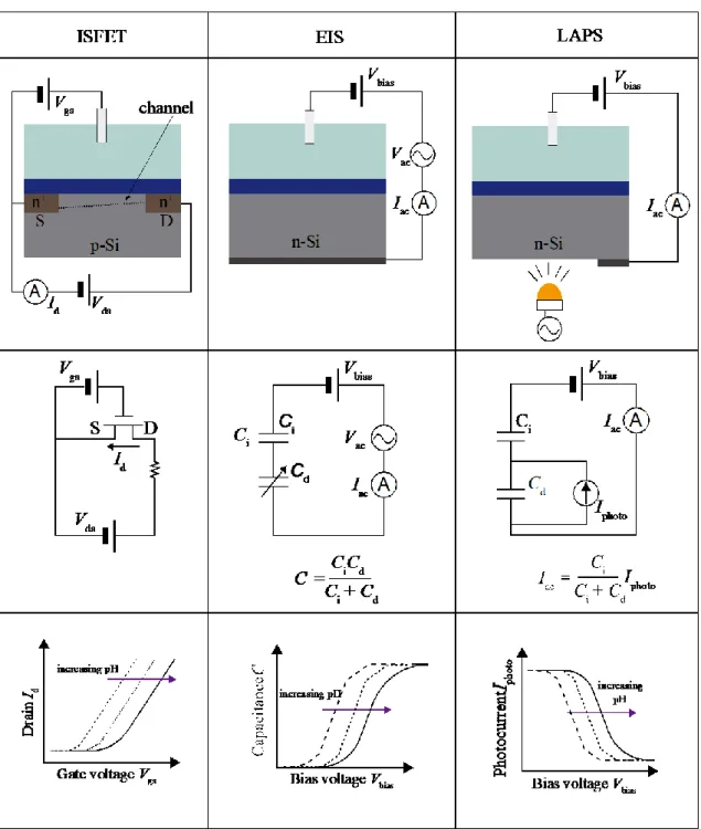
Figure 1.1 Schematic of a chemical sensor. ... 16
Figure 1.2 Structures, equivalent circuits and signals of ISFET, capacitive EIS sensor and LAPS. ... 19
Figure 1.3 Configuration of a LAPS... 22
Figure 1.4 (a) Dependence of the spatial resolution of a LAPS on its thickness. (b) Relation of sensor thickness and spatial resolution. ... 23
Figure 1.5 Facets observed after etching of Si (100) by TMAH. ... 25
Figure 2.1 Schematic of a LAPS sensor plate with partially-etched structures on the back side. ... 31
Figure 2.2 Simulation of mechanical deflections in 3 types of sensor plates; a t hick sensor plate, a partially-etched sensor plate and a thin sensor plate. ... 32
Figure 2.3 Fabrication process of a partially-etched sensor plate. ... 33
Figure 2.4 Back surface of the sensor plate before and after thermal oxidation at 900°C for 5 h and 10 h. ... 34
Figure 2.5 (a) Apparatus used for anisotropic etching of Si by 25% TMAH at 90 ± 2°C and (b) the view of the etching set-up. To be safe, heating system including hot plate, water tub and flask were put inside a fume hood. ... 36
1.1 Overview of the study
- 10 -
Figure 2.7 Optical images of the back surface of a LAPS sensor plate (a) after forming a circular opening in the resist film by photolithography, (b) after removing SiO2 inside the circular opening by 5% HF followed by removal of the resist film, and (c) after anisotropic etching of Si by TMAH. ... 37
Figure 2.8 Measurement system for modulation frequencies lower than 10 kHz. ... 38
Figure 2.9 Measurement system for modulation frequencies higher than 10 kHz (used in the measurement of frequency characteristics). ... 38
Figure 2.10 Test pattern with different widths of resist stripes formed on the sensing surface of a partially-etched LAPS sensor plate. ... 39
Figure 2.11 Sensor holder for LAPS measurement. ... 40
Figure 2.12(a) Optical image of the partially-etched structures on the back surface of the LAPS sensor plate. (b) Cross-sectional SEM image at the border of the etched region and the frame region. ... 41
Figure 2.13 SEM images of (a) the surface at the bottom of the etched structure, (b) the back surface of the frame region, (c) cross section at the border of the etched region and the frame region and (d) pyramidal structures found at the bottom of the etched region. ... 42
Figure 2.14 (a) Photocurrent - bias voltage curves and (b) normalized photocurrent - bias voltage curves for different pH buffer solutions measured in the frame region and the etched region, respectively... 43
Figure 2.15 pH-dependence of the bias voltage at the inflection point of the I-V curve measured in the frame region and the etched region. ... 44
Figure 2.16 (a) Optical image of an etched region with ϕ 6 mm. (b) Distribution of the photocurrent around the etched region obtained with pH7 buffer solution. ... 45
Figure 2.17 (a) Photocurrent vs scanning position starting from the center of the etched region of a partially-etched sensor plate which have one etched region with ϕ 6 mm. (b) I-V curves measured at different locations shown in (a). ... 45
Figure 2.18 (a) I-V curves acquired in the frame region and the etched region, respectively. (b) Photocurrent image acquired at a bias voltage of -0.5 V for pH 7 buffer solution in contact with the sensing surface of a partially-etched LAPS sensor plate. ... 46
1.1 Overview of the study
- 11 -
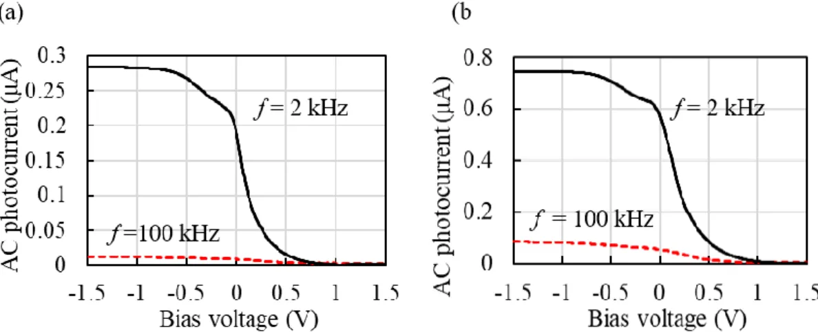
Figure 2.19 I-V curves for pH 7 buffer solution acquired at 2 kHz and 100 kHz in (a) the frame region and (b) the etched region, respectively. ... 47
Figure 2.20 Frequency characteristics of the photocurrent signal obtained in the frame region and the etched region, respectively. ... 48
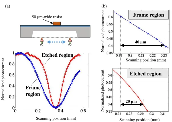
Figure 2.21 (a) Line scanning perpendicular to a 50-um-wide resist pattern. (b) Line profiles of the normalized photocurrent across the resist pattern in the etched region and the frame region, respectively. (c) Comparison of the lateral distance, in which the normalized photocurrent decays from 60% to 40% of the maximum value, in the frame region and the etched region, respectively. ... 49
Figure 2.22 Photocurrent images of a test pattern in the frame region and the etched region, respectively. The widths of the resist patterns were 20, 40 and 100 µm. ... 50
Figure 3.1 Comparison of the partially-etched structures on (a) the back side and (b) the front side of the LAPS sensor plate. ... 55
Figure 3.2 Multi-well sensor plate with partially-etched structures on the front side. (a) Liquid samples accommodated in an array of wells can be independently analyzed by light addressing. (b) Schematic of the cross section of a well and the frame region. The thinner active region at the bottom of a well results in less diffusion of minority carriers. ... 55
Figure 3.3 Fabrication process of a multi-well LAPS sensor plate. ... 57
Figure 3.4 Apparatus for dry thermal oxidation. ... 57
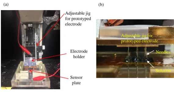
Figure 3.5 (a) Setup for adjusting the height of an array of 9 Pt wire electrodes to individually contact the solutions accommodated in 9 wells on the multi-well LAPS sensor plate. (b) Close-up of 9 Pt wire electrodes contacting the solutions. For better visibility of the contact, an amount of solution in excess of the capacity of the well was pipetted into each well. ... 58
Figure 3.6 Potential difference between a Pt wire electrode and a Ag/AgCl reference electrode measured over a time period of 1 h in 3M NaCl solution and pH buffer solutions of pH 1, 3, 5, 7 and 9. ... 59
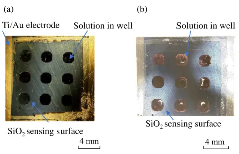
Figure 3.7 (a) Optical image of the front side of a multi-well LAPS sensor plate. (b) Observation of droplets accommodated in 9 wells on the front side of a LAPS sensor plate. ... 60
1.1 Overview of the study
- 12 -
Figure 3.8 (a) Cross-sectional SEM image of the front surface at the border between the etched region and the frame region. The glancing angle was 30. Etch pits are observed on the surface of the frame region, while the well surface is smooth. (b) SEM images of the sensing surface at the bottom of a well on the front side. ... 61
Figure 3.9 Normalized photocurrent image for a pH 7 buffer solution acquired with a 9 -well LAPS sensor plate. ... 61
Figure 3.10 Dependence of Vinfl on pH measured in all 9 wells. ... 63
Figure 3.11 Normalized I-V curves for (a) pH 7 buffer solution in all 9 wells and (b) a series of pH buffer solutions from pH 1 to pH 9 in the corresponding number of well 1 to 9, respectively. ... 64
Figure 3.12 The values of Vinfl for pH 7 buffer solution in all 9 wells and a series of pH buffer solutions from pH 1 to pH 9 in the corresponding number of well 1 to 9, respectively. ... 65
Figure 3.13 The relative change of Vinfl with respect to its value for pH 7, measured for pH buffer solutions of pH 1 to pH 9 in the corresponding number of well 1 to 9. ... 65
Figure 3.14 (a) An optical photograph of the test pattern on the sensing surface. (b) A photocurrent image of the test pattern. (c) A line profile of the photocurrent. The shaded regions show the widths of test patterns. ... 67
Figure 3.15 The frequency characteristic of 3 types of samples: conventional LAPS sensor with sensor thickness of 200 μm, sensor plate with a partially-etched structured on the back surface and multi-well sensor plate. ... 69
Figure 3.16 Photocurrent images of (a) pH 7 buffer solutions in 4 wells and (b) different pH buffer solutions of pH 3, 5, 7 and 9 at a fixed bias voltage of -2.4 V. ... 70
Figure 3.17 (a) Photocurrent change and (b) relative photocurrent change between Figure 3.16(a) and (b). ... 71
Figure 4.1 (a) Metabolic activities of E. coli and (b) their threats to human health. ... 74
Figure 4.2 Optical image of E. coli colonies after 8 hours of incubation. ... 76
Figure 4.3 Two types of tests based on LAPS for analysis of E. coli. (a) Chemical imaging of
1.1 Overview of the study
- 13 -
coli based on the measurement of acidification rate by E. coli cells cultured in liquid culture
medium. ... 77
Figure 4.4 (a) pH measurement of samples by a pH meter in the course of incubation after filling the wells with different initial concentrations of E. coli. (b) Temporal change of pH measured in the course of incubation for 12 hours. ... 77
Figure 4.5 (a) Optical image of E. coli colonies cultured for 8 hours on agarose plate. (b) Photocurrent image of E. coli colonies showing acidification due to metabolism. ... 79
Figure 4.6 (a) Photocurrent - bias voltage curves and (b) normalized photocurrent - bias voltage curves acquired at a location of a colony and at a location without a colony. ... 79
Figure 4.7 Temporal change of Vinfl for samples with different initial concentrations of E. coli measured with the multi-well LAPS sensor plate in the course of 8 hours of incubation. .... 82
Figure 4.8 Relative change of pH for samples with different initial concentrations of E. coli measured with the multi-well LAPS sensor plate ... 82
Figure 4.9 Incubation time needed for a pH change of -0.8 as a function of the initial concentration of E. coli... 83
Figure 4.10 (a) Schematic of a measurement setup and (b) the 3D model image to reduce evaporation of the liquid sample in the course of long-term incubation of E. coli. ... 84
Figure 4.11 (a) Measurement setup and (b) a photo of the sensor surface cover for long-term incubation of E. coli. ... 84
Figure 4.12 Incubation of E. coli cells on a multi-well LAPS sensor plate. Three wells contain pH buffers, one well contains culture medium without E. coli, and five wells contain different concentrations of E. coli in culture medium. ... 85
Figure 4.13 Normalized photocurrent - bias voltage curves measured in nine wells in the course of incubation for 8 h. ... 87
Figure 4.14 Temporal change of Vinfl measured in nine wells in the course of incubation. .. 87
Figure 4.15 Temporal change of Vinfl in nine wells with respect to the initial value of Vinfl for pH 4. ... 88
1.1 Overview of the study
- 14 -
Figure 4.16 Temporal change of pH observed in nine wells in the course of incubation for 8 h. ... 89
Figure 4.17 Incubation time needed for a pH change of -0.8 as a function of the initial concentration of E. coli... 89
Figure 5.1 Microfluidic channel combined with a multi-well LAPS sensor plate. ... 93
Figure 5.2 Construction of microfluidic channel on a multi-well LAPS sensor plate. ... 94
Figure 5.3 Automatic filling of wells by a microfluidic channel. (a) Water (colored for visibility) is injected into the microfluidic channel. (b) Wells are filled with the water. (c) Water remaining in the channel is replaced by silicone oil. ... 95
Figure 5.4 Design of the microfluidic channel for automatic filling of wells. ... 95
Figure 5.5 (a) Optical image of the microfluidic channel after filling the wells with pH 7 buffer solution. (b) Photocurrent image of wells filled with pH 7 buffer solution. (c) Photocurrent - bias voltage curve for pH7 buffer solution obtained at the center of well. .... 96
1.1 Overview of the study
15
Chapter 1
1. Introduction
1.1. Overview of the study
A chemical sensor is defined as a device that is capable of providing analytical information such as concentration and quantity about a particular target of chemical substances.[1] Possible applications in various areas are environmental monitoring, clinical diagnosis and drug screening. An ideal chemical sensor is portable, inexpensive, short-response, high-accuracy, high-sensitivity and capable of instantaneous detection.[1] In this respect, the majority of the research activities have been focused to develop the hardware, modify the sensor surfaces and miniaturize the chip size. Meanwhile, semiconductor has become a key factor as a material of chemical sensors. Semiconductor-based sensors can be fabricated using mature techniques from the novel nanotechnology platforms. So far, silicon-based sensors are still the most powerful component of the semiconductor segment with the attractive features such as controllable electronic response, high sensitivity, reproducibility, mass production ability and affordable cost. The use of other materials such as GaN and AlN are also very potential candidates for high-power and high-frequency applications.[2]
A chemical sensor is formed by two basis parts: a receptor element, which responds to particular analyte molecules, and a physicochemical transducer, which convert s the chemical information into analytical information as shown in Figure 1.1. Electrochemical sensors for aqueous samples are based on electrochemical transduction methods. The signal responses are determined by the surface configuration that links with ion distribution and electron-transfer reactions. Electrochemical sensors include two types: amperometric and
1.1 Overview of the study
16
potentiometric. Amperometric sensors are used in detection of ions based on the electric current due to the reduction and oxidation reaction of an electroactive species when a potential is applied. On the other hand, in potentiometric transduction, ion charges can be determined based on the ion-transfer processes occurring at the interface of ion-sensitive membrane and the test solution. Due to the interaction with the analyte, the ion distribution on the membrane results in the electric charge distribution and potential difference.
Light-addressable potentiometric sensor, the central technique in this thesis, is one type of semiconductor-based sensor, which was first invented by D. Hafeman et al. in 1988.[3] LAPS is able to visualize the distribution of target ions in a sample on its sensing surface in a spatially resolved manner.[4–7] LAPS chips have a simple structure that requires only insulator layer and an ohmic contact on the front side and back side of the semiconductor.[3] This is a great advantage for multi-well sensors for chemical imaging and analysis of different samples by separating plurality of sensing areas.[5,8,9] However, one drawback of the LAPS-based chemical imaging sensor is the limitation of read-out speed and spatial resolution determined by single light beam and a scanning mechanism.[5,10] This thesis focuses on the study of the performance improvements of LAPS for chemical imaging and applications for multi-well sensor array. One of the key techniques for the sensor performance improvement is the partial thinning of the sensor plate, which reduces carrier diffusion.
To promote the understanding of field-effect sensors, this chapter includes an overview of the main properties of semiconductor-based field-effect sensors in Section 1.2, especially LAPS in Section 1.3. Later, an anisotropic etching process for the partially-etched structure, which is advantageous in performance improvement, is discussed in Section 1.4.
Figure 1.1 Schematic of a chemical sensor.
Sample
Receptor
Transducer
Signal
→ Compact size
→ Cheap
→ Fast response
→ High sensitivity
...
1.2 Semiconductor-based field-effect sensors
17 1.2. Semiconductor-based field-effect sensors
Field-effect chemical sensors attract much attention in chemical and biological analysis, environmental monitoring due to their outstanding features such as the high-sensitivity detection, fast response, compact size and low-cost manufacturing.[1] Ion-sensitive field-effect transistor biosensor was first proposed by P. Bergveld in 1970, which has opened great developments of chemical and biosensors based on the detection of potential difference according to the activities of the target ion.[11,12]
There are 3 types of field-effect sensors: ion-sensitive field-effect transistors (ISFETs), electrolyte-insulator-semiconductor (EIS) sensors, light-addressable potentiometric sensors (LAPS).[3,11–14] The ISFETs, EIS sensor and LAPS are known as the basic structures of potentiometric sensors which are sensitive to the electrical charges at their interfaces or sensing surface. Figure 1.2 summarizes the sensor structures, equivalent circuits and sensing mechanisms of ISFETs, EIS and LAPS sensor. We can see they share the same field-effect structure that is made of three components: an electrolyte, an insulator and a semiconductor, in which the insulator serves as the sensing surface. This structure is similar to a conventional metal-insulator-semiconductor structure but the electrolyte containing target ions to be measured has replaced the metallic gate. The electric field generated by the bias voltage between the metal and semiconductor, will control the charge distributions responding to the ion concentrations.[1,15]
The structures of ISFETs, EIS and LAPS sensor with their different ways of signal readout are shown in Figure 1.2. Their simplified circuit models and their different output signal readouts are described as follows:
1. For the ISFET, the drain current-gate voltage curves shift with the surface ion concentration. In this case, the surface potential changes the thickness and conductance of the inversion channel at the insulator-semiconductor interface by the effect of electric field.
2. For the EIS sensor, the capacitance-voltage curves shift with different input analyte concentrations. The surface charges modulate the capacitance of EIS sensor.
3. For the LAPS, the photocurrent-voltage curves shift with the ion concentration of the solution. The surface potential changes the thickness and the capacitance of the depletion layer at the insulator-semiconductor interface.
1.2 Semiconductor-based field-effect sensors
18
Based on these different sensing methods, ISFETs, EIS and LAPS sensor can detect the analyte concentration or the compositions serving in many applications. Sensor multiplexing can be developed to serve as multi-sensor arrays based on the LAPS structure.[14,16,17] The localized surface potential can be detected in a spatially resolved manner with LAPS. One of the attractive points of the field-effect sensors is the possibility of manufacturing by using the conventional microfabrication technologies such as: thermal oxidation, deposition, photolithography and etching. It also brings the advantages of small-size sensors and low-cost fabrication. As a result, the three kinds of sensors have been applied in various fields as biotechnology, drug screening and environmental monitoring such as following types of (bio-)chemical sensors:
⚫ The first application of ISFET as a pH sensor was developed by Bergveld. The insulator of silicon dioxide contacts directly with the solution. The silanol sites at the silicon dioxide can undergo various reactions with acid or alkaline.[11,12]
⚫ Various molecules can be detected based on the immobilization of different enzymes. For example, FETs, EIS sensor and LAPS showed the same sensitive characteristics based on of enzyme penicillinase.[11,12]
⚫ An integration of field-effect sensor and micro-fluidic channel allows detection of chemical reactions in a small volume of solution in a real time.[18][19]
1.2 Semiconductor-based field-effect sensors
19
Figure 1.2 Structures, equivalent circuits and signals of ISFET, capacitive EIS sensor and LAPS.
1.3 Light-addressable potentiometric sensor (LAPS)
20 1.3. Light-addressable potentiometric sensor (LAPS)
1.3.1. Detection principles and application
Light-addressable potentiometric sensor (LAPS) is a semiconductor-based field-effect sensor that was first introduced by Hafeman et al. in 1988. LAPS has drawn much attention as a sensor which is able to detect the ion concentration at discrete locations in an analyzed solution.[3,5,6,8,15,20] Figure 1.3 describes a conventional type of LAPS which consists of a doped semiconductor coated with an insulator and a sensitive layer in contact with the analyzed solution. LAPS detects the width and the capacitance of the depletion layer that varies with the surface potential which is a function of the ion concentration in the solution. An appropriate bias voltage is applied across the sensor plate with respect to a reference electrode in the solution, thereby a depletion layer is formed at the interface of the insulator and semiconductor. A modulated light illuminates the semiconductor sensor plate to generate a photocurrent signal in order to read out the capacitance change. Electron-hole pairs are photogenerated by an illuminated light, and under the effect of the electric field inside the depletion layer, the electrons-hole pairs are separated, resulting in a transient current. By using a continuously modulated light, an alternating photocurrent, which is a function of the surface potential, can be detected in the external circuit. The ion concentration can be determined by measuring the amplitude of the alternating photocurrent.
The excitation light for LAPS can be directed to the front-side or back-side. In the case of front-side illumination, the light will go through the insulator layer. The excitation of excess carriers can occur close to the semiconductor-insulator interface. On the other hand, in the case of the back-side illumination, the excitation of excess carriers occurs mostly in the bulk semiconductor and the charge carriers need to diffuse to the depletion zone at the semiconductor-insulator interface. A part of photogenerated carriers are recombined in the semiconductor bulk or during the way reaching the depletion zone. Only a part of the excess carriers which could diffuse through the semiconductor to the depletion zone are separated under the effect of the electrical filed in this region. As a result, the amplitude of photocurrent in the case of front-side illumination can be higher than that of the back-side illumination. However, the illumination light might be absorbed and scattered by the samples on the sensing surface. Therefore, a backside illumination is more often used. In this research, the improvement of LAPS performance is mostly based on this principle.[21–23]
1.3 Light-addressable potentiometric sensor (LAPS)
21
Some important parameters are spatial resolution, pH sensitivity, stability, reproducibility, life-time, etc. The spatial resolution will be discussed in 1.3.2. The pH sensitivity is defined as the change of the potential at the electrolyte-insulator interface corresponding to the pH change of the solution. pH sensitivity is explained in terms of a modified site-binding model, which is based on the presence of two types of sites: amine (SiNH), and silanol (SiOH) on the surface.
Some advantages and disadvantages of LAPS-based chemical sensors can be listed as following:
⚫ LAPS has many advantages to be useful for analysis of biological and electrochemical system. First, LAPS can be expected as a long-term durable, low-cost and disposable sensor because a LAPS sensor plate has a simple structure, which requires only the semiconductor substrate having an ohmic contact and an insulator layer . Further wire bonding or sophisticated microfabrication is not required. Secondly, for measuring large-size samples, it is possible to use a whole wafer as a sensor plate as the number and position of pixels are not predefined and fixed depending on sensor types. Thirdly, the integration of LAPS and microfluidic system is a promising trend since the sensor surface is flat.
⚫ Thanks to the light-addressability, LAPS has become a key technique for the analysis of electrochemical systems. One of the most preferable application, the LAPS based pH–imaging sensor has been applied to quantitative measurement of ionic diffusion in solutions.[24]. The chemical imaging sensor is also able to detect and visualize the activities of biological systems such as Escherichia coli colonies by the pH changes during the metabolic process.[25] Similarly, LAPS device can couple with enzymes on the sensing surface that produce pH changes. Another label-free detection method is the detection of DNA (deoxyribonucleic acid) hybridization.[26] Besides, the visualization of enzymatic reaction in a microfluidic channel can be achieved by combining LAPS with a microfluidic system.[18]
⚫ Some disadvantages of the LAPS- based chemical imaging sensor are the requirement of the additional system such as a light source and a mechanical XY-stage. They can limit the read-out speed while a single light beam is used to scan the sensor plate in a pixel-by-pixel manner.
1.3 Light-addressable potentiometric sensor (LAPS)
22
Figure 1.3 Configuration of a LAPS.
1.3.2. Spatial resolution improvement based on the sensor structure
The spatial resolution is an important performance parameter and much effort has been focused on its improvement. Besides, the spatial resolution is controlled by the other parameters like light intensity and light wavelength.[5] Here, the dependence of the spatial resolution is discussed in relation to the semiconductor parameters rather than light-source parameters. As introduced in 1.3.1, LAPS set-ups utilize the back-side illumination method in most cases. In this case, the recombined electron-hole pairs will not contribute to the amplitude of the photocurrent. Photogenerated charge carriers diffuse in both the longitudinal and lateral directions. Accordingly, the less lateral diffusion occurs, the better spatial resolution can be obtained.
The illuminated light defines the scanning range, measurement speed, the amplitude of photocurrent and the spatial resolution. Figure 1.4(a) shows the carrier diffusion model for the case of backside illumination when ∆p is the concentration of the excess minority carriers in n-type Si substrate, the steady state can be expressed as
𝐷p( 𝜕2∆p 𝜕𝑧2 ) − ∆p 𝜏p = 0 (1. 1)
where 𝑧 is the diffusion distance, 𝐷p is the minority carrier diffusion coefficient, 𝜏p is the minority carrier life time. In this case, there is no light absorption for 𝑧 > 0.
1.3 Light-addressable potentiometric sensor (LAPS) 23 (𝜕 2∆p 𝜕𝑧2 ) = ∆p 𝐿2p (1. 2) where the minority carrier diffusion length 𝐿𝑝 is given by √𝐷p𝜏p. The solution is
∆p(𝑧) = ∆p0𝑒 (−𝑧𝐿
𝑝) (1. 3)
The ratio between the excess minority carrier concentration at the depletion layer (𝑧 = 𝑑) with a lateral displacement 𝑥 and the concentration at a point directly above the illuminated point is
𝑒
−(√𝑑2+ 𝑥2−𝑑)
𝐿p
The spatial resolution can be defined by the displacement 𝑥 = √𝐿p(𝐿p+ 2𝑑), where the ratio = 1/e. It is obvious that the spatial resolution depends on 𝐿p and 𝑑.
When the semiconductor thickness is extremely small (𝑑 ≪12𝐿p), the spatial resolution is given by 𝐿p, which depends on the material characteristics such as the mobility, and lifetime of the carriers. The use of semiconductor materials such as GaAs or thin-film amorphous Si can result in a shorter diffusion length.
From the models which compare the diffusion of photocarriers between the thick and thin sensor plates as shown in Figure 1.4(b), a thin sensor plate can obviously obtain higher spatial resolution as well as larger photocurrent magnitude. Therefore, the thickness of Si substrate is an important factor for the improvement of the spatial resolution of a LAPS. In this thesis, a new structure of LAPS device for the performance improvement based on this principle is demonstrated
Figure 1.4 (a) Dependence of the spatial resolution of a LAPS on its thickness. (b) Relation of sensor thickness and spatial resolution.
z = 0 z = d 0 x Depletion zone (a) (b) Carrier Thick sensor Thin sensor
1.4 Anisotropic partial etching process
24 1.4. Anisotropic partial etching process
Silicon is the most popular semiconductor material used in production of (bio-)chemical sensors. Etching has been a key technique for the microfabrication which removes a part of the surface layer. The etching processes can be divided into dry etching and wet etching. The wet etching is the simplest etching technology that has been applied broadly in the fabrication of simple structures to more complicated three-dimensional microstructures, for example, the microfluidic systems.[19] In this thesis, anisotropic wet etching is considered as the main technique for the partial etching process of the LAPS sensor plate.
In an anisotropic etching process under a strongly alkaline aqueous etchant, hydroxides react with silicon in the following step:
Si + 2 OH− + 2 H2O → Si(OH)4 + H2 → SiO2(OH)2 2− + 2 H2
Liquid etchants etch crystalline silicon materials at different etching rate depending on the crystalline plane. The etching process can result in flat walls with a 54.7° angle between Si (100) and (111) planes as depicted in Figure 1.5 and the etched wall is flat.[27]
To choose a suitable etchant, there are many parameters that need to be considered to have a high producibility but low environmental risk. The following conditions are mostly considered: etching rate, desired roughness of the etched bottom surface, etch stop, etch selectivity, mask material, process complexity, compatibility, human effect and toxicity. Most of silicon etchants can be separated as alkali hydroxide (such as KOH, NaOH), ammonium hydroxide (ammonium hydroxide NH4OH, tetramethyl ammonium hydroxide (TMAH)) and ethylene diamine pyrocatechol (EDP). Firstly, alkali metal hydroxide etchants such as potassium hydroxide (KOH) water solution are still used because of its high silicon etching rates and anisotropic etching capability and low cost. Unfortunately, KOH is found to be able to expose contaminations of mobile alkali metal ions. Secondly, EDP is even a commonly used etchant for the anisotropic etching of single crystal silicon and applied to silicon micromachining. However, EDP can affect human health, especially the inhalation hazard, and the environment because it includes long-term-toxicity. Tetramethylammonium hydroxide ((CH3)4NOH) is the preferred etchant because it can achieve a fairly high silicon etching rate and preferable cost.[28] Therefore, TMAH solution was used as an etchant for wet etching process.
When the etchant is chosen, the effects of etching parameters on the etching rate and surface roughness need to be considered. The etching rate of Si in TMAH depends on various factors
1.4 Anisotropic partial etching process
25
of the etchant including the etching temperature, concentration. At the same time, the etched surface is found to be dependent on etching temperature and solution concentration. While etching rate increases with the decreasing of TMAH concentration and increasing of etching temperature, the etched surface becomes smoother with higher concentration as shown in Table 1.1. A concentration of around 20 wt. % has found to give the most practical etching rate and to take a balance between the etching rate and the roughness. In this research, the etching process was carried out with TMAH concentration of 25 wt. % at 88-90°C.[29]
The etched patterns are defined by the specific etching masks on the silicon wafer. These masks are deposited and patterned on the wafers using lithography prior to the etching step. The etching mask is selected based on the selectivity of etching rate and the feasibility of the mask. Hard masks usually made of low-pressure chemical vapor deposited (LPCVD) Si3N4, and thermally-grown SiO2 have outstanding stability in TMAH solution and low etching rate enough to be used as an etching mask.[30] In this research, a thin SiO
2 layer which was formed by thermal oxidation was utilized as a mask. The desired etched regions were opened in the SiO2 mask by photolithography process and etching with hydrofluoric acid.
After considering many aspects, the anisotropic etching process in TMAH solution with SiO2 mask was applied for the partial etching process of LAPS sensor plate. The etching process and etching parameters will be discussed in detail in Chapter 2, where the LAPS chip is partially thinned to yield high performances.
Table 1.1 Dependence of the etching rate and the surface roughness on etching parameters.
High solution concentration High etching temperature
Etching rate Decrease Increase
Surface smoothness Increase No data
1.5 Summary and outline of the work
26 1.5. Summary and outline of the work
Field-effect chemical sensors has played important roles in quantitative and high-sensitive detection. There are 3 typical types of semiconductor-based potentiometric sensors: ISFETs, EIS sensors and LAPS. ISFETs, EIS sensors and LAPS have the same structure of electrolyte-insulator-semiconductor but have different sensing characteristics: drain current vs. gate voltage characteristic, capacitance-voltage characteristic and photocurrent-voltage characteristic, respectively. They can detect the analyte concentration or the compositions serving in many applications. The three kinds of sensors have been applied in various fields such as biotechnology, drug screening and environmental monitoring.
A LAPS is one typical semiconductor-based field-effect sensor which is able to detect the ion concentration at discrete locations in an analyte solution by using a focused light beam. Compared to a thick and sensor plate, a thin sensor plate can obviously obtain higher photocurrent magnitude and spatial resolution due to restriction of diffusion of photocarriers. However, a thin sensor plate is mechanically fragile and difficult to handle.
This thesis discusses the performance improvements of LAPS for chemical imaging in respect to the spatial resolution and photocurrent signal. A process of anisotropic wet etching in TMAH solution is utilized for the fabrication of sensor plate structures which is desired for high-spatial-resolution and high-speed imaging of chemical species. Moreover, the application of measuring multiple biological samples on a same sensor plate are also proposed. The details are discussed in the following chapters:
✓ In Chapter 2, an anisotropic etching process based on 25 wt.% TMAH is optimized to fabricate a partially-etched LAPS structure, which strikes a balance between the imaging performance and the mechanical strength of the sensor plate. The sensor fabrication process, measurement method, the improvements of spatial resolution, frequency bandwidth will be discussed.
✓ In Chapter 3, a multi-well LAPS plate is developed for measuring a plurality of sample solutions on a single sensor plate. It is also capable of high-resolution chemical imaging inside the well structure. This sensor utilized the partially-etched structures in Chapter 2 as multiple sensors with the SiO2 sensing surface. The fabrication process, improvement of spatial resolution and frequency bandwidth inside a well are discussed. Especially, the application for measurement of multiple pH solutions with different pH values will be mentioned.
1.5 Summary and outline of the work
27
✓ In Chapter 4, the multi-well LAPS plate introduced in Chapter 3 will be applied to quantification of metabolic activities and imaging of biological samples incubated in the wells. A system to prevent the evaporation of sample solutions will be introduced. By using this system with the multi-well sensor plate, measurement of acidification rates with different Escherichia coli (E. coli) concentrations at different wells on a same sensor plate is proposed. The extracellular acidifications due to the metabolic activity are determined from their potential shifts.
✓ In Chapter 5, the multi-well-structure sensor plate introduced in Chapter 3 is combined with a microfluidic channel on its top. The design and the injection method for dispensing a solution into different wells on the multi-well sensor plate are demonstrated. This structure is expected to be able to distribute a sample solution with a volume lower than the limit of the pipettors.
1.5 Summary and outline of the work
2.1 Introduction
29
Chapter 2
2. Partially-etched structure on the backside of LAPS
sensor plate
In this study, a partially-etched structure of light-addressable potentiometric sensor (LAPS) is fabricated for high-spatial-resolution and high-speed imaging of chemical species. An anisotropic etching process based on tetramethylammonium hydroxide (TMAH) is optimized to fabricate the structure, which strikes a balance between the imaging performance and the mechanical strength of the sensor plate. The etched region of the sensor plate with a thickness of 47 μm yields a 12-fold enhancement of photocurrent signal at a high frequency of 120 kHz and a 10-fold frequency bandwidth in comparison with the frame region with a thickness of 150 μm due to the reduced traveling distance of charged carriers inside the semiconductor. This result represents a new approach for high signal-to-noise ratio, high-spatial-resolution and high-speed measurement.
2.1. Introduction
As discussed in the previous chapter, semiconductor-based field-effect sensors have generated considerable research interest in the quantitative analysis of chemical and biological analytes in environmental detection, clinical diagnosis and drug screening platforms. They have advantages of compact size, fast response and possibility of low-cost fabrication.[13,14] Light-addressable potentiometric sensor (LAPS) is a typical field-effect sensor that has a structure of electrolyte-insulator-semiconductor for sensing ion concentrations on the sensing surface.[3,11,15,31,32] The thickness and the capacitance of the
2.1 Introduction
30
depletion layer are modulated by the surface potential. A modulated light illuminates the sensor plate to generate a photocurrent signal in order to read out the capacitance change. The most attractive merit of LAPS is that a spatially resolved measurement is possible by focusing the modulated light to the point of interest.[5]
For a LAPS-based chemical imaging sensor, the spatial resolution and the measurement speed are important performance parameters and much effort has been focused on their improvement. Conventional chemical imaging system based on the LAPS have several limitations on the spatial resolution due to the bulk minority charge carrier diffusion length or long time to obtain a chemical image with only one light beam.[22] To achieve a high spatial resolution, it is required to minimize the focused spot size and to reduce the lateral diffusion of minority carriers.[10] Werner et al. reported that utilizing a short light pulse as light excitation instead of a traditionally used continuously modulated light excitation, the lateral resolution can be improved by a factor of 6 or more.[33] A thin sensor plate is advantageous for higher spatial resolution due to reduction of lateral diffusion of photocarriers.[10] Nakao et
al. investigated the spatial resolution with the simulation based on the carrier diffusion model,
and achieved a resolution better than 100 µm by thinning the Si substrate to 100 µm. Additionally, they investigated the use of an infrared light with a long wavelength and a small absorption coefficient. Here, the light can penetrate deeper into the semiconductor substrate and generates photocarriers nearer to the depletion layer.[34] Nakao et al. constructed a pH imaging sensor with a 20-μm-thick sensor plate combined with an infrared laser beam for electrochemical observation of microorganisms.[7,35] George obtained higher spatial resolution of 15 µm by increasing the doping density and by thinning the semiconductor substrate.[36] There was a great deal of improvement in spatial resolution of the LAPS system and the pH imaging sensor with an ultra-thin Si film applying SOI technique and a visible laser light source. [37] In another report, silicon on insulator (SOI) substrate with a 7-µm-thick device layer was used with the effective diffusion length of minority charge carriers of 13 µm. However, the disadvantages of SOI substrate were the short durability of thin silicon membrane and high-cost material.[38]
Besides, to achieve a high-speed measurement, it is required to obtain a good signal-to-noise ratio even at high frequencies of modulation. Instead of a single light beam, the use of multiple light beams modulated at different frequencies was proposed for simultaneous measurement of different locations on the sensor plate.[39] This frequency division multiplex (FDM) technique allows the simultaneous measurement at different locations a nd results in faster measurement.[22] A high-speed spatiotemporal recording of pH change at a rate of 70 frames per second was achieved by a high-speed chemical imaging system based on
front-2.1 Introduction
31
side-illuminated LAPS. Once again, a thin sensor plate is again advantageous for its higher cutoff frequency in diffusion of photocarriers across the semiconductor substrate.[40] In another report of Chen et al., a thin Si substrate realized both higher photovoltage and high-frequency ac signal. Even at frequencies higher than 50 kHz, fast scanning speed could be achieved by analog mirror and red laser for chemical image sensor.[41]
A thin sensor plate is therefore advantageous for both higher spatial resolution and higher measurement speed.[40–42] Nevertheless, a thin sensor plate is very difficult to handle due to its mechanical fragileness.[38] In this study, a partially-etched structure of LAPS sensor plate was fabricated with an anisotropic etching process depicted in Figure 2. 1. The frame region with a larger thickness supports the etched region with a smaller thickness. In contrast to the thinned substrate, the partially-etched structure can maintain better mechanical strength of substrate. Both reduction of lateral diffusion of photocarriers and enhancement of photocurrent are expected in the etched region, resulting in higher spatial resolut ion and higher measurement speed. Chen et al. proposed a micro blind-hole substrate to obtain higher photocurrent as well as a better mechanical strength of the sensor plate. [43]In this study, a partially-etched sensor plate was developed and examined for both speed and high-spatial-resolution chemical imaging.
Figure 2.1 Schematic of a LAPS sensor plate with partially-etched structures on the back side.
Etched region
Frame region
Si
3N
4/SiO
2n-Si
2.2 Mechanical strength of different structures of sensor plates
32
2.2. Mechanical strength of different structures of sensor plates
To clarify the fragileness of different substrate structure, the mechanical strength of the partially-etched sensor plate and that of a sensor plate without a frame structure were simulated by Autodesk® Simulation Mechanical. Three types of sensor structures were simulated; a conventional sample with material of Si, sensing area of 14 x 14 mm and a thickness of 200 µm, a thinned substrate with a thickness of 50 µm, and a partially-etched substrate with 9 etched regions with a remaining thickness of 50 µm. In the simulation, four edges of the sensor plates are constrained. Liquid solution has a volume of 5 x 14 x 14 mm. Therefore, these three samples received the same forces at every point on the sensing surface. The mechanical deflection results are indicated in Figure 2.2 with the maximum deflection δmax. The mechanical deflection of the partially-etched sensor plate has a value close to the deflection of the original thick sensor plate and it was smaller than that of a thin sensor plate without the frame structure by a factor of 34.6.
Therefore, it is obvious that a partially-etched structure can maintain the mechanical strength with the help of the frame structure. At the same time, a sensor plate with a frame structure is easier to handle or carry than a thin sensor plate.
Figure 2.2 Simulation of mechanical deflections in 3 types of sensor plates; a thick sensor plate, a partially-etched sensor plate and a thin sensor plate.
Partially etched sensor plate Thinned sensor plate Thick sensor plate
δmax = 93.5 nm
2.3 Fabrication process of partially-etched sensor plate
33
2.3. Fabrication process of partially-etched sensor plate
Partially-etched structures were fabricated on n-type Si (100) substrates with a size of 18 x 18 mm2, a thickness of 200 μm and a resistivity of 10 Ωcm, coated with insulating layers of 50 nm silicon dioxide (SiO2) and 50 nm silicon nitride (Si3N4), respectively. The main technique in the process is the anisotropic etching in TMAH solution. The other processes included thermal oxidation, photolithography and physical vapor deposition. There are 6 steps to fabricate the partially-etched structure on a sensor plate as shown in Figure 2.3.
The details of each process are explained as follows:
1. Thermal oxidation
Si substrates were cleaned with acetone, ethanol for 5 mins by ultrasonic cleaner (Vs-F100, AS ONE) to remove organic contamination. Then, they were dipped into 5% HF for 1 min to remove natural oxide layer. Figure 2.4 shows the samples after the thermal oxidation with different heating time. The color of these samples changed because of the growth of the SiO2 layer. A thin SiO2 layer was formed on the backside of the Si substrate by thermal oxidation at 900°C for 10 hours in air using the electric furnace (MMF - AS ONE, 1) with the programmed temperature shown in Table 2.1.
2.3 Fabrication process of partially-etched sensor plate
34
Figure 2.4 Back surface of the sensor plate before and after thermal oxidation at 900 °C for 5 h and 10 h.
Table 2.1 Temperature program for the thermal oxidation process.
Step Temperature (ºC) Time (hours)
(ramp, hold) 1 400 0.5, 0 2 800 0.5, 0 3 900 0.5, 10 4 400 0.5, 0 5 23 0.5, 0 2. Photolithographic patterning
To promote the photoresist adhesion, pretreatment process was required. Samples were rinsed with acetone, ethanol and deionized water. Then, hexamethyldisilane (HMDS) was applied on the SiO2 surface by using a spin coater (1H-D7, Mikasa) with a spin speed of 3000 rpm for 15 s. Subsequently, samples were heated at 180℃ by hot plate for 2 min and were cooled down till to the room temperature. After that, a photoresist film (AZ5214E, Merck) was applied on the SiO2 surface by using the spin coater with a spin speed of 200 rpm for 30 s. The samples were subsequently exposed to UV for 30 s with a photomask to define the partially-etched regions. This process was done inside a fume hood to keep samples clean.
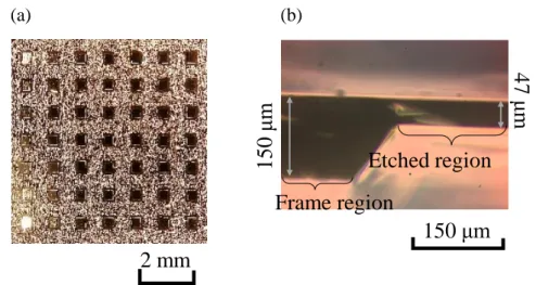
In this research, an aluminum photomask having different design was used for the patterning. There were 4 types of patterns: 1 x ϕ 6 mm, 4 x ϕ 4 mm, 9 x ϕ 2 mm, 49 x 500 x 500 µm2
. Finally, samples were dipped into developer (AZ 351B, Clariant) for 70 s and baked at 140°C for 15 min. As a result, a photoresist film with a thickness of about 2 µm could be formed on the SiO2 surface.
3. HF etching
The sample was continuously soaked in 5% HF until unmasked SiO2 was removed.
2.3 Fabrication process of partially-etched sensor plate
35 4. Protection wax
A glass plate was glued onto the Si3N4 surface by protection wax (KPW-A, Nikkaseiko) at 180°C to protect the sensor surface from the etchant.[28,29]
5. Anisotropic etching
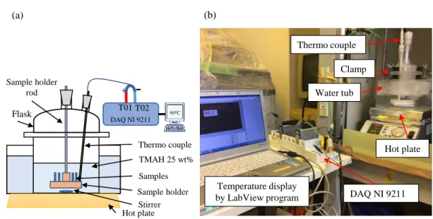
The sensor plate was then partially etched anisotropically in 25 wt.% tetramethylammonium hydroxide (TMAH) (Kanto Kagaku Co., INC) at a temperature of 90 ± 2°C.[28,50] The flask containing the etching solution was sunk into a hot water bath to minimize the deviation of the temperature as shown in Figure 2.5. The hot plate temperature was set to keep the inner solution at 90 ± 2°C. During the etching process, aluminum foil was used to wrap the flask to reduce the heat exchange.
Figure 2.6 shows the relation of etching time and etching depth. We can see the etching depth increases together with the etching time, and the etching rate was 42.3 µm/hour. In this research, the etching depth was about 150 µm to leave a remaining thickness of about 50 µm. The necessary etching time was 3.5 hours.
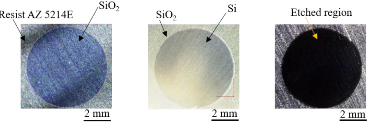
After etching, the sample was rinsed with xylene, acetone, ethylene, HF and deionized water to remove wax, SiO2 mask and other organic contaminations, respectively. Figure 2.7 shows the optical photos of a sample with 1 etched region ( ϕ 6 mm) after the lithography, HF etching and anisotropic etching. The etched region, which has black color, has the same shape as the resist pattern but the boundary between the etched and the frame region was inclined due to the different etching rates of silicon planes.
6. Evaporation of Au/Ti
Finally, thin layers of Au and Ti with the width of 1-1.5 mm were evaporated on two edges of the sample by physical vapor deposition to form the ohmic contacts.
2.3 Fabrication process of partially-etched sensor plate
36
Figure 2.5 (a) Apparatus used for anisotropic etching of Si by 25% TMAH at 90 ± 2°C and (b) the view of the etching set-up. To be safe, heating system including hot plate, water tub
and flask were put inside a fume hood.
Figure 2.6 Depth of the well as a function of the etching time. Hot plate Sample holder Samples TMAH 25 wt% Thermo couple Stirrer DAQ NI 9211 + T01 T02 90ºC Sample holder rod Flask Thermo couple DAQ NI 9211 Temperature display by LabView program Clamp Water tub Hot plate (a) (b)
Etching rate = 42.3 μm/hour
0
30
60
90
120
150
0
0.5
1
1.5
2
2.5
3
3.5
R
em
ai
ned
dept
h
(μ
m
)
2.4 Measurement method
37
Figure 2.7 Optical images of the back surface of a LAPS sensor plate (a) after forming a circular opening in the resist film by photolithography, (b) after removing SiO2 inside
the circular opening by 5% HF followed by removal of the resist film, and (c) after anisotropic etching of Si by TMAH.
2.4. Measurement method
⚫ Measurement system
The measurement system is used for modulation frequency lower than 10 kHz schematically shown in Figure 2.8. A bias voltage in the range of -3.0 V to +3.0 V is applied across the sensor plate with the help of a Ag/AgCl reference electrode (RE-1B, ALS Co., Ltd) and a multifunction I/O device (USB-6341, National Instruments). The collected signal is amplified with a current amplifier (LI-76, NF Corporation) and acquired bymultifunctional I/O device. For modulation frequencies higher than 10 kHz, the collected signal is amplified with a wideband current amplifier (AS-604F2, NF Corporation) and acquired by STEMlab125-10 (Red pitaya), which is able to acquire the signal at a sampling rate up to 125 MS/s as the schematic in Figure 2.9. The modulated light has a wavelength of 830 nm and is modulated at a frequency between 100 Hz and 300 kHz in the experiment of frequency characteristic.
2.4 Measurement method
38
Figure 2.8 Measurement system for modulation frequencies lower than 10 kHz.
Figure 2.9 Measurement system for modulation frequencies higher than 10 kHz (used in the measurement of frequency characteristics).
⚫ Evaluation of spatial resolution
In literature, there have been mainly two different ways of evaluating the spatial resolution of LAPS measurement. One of the methods to define the spatial resolution of a LAPS sensor is the evaluation of the object size that photocurrent image can visualize. The patterns with different sizes were formed on the sensing surface by photolithography. The patterns were
NI LabVIEW Laser 830 nm Reference electrode n-Si Electrolyte Data acquisition NI USB 6341 Vbias IAC FG DF1906 Si3N4/SiO2 Amplifier 106V/A NF, LI-76 Si3N4/SiO2 Laser 830 nm Reference electrode n-Si Electrolyte Data acquisition NI USB 6341 Vbias IAC FG DF1906 NI LabVIEW Data acquisition STEMlab 125-10 Wideband amplifier NF, AS-604F2
2.5 Experimental results
39
made from a thin layer of resist AZ 5214E with the thickness of 2 µm. A chrome mask with different lines and spaces with various widths of 10 µm, 20 µm, 30 µm, 50 µm, 100 µm, 300 µm was used. The sensing surface with different patterns was observed under optical microscope as shown in Figure 2.10. The sizes of the resist patterns were different from their sizes in the chrome mask due to error during the photolithography process.
Another spatial resolution evaluation is based on the lateral distance in which the photocurrent decays from 60% to 40% of the maximum value. In this case, a test pattern made of 50-μm-wide stripe made of resist AZ 5214E was formed on the sensing surface by photolithography. The solution used for these evaluations was pH 7 buffer (Titrisol, Merck).
Figure 2.10 Test pattern with different widths of resist stripes formed on the sensing surface of a partially-etched LAPS sensor plate.
2.5. Experimental results
2.5.1. Characteristics of the partially-etched sensor plate
The fabricated sensors with a size of 18 x 18 mm2 were fixed inside a sensor holder with the size of about 50 x 50 mm2 as shown in Figure 2.11. The sensing area was defined by a polydimethylsiloxane (PDMS) well structure on the sensor surface. The Au/Ti ohmic contacts were glued onto the metal plate by electroconductive silver paste (D-500, Dotite).
57 μm 326 μm 63 μm 13 μm 14 μm 13 μm 11 μm 101 μm 60 μm 63 μm 23 μm 13 μm 13 μm 11 μm 55 μm
2.5 Experimental results
40
The fabricated partially-etched sensor plate as shown in Figure 2.12 had totally 49 etched regions of about 500 x 500 μm2 within the sensing area of 10 x 10 mm2. An optical image of the back-side of the sensor plate is depicted in Figure 2.12(a). The thickness of the remained Si was 47 μm in the etched region and 150 μm in the frame region, as observed in the cross -section image at the boundary of the etched region and the frame region shown in Figure 2.12(b). The angle between the wall-surface (111) and the flat surface (100) is 54.7°. The thickness of the frame region was reduced from the initial thickness of 200 μm because the SiO2 mask was slowly etched and lost during the wet etching process. The shapes of some etched regions changed after the etching process, which might be attributed to the imperfect thickness uniformity of SiO2. Since Si3N4 can also be etched by TMAH, the Si3N4 front side of the sensor, which works as the sensing surface, was protected by a wax layer, so that the Si3N4 sensing surface was not etched. The pH sensitivity of the sensor plate was investigated to clarify the effect of the fabrication process.
Figure 2.11 Sensor holder for LAPS measurement. PDMS mold
Sensor holder
Metal Electrode