Author Cathal Cassidy, Hidehito Adaniya, Tsumoru Shintake
journal or
publication title
Journal of Applied Physics
volume 129
number 5
page range 055109
year 2021‑02‑04
Publisher AIP Publishing
Rights (C) 2021 Author(s).
Author's flag publisher
URL http://id.nii.ac.jp/1394/00001769/
doi: info:doi/10.1063/5.0036989
free path governing high-energy electron scattering in CdTe, via off-axis electron holography
Cite as: J. Appl. Phys. 129, 055109 (2021); https://doi.org/10.1063/5.0036989
Submitted: 09 November 2020 . Accepted: 14 January 2021 . Published Online: 04 February 2021
Cathal Cassidy, Hidehito Adaniya, and Tsumoru Shintake COLLECTIONS
This paper was selected as Featured
ARTICLES YOU MAY BE INTERESTED IN
Probing the phonon mean free paths in dislocation core by molecular dynamics simulation Journal of Applied Physics 129, 055103 (2021); https://doi.org/10.1063/5.0038265
Evidence of improvement in thermoelectric parameters of n-type Bi2Te3/graphite nanocomposite
Journal of Applied Physics 129, 055108 (2021); https://doi.org/10.1063/5.0030745 Clustering of oxygen point defects in transition metal nitrides
Journal of Applied Physics 129, 055305 (2021); https://doi.org/10.1063/5.0038459
Measurement and analysis of the mean free path governing high-energy electron scattering in CdTe, via off-axis electron holography
Cite as: J. Appl. Phys.129, 055109 (2021);doi: 10.1063/5.0036989
View Online Export Citation CrossMark
Submitted: 9 November 2020 · Accepted: 14 January 2021 · Published Online: 4 February 2021
Cathal Cassidy,a) Hidehito Adaniya, and Tsumoru Shintake AFFILIATIONS
Okinawa Institute of Science and Technology Graduate University, 1919-1 Tancha, Onna-son, Kunigami-gun, Okinawa 904-0495, Japan
a)Author to whom correspondence should be addressed:[email protected]
ABSTRACT
The mean free path governing the scattering of high-energy electrons in cadmium telluride (CdTe) has been measured and analyzed using off-axis electron holography (OEH). In the first part of the study, the total mean free path value was determined via acquisition and aggrega- tion of a large off-axis holography dataset at 300 kV and room temperature, yielding the valueλOEH¼52+7 nm. This is significantly shorter than some previously reported values obtained via different experimental techniques and theoretical calculations. To confirm the validity of the measurement and to understand the underlying physical scattering processes, the study was extended to systematically investi- gate the role of electron energy loss, electron scattering angle, and specimen temperature in the overall holography measurement.
This allowed the observed mean free path value to be clearly decomposed into terms of electronic (inelastic) and nuclear (elastic) scattering processes in the material and enabled direct measurement of the relevant contributions. Specifically, the determined attenuation coefficients wereμinel(ΔE.5 eV)¼5:9+1:2μm1andμel(ΔE,5 eV,α.3 mrad)¼13:5+1:2μm1 (full details in the main text). With appropriate consider- ation of the relevant scattering mechanisms, the mean free path value determined here from off-axis holography measurements is consistent with prior experimental measurements from other techniques and theoretical calculations. These insights and measurements should be of future value for quantitative holography and electron beam scattering experiments in CdTe.
© 2021 Author(s). All article content, except where otherwise noted, is licensed under a Creative Commons Attribution (CC BY) license (http://creativecommons.org/licenses/by/4.0/).https://doi.org/10.1063/5.0036989
I. INTRODUCTION
Cadmium telluride (CdTe) is a high-density compound semiconductor used in a variety of technological applications. In a high-resistivity single crystal form, as studied in this work, it has been used for many years as a detector in gamma-ray astronomy1–3 and recently is attracting interest for medical imaging.4A particular advantage of CdTe is direct high-energy photon detection with good stopping power, along with the ability to discriminate the photon-energies in a multi-source spectrum. Recently, CdTe has also been mentioned as a candidate material for direct electron detection,5 underpinning the need for deeper understanding of electron scattering processes in CdTe.
Electron holography is a well-established technique that allows the amplitude and phase of a specimen-transmitted electron wave to be quantitatively measured.6–8 Phase information is frequently the primary target of electron holography study, as it provides local
information on the electric and magnetic field distributions within the specimen, which is difficult to access via other means. For semiconductor specimens in particular, this allows high resolution mapping of electric potentials in functional devices.9,10Previously, we worked to determine the mean inner potential, V0, of CdTe, which is a fundamental, material-specific contributor to the elec- tron wave phase shift as it passes through the specimen.11
In addition to the phase, the electron wave amplitude is also acquired in a holography measurement and describes how the electron wave was locally attenuated upon interaction with the specimen, relative to a reference vacuum wave. This attenuation can be described via a material-specific mean free path parameter.
Knowledge of this parameter for a given material has a significant practical use, in that it allows the specimen thickness to be directly mapped using amplitude data, conveniently and in perfect registry with the simultaneously acquired phase data.12,13
Furthermore, quantitative study of the amplitude signal can also yield some fundamental insights into the specific scattering pro- cesses occurring in the specimen. Measurement and interpreta- tion of the mean free path in CdTe, as measured in off-axis holography at 300 kV, is the topic of this paper.
II. THEORY
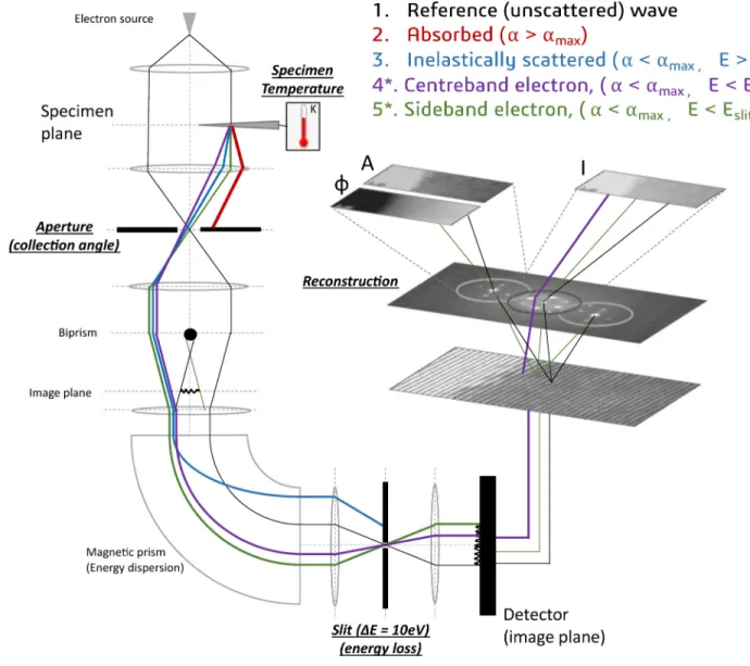
The theoretical background for off-axis electron holography is well-documented, with numerous comprehensive treatments in the literature. For example, see comprehensive reference textbooks14–16 and more recent reviews.17–23A short summary of pertinent points follows, while an overview of the acquisition and reconstruction process is shown inFig. 1.
Assuming that dynamical diffraction effects can be neglected (low-index crystal zone axes are avoided), upon propagation through the specimen, electron wave amplitudeA(x,y) and phase shiftΔf(x,y) are given by15
A(x,y)¼A0e2λOEHt(x,y), (1)
Δf(x,y)¼cEV0t(x,y)þcE
ðþ1
1V(x,ye h
ðþ1
1Az(x,y) dz: (2) Each parameter is briefly defined here, while additional details are also provided in thesupplementary material.A0is the amplitude of the reference electron wave that passed through vacuum.t(x,y) is the thickness of the specimen.λOEH is the mean free path govern- ing electron scattering. As the value of this parameter is directly tied to the holographic acquisition and reconstruction process, we explicitly identify it with the subscript OEH (Off-axis Electron Holography).cEis an interaction parameter that depends upon the velocity of the beam electron.V0is the mean inner potential of the material, arising from the net contribution of the positive field of the nuclei and the partial screening by the negative field from the electron clouds. V(x,y) is an electrostatic potential term, which arises if there is any extra net potential from factors such as charg- ing or external bias applied to the material. As such fields may extend over quite large regions outside the specimen, the integral must be performed overz(the beam direction).eis the electronic charge andhis the Planck constant divided by 2π.Az(x,y) is the z-component of magnetic vector potential, arising from any mag- netic fields, if present.
Both the amplitude and phase signals depend directly upon the specimen thickness, t(x,y); therefore, accurate and reliable thickness measurement is a necessary prerequisite before more complex analyses can be undertaken. There are also two material- specific terms, V0 in the phase term and λOEH in the amplitude term, which must be known before progressing to more complex quantitative holography studies of a specific material. We have pre- viously reported on the mean inner potential parameter11and in this work turn our attention to the mean free path.
λOEH is a mean free path parameter describing the reduction of the electron wave amplitude upon traversing the specimen.12 It can alternatively be expressed as an attenuation coefficient, μ¼1=λ, which is entirely equivalent, but this notation can
sometimes be more convenient (e.g., if contributions from several different absorptive processes, to the total attenuation, are being added). Note that in considering mean free paths, the pertinent scattering processes and experimental conventions differ from tech- nique to technique, and in that context, we explicitly identify this parameter as λOEH (Off-axis Electron Holography). This is an important point, and we tabulate and relate some different defini- tions ofλin various techniques of relevance in thesupplementary material. We will also discuss this topic further in Sec.IV.
Equations(1)and(2)can be re-arranged, and assuming there are no external electric or magnetic fields present in the specimen under study, the mean free path can be expressed in terms of the amplitude and phase signals as
λOEH¼ t(x,y) 2 ln [A(x,Ay)
0 ]¼ Δf(x,y)
2cEV0ln [A(x,Ay)
0 ]: (3)
To calculate the mean free path from experimentally acquired data, the first expression in Eq.(3), which does not depend on the phase, can be employed when the specimen thickness is known from other means [for example, from a geometrically well-defined (cleaved) sample, diffraction measurement or EELS mapping]. The second form in Eq. (3), which does include the experimentally acquired phase data, can be utilized if it is assured that dynamical diffraction and external field effects are absent, and the mean inner potentialV0is reliably known. We have primarily relied upon the latter method for mean free path calculation but also performed some reference EELS measurements to confirm the reliability of the thickness values. Note that we have neglected any microscope lens magnetic field contribution in deriving Eq.(3), as the CdTe speci- men is not magnetic and, therefore, will not exhibit any significant magnetization in response to an external magnetic field. Any inho- mogeneity arising from the fields from the microscope optical com- ponents will be corrected via the process of normalization with an empty (without specimen) reference hologram, which was per- formed in all cases. Therefore, in this work, we have used both the TEM mode (with objective lens on and lens magnetic field present) and the Lorentz mode (with objective lens off and the specimen in a nominally field-free condition). The amplitude measurements are mutually consistent from both of these modes, as will be described in detail in the discussion ofFig. 5later.
III. EXPERIMENTAL
Single crystal CdTe specimens were purchased from Acrorad Ltd (Okinawa, Japan). These crystals are detector-grade, high- resistivity single crystals fabricated using the traveling heater method.24 Electron transparent lamellae were fabricated using Focused Ion Beam (FIB), with various wedge and needle geome- tries.11Samples were prepared using sequential 30 kV, 8 kV, and 2 kV Ga ion milling for bulk, intermediate, and fine polishing, respectively. Specimens were oriented perpendicular to the h110i zone axis, with h111i surface normal. Samples were milled using ThermoFisher Helios G3 UC and Hitachi DMF400025instruments.
Typically, 1–2nm of surface amorphization was observed on the CdTe specimen sidewalls (Fig. S1 in the supplementary material).
Within the crystal, dislocations were observed quite frequently
(Fig. S2 in thesupplementary material), as previously reported for this material,26and such areas were avoided for the detailed holog- raphy measurements reported in the paper. Note that additionally, one wedge specimen was prepared with intentionally high acceler- ating voltage and beam current to result in complete amorphization of the material. This specimen was prepared to help evaluate how specimen crystallinity and dynamical scattering fluctuations
affected the measurement (as discussed in Sec. IV). An image of this specimen is shown in Fig. S3 of thesupplementary material.
Electron holography acquisitions were performed in a ThermoFisher Titan G2 electron microscope, operated at 300 kV.
This microscope was equipped with a Schottky XFEG electron source, S-TWIN objective lens (with collection half-angles, α, in the range of 2.6–75 mrad), Lorentz lens (with collection half-angles FIG. 1. Illustration of the off-axis holography acquisition and reconstruction process. (a) Schematic for standard off-axis electron holography. (b) Experimental hologram (inset: zoom of biprism interference fringes in the vacuum region). (c) Fast Fourier transform of the acquired hologram, showing the centerband (CB) and conjugate side- bands (SB, SB*). The electron wave amplitude and phase are recovered by masking and inverse Fourier transform of either of the sideband distributions. The centerband region can also be reconstructed to yield a conventional intensity image. (d) and (e) Amplitude and phase maps, reconstructed by masking and inverse Fourier transform of one of the sidebands. The equations underlying these signals (valid for weakly diffracting conditions and in the absence of external fields) are also shown. There are two material-specific parameters: mean inner potential,V0(determined in our previous work11) and mean free path,λOEH(the subject of this paper).
in the range of 2.1–10 mrad), image Cs-corrector (CEOS GmbH), a single electrostatic biprism in the selected area plane, and a post- column Gatan Quantum 966 energy filter, with Gatan 2 k2 k UltrascanXP1000 cameras located before and after the energy filter, respectively. A double-tilt heating holder (Gatan 652) and a single tilt cooling holder (Gatan 613) could be employed for executing experiments at elevated or reduced temperatures. This hardware was capable of a biprism fringe contrast of 30% and phase and amplitude resolutions of 2π=550 radians (11 mrad) and 0:9%, respectively (standard deviation of the averaged reconstructed signals in vacuum areas). This represents best case conditions in vacuum—real specimen acquisition parameters were typically worse than this.
Numerical reconstruction was performed using Gatan Holoworks V5 and V6,27along with self-written Digital Micrograph scripts prepared for specific analyses. The Hologram class of the Hyperspy28 Python package was also utilized, particularly for han- dling of large image stacks.
IV. RESULTS AND DISCUSSION
A. Simple measurement of the total mean free path In this section, a straightforward measurement of the mean free path will first be presented, without consideration of the underlying processes that govern the value. Examples of amplitude and phase data will be shown, and the computation of mean free path values, via aggregation of a large data set from CdTe and other reference materials, will be presented.
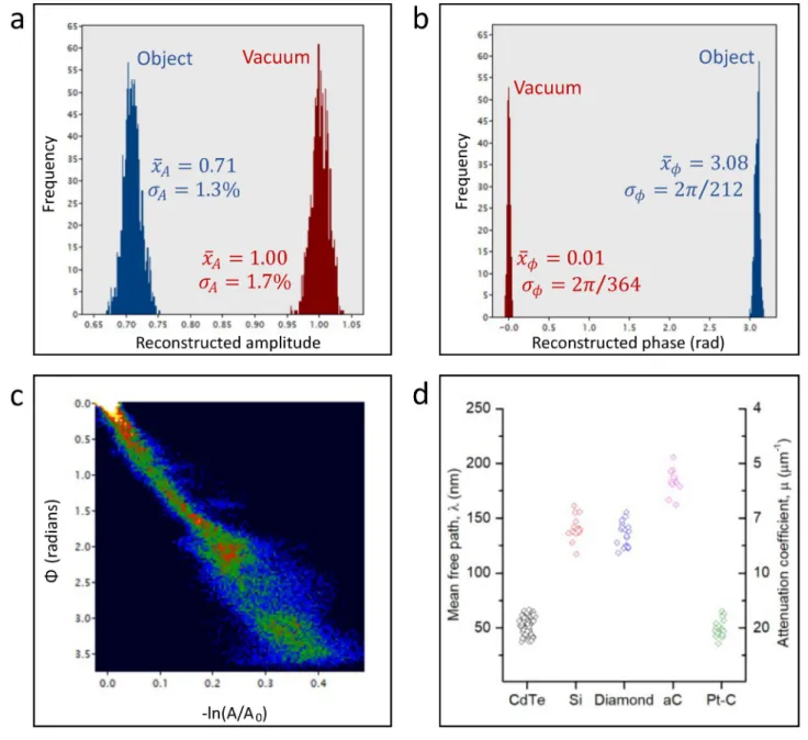
InFigs. 2(a)and2(b), we show the distributions of amplitude and phase obtained from a defined region of interest on a CdTe specimen. These particular data were generated via averaging of 1000 individual hologram frames, each with an exposure time of 1s. As shown in the figure, the data show standard deviations in A and Δf of 1.3% and 2π/212 radians (30 mrad) in the specimen area, respectively. For practical reasons, we acquired such large data stacks only on a sample basis, and usually, used smaller image stacks with higher noise (dataset D1 in thesupplementary material includes details for all CdTe acquisitions).
InFig. 2(c), we show an example bivariate histogram, combin- ing amplitude and phase data from an extended field of view. Such bivariate histograms were very helpful visualizing the relationship between amplitude and phase data29and filtering any anomalous regions that should be excluded from the measurement (such as strongly diffracting regions in proximity to a dislocation or carbon contamination regions). Such amplitude and phase data can then be utilized directly in Eq.(3)to compute the mean free path.
The variability from measurement to measurement, with dif- ferent specimens, experimental settings, and reconstruction param- eters, was of greater concern than the precision of individual measurements (which could be refined by straightforward, but laborious, integration of more frames). With this in mind, a large number of measurements were acquired with different experimen- tal parameters—different specimen geometries, locations, tilts, thicknesses, magnifications, biprism voltages, and reconstruction settings. The results of all CdTe mean free path measurements are summarized in Fig. 2(d), and the acquisition conditions for each individual data point are tabulated in dataset D1 of the
supplementary material. In general, the majority of the measure- ments fell within a well-defined range, from about 40 to 60 nm, as a function of variations in experimental parameters. The only exception to this was the case when the specimen was tilted close to a strongly diffracting, low-index zone axis, as expected.31–33 In that case, the measured values were quite anomalous and easily distinguished from the main population (and were excluded from the analysis).
In general, the topic of dynamical scattering in the crystal is central to this work and poses some risk to the validity of the measurement. With this concern in mind, aside from using many different thicknesses and tilts, we also deliberately prepared one amorphous CdTe sample, with a view to having a sample with maximal disorder and minimal dynamical scattering related fluctu- ations. The measurements from the amorphous sample fell within the main distribution shown inFig. 2(d), matching the acquisitions from the off-zone axis crystalline specimens, and indeed have already been included in the figure and data analysis. From an experimental and practical point of view, we believe that this is a reasonable way to validate that the measurements are reliable and are not grossly affected by erratic dynamical scattering fluctuations.
Thus, we believe that the reported value can be reliably utilized by others in the field for specimen thickness mapping.
From a more fundamental theoretical perspective, the topic of dynamical scattering is rather complicated. This topic has been treated in detail by Lubket al.31for mean inner potential of Si and Au, providing a very clear insight into the complexity of the problem, the magnitude of possible effects, and the effect of experi- mental parameters such as accelerating voltage and specimen tilt.
To our knowledge, such a detailed study has not been performed to date for CdTe and is beyond the scope of the current work. It is our strong wish to perform such a dedicated simulation study for CdTe in future. Notwithstanding this underlying theoretical com- plexity, we still believe that experimental approach of averaging over multiple (far from zone axis) tilts, thicknesses, and amorphous sample measurements is valid, and the determined value, with associated errors, is general and reliable.
We also performed reference measurements on a number of other common materials (C, Si, Pt) to ensure the reliability of the experimental measurement. While published values for these materials with comparable experimental settings are limited, these values agree reasonably well with available prior values (for example, λOEH,Si,200 kV¼120 nm9 and λOEH,C,100 kV¼55 nm34) and with general expectations in terms of material atomic number and density.
Based upon the aggregated results shown in Fig. 2(d), representing all of the valid CdTe measurements, we report a mean free path value for CdTe at 300 kV of λOEH¼52+7 nm (mean and standard deviation of all valid measurements). This simple measurement of the mean free path for CdTe is already of some benefit, as it allows straightforward measurement of specimen thickness to facilitate more complex quantitative holography studies.
However, this value is significantly shorter than the CdTe mean free path published previously from 300 kV electron energy loss spectroscopy (EELS) measurements: λEELS¼192+10 nm11 and also prior theoretical calculations,35provoking curiosity about the reasons for the large difference. Given the experimental complex- ity, there are certainly risks of artifacts or unforeseen equipment-
dependencies. Furthermore, there are numerous electron scattering processes in the background that might play some role in the holog- raphy measurement (such as very low-loss phonon scattering events and the finite possibility of interference of inelastically scattered waves36–40), but whose contribution was poorly understood. While a
comprehensive analysis of these rather complex topics is beyond the scope of this paper on CdTe, it was nevertheless prudent to confirm the experimental robustness of the obtained holography data and also more generally understand the critical factors that significantly influence the experimental off-axis holography results.
FIG. 2.Amplitude, phase, and mean free path data. (a) and (b) Experimental measurement of CdTe amplitude and phase, respectively. Data from 1000 individual holo- grams have been averaged to produce the shown distributions, extracted from local regions of interest on object and vacuum regions. (c) Bivariate histogram showing the relationship between the acquired amplitude (log) and phase distributions over an acquired frame including vacuum and varying specimen thickness regions. Such visual- izations are helpful for correlating the amplitude and phase signals, assessing acquisition quality and identifying anomalous regions. (d) Calculated mean free path for CdTe, derived from experimental data acquired in a range of different experiments (different specimens, thicknesses, tilts, biprism voltages, magnifications, integration times, reconstruction parameters). Note that we also performed brief reference measurements on single crystal silicon (“Si”), polycrystalline diamond30(“Diamond”), amor- phous carbon (“aC”), and a platinum-carbon mixed phase layer (“Pt-C”).
B. Further analysis of the mean free path
With this in mind, the study was extended to explore the material-specific and equipment-specific factors underpinning the total mean free path values that we reported inFig. 2. It is relatively straightforward to investigate the effect of specific parameters in a systematic way, using standard operating modes and adjustable components on the microscope.
An overview of the varied experimental parameters is shown inFig. 3. By varying the microscope objective aperture in the back focal plane, it was possible to vary the collection angle of the
optical system and thereby quantify the relationship between angle of scattering and the reconstructed amplitude signal. By employing an energy filter, it was possible to remove electrons that had experi- enced a large (experimentally resolvable) energy loss in the specimen and thereby quantify how such electrons contribute to the hologram.
In this work, a slit width of 10 eV was employed, centered at the zero-loss position, meaning that electrons with an energy loss.5 eV could be excluded from the hologram formation process. Energy losses in this range are related to electronic scattering events (such as plasmon, interband, and core electron excitation). Very low energy
FIG. 3. Schematic overview of the experimental system, with an illustration of how various different scattering processes contribute to the mean signals reconstructed from the hologram. The scattering angle dependence (described by half-angleα) could be explored by varying the objective aperture in the back focal plane. The energy dependence could be investigated by insertion of the energy filtering slit. The specimen temperature could also be varied. The factors governing the off-axis holography mean amplitude signal could also be investigated by comparing the numerical reconstructions produced from the centerband and sideband distributions. *The details regarding populations 4 and 5 will be clarified in the discussion ofFig. 5.
with this experimental configuration. The specimen temperature could also be varied. As the mean free paths associated with some nuclear (phonon, thermal diffuse) scattering processes are expected to show a very strong variation with temperature (2–4 x, from 0 K to 300 K),41,42it was of interest to evaluate how the electron holography measurement was affected by changes in the specimen temperature and thereby gain some insight into the role played by such processes.
Furthermore, by also reconstructing the signal in the hologram centerband (CB) in addition to the usual hologram sideband (SB), as shown in the hologram FFT, we can gain further insight into the mechanisms at play. The image arising from reconstruction of the centerband is similar to a conventional intensity image, in that it does not directly filter inelastically scattered or incoherent electrons—all scattered electrons which make it through the aper- tures will contribute to the image. The hologram sideband, which is used to extract the wave amplitude and phase, on the other hand, by definition is formed purely by interference of the object and reference waves, and as a result, any signal reconstructed from the sideband will be highly sensitive to the coherence of the interfering electrons and the details of the resultant interference pattern. Thus, comparison between the two cases is quite useful, and the fact that both signals are acquired automatically in the same experiment, with the same parameters and in perfect registry, allows a very direct and reliable comparison to be made.
There are a few important points to note about utilizing the data available from the centerband, however. While the centerband reconstruction is very similar to a standard image, the presence of the biprism means that there is an extra intensity contribution from the vacuum reference wave, which affects the apparent contrast. Furthermore, while sideband reconstruction directly yields an amplitude signal, both conventional imaging and cen- terband reconstruction yield intensity (amplitude squared) terms. Such differences, while not presenting a major problem to the analysis, must nevertheless be carefully handled to ensure that a valid comparison can be made. Details are summarized in the supplementary material. Note that we occasionally use the shorthand
“inelastic/elastic”and“electronic/nuclear”terms to differentiate scat- tering events with energy losses greater or less than 5 eV, respectively, as is commonly done in the literature, but this is obviously an over- simplification of the actual scattering phenomena that are occurring.
Figure 4 shows some example data to illustrate how the various signals vary, whileFig. 5shows a highly distilled summary of the key findings of a wide ranging investigation.
As mentioned, for illustrative purposes, Fig. 4shows a com- parison of some selected acquisitions—specifically reconstructed centerband and sideband images with and without energy filtering (at room temperature, with a collection half-angle of 75 mrad).
The acquired signals have been adjusted (as outlined in the supplementary material) such that they are both expressed in terms of electron wave amplitude and are directly comparable. The colored boxes in each image indicate the electron types that are presumed to be contributing to the image, with reference to the beam paths shown inFig. 3. These are included for illustrative pur- poses only—the details will be clarified in the discussion ofFig. 5.
First, in comparison with the centerband and sideband data in Fig. 4, it is clear that the sideband images show significantly higher
consistent with expectations, as any inelastically scattered/incoher- ent electrons should be included in the centerband but rejected from the sideband. Second, it is clear that the centerband image signal is significantly reduced by insertion of the energy filter, as expected, given that the energy filter removes inelastically scattered electrons that would otherwise have been included in the image.
Finally, for the case of the sideband images, it is clear that the reconstructed amplitude signal is not significantly affected by the insertion of the energy filter. This indicates that those electrons with energy losses greater than 5 eV do not make it into the reconstructed amplitude signal anyway, having lost coherence with the main ensemble; therefore, inserting the filter has no discernible effect. The general story seems to be consistent with expectations, and we can proceed to a more quantitative analysis of the respective signals.
InFig. 5, we show a summary figure that encapsulates all of our measurements over collection angles, energy filtering, and specimen temperature, with corresponding data extracted from reconstructed sidebands, reconstructed centerbands, and conven- tional (non-holographic) images acquired with the biprism retracted.43These experiments have been executed multiple times, with different microscope set-ups and specimen materials, with consistent results. The attenuation coefficient (μ) notation has been utilized here, as it allows a more directly intuitive approach than adding reciprocals (mean free paths). Figures 5(a)and5(b) show investigations performed in a standard TEM mode, with the objective lens on. This mode has the advantage of a well-defined collection angle, which can be varied over a large range, but has drawbacks in terms of field of view and fringe contrast, with asso- ciated limitation for signal to noise.Figure 5(c)is a similar mea- surement to Fig. 5(a)but performed in a Lorentz mode with the objective lens switched off. This optical mode has a severe restric- tion on the available collection angle but has the advantage of allowing wider fields of view and higher signal-to-noise measure- ments, thus complementing prior TEM-mode measurements.
ConsideringFig. 5(a), there are two central findings to high- light. First, the hologram sideband-derived signal did not vary sig- nificantly, within our measurement error, as a function of changes in both energy filtering and collection angle. That the sideband signal is not affected by the insertion of the energy filter is reason- ably in line with expectations, but the absence of a strong depen- dence on the collection angle is more intriguing. This lack of sensitivity to the collection angle has been reported previously34 but also seems to differ slightly from some more recent work.44,45 Given the differences in complex experimental setups, it may be that both measurements are mutually compatible within the associ- ated experimental errors. For our specific setup, the experiment was repeated several times with different parameters and materials, and the behavior was reproducible. Second, as expected, the center- band signal did directly depend upon energy filtering and collection angle and, most interestingly, converged to match the sideband signal in the limit of the filtered, small-angle condition. This conver- gence is also confirmed in Fig. 5(c) in a rather different optical mode. Together, these observations provide strong evidence that the total attenuation coefficient we have measured for CdTe in off-axis holography, which is derived from the mean amplitude signal, is a sum of the inelastic scattering term, plus the elastic scattering out of
the direct beam. More specifically, the mean attenuation observed in the CdTe off-axis electron holography amplitude measurements is a sum of (i) electronic, inelastic scattering contribution (ΔE.5 eV) and (ii) the elastic (ΔE,5 eV) scattering outside the direct beam (α.3 mrad), via Rutherford-type scattering on the screened nuclear potential. This is quite interesting and may provide a val- uable insight for reliably relating the scattering behavior observed in different experimental techniques to the underlying material properties.
First, we discuss the underlying mechanisms. Regarding inelastic scattering, μinel(ΔE.5 eV), electrons that have undergone a large (.5 eV) inelastic scattering event will presumably have lost coherence with the main ensemble and thus do not contribute to the mean reconstructed value. Some prior work has demonstrated the possibility of interference of inelastically scattered electrons, for example,39,46,47 but we did not note any detectable contribution within our attenuation coefficient measurements. This is in line with expectations.
Regarding the attenuation term arising from elastic scattering outside the direct beam, μel(ΔE,5 eV,α.3 mrad), this is less obvious.
Clearly, electrons that have been scattered to higher angles ulti- mately contribute to the mean signal of the centerband but are rejected from the mean signal of the sideband. There are several mechanisms that might play a role, such as loss of coherence owing to low-energy loss (phonon) scattering or damping of the acquisi- tion of higher frequency signals. However, we suggest that the observed behavior can be explained more simply as being a direct consequence of the utilized holography process, without a need to explicitly consider specific electron scattering or acquisition factors.
A short summary follows. In the off-axis hologram, the dominant oscillating fringe pattern and the associated dominant sideband carrier frequency in the Fourier space is produced by interference between the vacuum reference wave and the object forward-scattered (000) beam. This dominant carrier frequency is then deliberately selected and centered in the Fourier space during reconstruction. Upon inverse transformation, this component, FIG. 4. Illustration of the effect of electron energy-loss filtering on the hologram centerband and sideband-derived amplitude images, with corresponding line profiles. The centerband acquisitions have been processed such that they yield an amplitude signal, which can be directly compared with the sideband data. Without filtering, the center- band exhibits a small decrease in the signal in the object region relative to the adjacent vacuum, which is related to scattering-absorption (75 mrad aperture radius). Upon insertion of the energy filter (at position 0 eV and width 10 eV), the centerband signal reduces significantly. This is attributed to the filtering of high-energy loss electrons (.5 eV) and is assumed to be dominated by plasmon scattering. Considering next the sideband amplitude data, the object region signal is significantly reduced in compar- ison with the centerband case, resulting in stronger image contrast. Insertion of the energy filter has no discernible effect on the sideband reconstructed amplitude (indicat- ing that the interference and holographic reconstruction intrinsically rejects the inelastically scattered electrons anyway). The colored squares correspond to the associated beam paths inFig. 3(for illustrative purposes only, the details will be clarified in the discussion ofFig. 5).
arising from the (000) beam, uniquely defines the mean of the reconstructed amplitude signal. Interferometric terms at other fre- quencies (arising from interference of beams scattered at other angles) may also appear in the sideband and be transferred into the reconstructed amplitude image but add only oscillating terms (reso- lution) to the reconstructed amplitude image. This behavior intrin- sically differs from conventional imaging, in which the scattered beams do contribute directly to the mean signal at the time of acquisition on the detector, irrespective of their scattering angle.
A deeper discussion is beyond the scope of the current paper, but it is our intention to prepare a follow-up paper to explore this topic in further detail. Within the scope of the current paper on CdTe, this description seems to provide a reasonable explanation of the observed experimental results.
At this stage, we may revisit the previous electron ray paths shown schematically inFig. 3. Based on the results inFig. 5, popu- lation 4 can be identified as those electrons that have been elasti- cally scattered outside the direct beam (thus contributing to the centerband mean amplitude values but not the sideband mean values), while population 5 is the direct, forward-scattered (000) beam (which contributes to both the centerband and sideband mean amplitude values). It must be highlighted, in strong terms, that this description is only relevant for describing mean signals extracted from the amplitude images, in the context of computing
mean free paths, and does not accurately reflect the general transfer of information or resolution through the system.
Next, we consider the specific values of these distinct attenua- tion mechanisms, which in general will be highly specific to the material under study. The inelastic contribution will depend upon the electronic band structure, in a similar fashion to EELS,48while the elastic contribution will depend directly upon the atomic number of the specimen nuclei. Thus, for a low-Z material like carbon, it might be expected that the elastic scattering contribution might be relatively small, and the EELS and holography derived attenuation coefficients might be similar. However, for a high-Z material, the nuclear scattering term could be very significant, and the attenuation coefficient derived from holography might be significantly larger than that from EELS. For CdTe specifically, we can directly extract the actual values of the respective attenuation coefficients from Fig. 5. The inelastic scattering contribution can be determined from the increase in the centerband-derived attenu- ation coefficient, upon insertion of the energy filter. This term must also vary with the collection angle, especially at low angles (plasmon scattering is strongly forward peaked) but should satu- rate at larger angles as a relatively low proportion of energy-loss electrons are excluded by the aperture in this angular range.
As can be seen in Fig. 5(a), this is indeed the case—the offset between filtered and unfiltered traces is relatively constant at higher FIG. 5.The effect of electron energy-loss filtering, collection angle, and specimen temperature upon the CdTe attenuation coefficient, as evaluated from both centerband and sideband reconstructions, as well as conventional intensity images. (a) Data acquired with the objective lens on (TEM mode), with good control over the collection angle but rel- atively poor field of view and signal-to-noise performance. (b) Effect of the specimen temperature upon the reconstructed centerband and sideband. (c) Counterpart to (a), using the Lorentz mode that allows a wider field of view and better signal-to-noise performance but which has limits on the available collection angle. A key finding is that the sideband signal does not change significantly as a function of energy filtering and collection angle. The centerband signal does vary quite strongly with these parameters, as expected, and interestingly, in the limit of energy filtering and small collection angle, converges upon the sideband signal. It is also notable that the signals do not show very large changes, at least relative to our measurement sensitivity, over a temperature change from 93 K up to 473 K, which is discussed further in the main text. The symbols, colors, and y-axes are consistent across all three plots, and the legend shown within the plot area inFig. 5(c)also applies toFigs. 5(a)and5(b).
angles. With this approach, we obtain a value of 5:9+1:2μm1 (which is consistent with our prior EELS measurements11and also prior theoretical calculations,35 keeping in mind the subtle differ- ences in definition, summarized in thesupplementary material). The remaining attenuation can then be assigned to the elastic scattering term, yielding a value of 13:5+1:2μm1. This indicates that for CdTe, the elastic scattering on the screened field of the nuclei is a significantly bigger contributor, than the inelastic (electronic) scatter- ing term, to the total attenuation observed in off-axis holography.
This is reasonable given the high density and atomic number of the material. Indeed, a simple Rutherford scattering calculation,45while not providing a rigorous and quantitative value, nevertheless provides some guidance on the expected order of magnitude. Such a calcula- tion yields a calculated attenuation coefficient value of 17.2μm1for CdTe (see the supplementary material; corresponding values for carbon and silicon are 3.7μm1 and 5.1μm1, respectively).
Thus, while the Rutherford scattering estimate does not perfectly match the experimental measurement, it is certainly of the correct order of magnitude, and it seems that the relatively high contribu- tion arising from elastic scattering in CdTe is reasonably in line with expectations.
The temperature dependence of the holography amplitude signal was also investigated, as shown inFig. 5(b). Our motivation in performing this study was that some electron scattering pro- cesses, such as phonon or TDS scattering, are reported to show a very strong thermal dependence.41,42Specifically for CdTe, Allen and Rossouw42 predicted that the CdTe mean free path for TDS scattering would decrease by a factor of three, from approximately 300 nm to 100 nm, upon changing the temperature from 0 K to 300 K. Against this background, it was of interest to ascertain if our measured value of the CdTe attenuation coefficient was particularly sensitive to the temperature of the specimen. However, in summary, changes on the order of a factor of two or three, as a function of temperature, were not observed, as shown inFig. 5(b).
Certainly, the attenuation coefficient derived from the recon- structed sideband signal appears to increase slightly as a function of temperature (and this behavior is worthy of further dedicated study), but the change is on the order of our experimental accuracy in the current work, and large shifts, by a factor of two or three, were certainly not detected. For the present paper, in documenting the mean free path for CdTe, the temperature of the specimen does not seem to be a major factor in modulating the amplitude signal within our experimental errors. More generally, the thermal depen- dence of scattering by the lattice is a highly interesting but rather complex topic and is certainly worthy of more precise and in-depth measurements in future.
Finally, it is important to flag some specific characteristics and limitations of this study, which might limit the generality of the results. Only one electron biprism was available in the microscope, which constrained the available field of view and achievable fringe contrast for holography measurements, with associated limits of achievable signal to noise. Furthermore, use of a single biprism pre- cluded large spatial separation of object and reference wave regions, which might result in some finite cross-talk between the two regions, particularly for high-angle scattered electrons or for highly delocalized phenomena such as phonon excitation; therefore, the results should be interpreted with care. We analyzed crystals
,100 nm thick in this work, given the rather short mean free path;
therefore, the conclusions may not hold in studies of thicker crys- tals. We did not consider the effects of optical aberrations on high- angle scattered electrons. For the temperature study, the nominal holder temperature was reported, but the actual local temperature at the specimen was not verified, and it may conceivably have dif- fered significantly from the reported value. Future work would benefit from studies with higher performance multiple-biprism holography microscopes,49,50 consideration of thicker samples (perhaps with a higher acceleration voltage49), local verification of specimen temperature (e.g., via EELS51), and higher energy resolu- tion electron energy loss spectrometry capability.52
V. CONCLUSIONS
The primary finding of this work is a measurement of the mean free path governing electron wave attenuation in CdTe, as λOEH¼52+7 nm (in off-axis electron holography measurement at 300 kV). Under comparable experimental conditions, this value can be directly utilized for convenient specimen thickness mapping in CdTe. We have also attempted to decompose the individual compo- nents underlying this measured value and suggest that the observed mean amplitude attenuation can be reasonably explained by the sum of electronic inelastic scattering (plasmon and core-loss,ΔE.5 eV), with an attenuation coefficient of μinel(ΔE.5 eV)¼5:9+1:2μm1, and nuclear elastic scattering out of the forward-scattered beam (ΔE,5 eV,α.3 mrad), with an attenuation coefficient of μel(ΔE,5 eV,α.3 mrad)¼13:5+1:2μm1. These results will hopefully be a useful foundation for future, more quantitative holography studies of CdTe intrinsic material parameters and functional device potentials.
SUPPLEMENTARY MATERIAL
See thesupplementary materialthat contains additional detail on definition of parameters in Eqs. (1)and (2), definition of the mean free path/attenuation coefficient in different techniques, further specimen preparation information, CdTe attenuation coeffi- cient estimation based on a simple Rutherford scattering model, and further details on CdTe experimental acquisition settings.
ACKNOWLEDGMENTS
This work was supported by JSPS Kakenhi (Grant No.
18KO4247), “Electron holography studies of CdTe.” The authors would like to thank Dr. Edgar Völkl for frequent support for numerical reconstruction issues. The authors thank Dr. Ken Harada, Professor Marek Malac, and Professor Jun Yamasaki for helpful feedback on multiple manuscript drafts. The authors would also like to thank Dr. Stoffel D. Janssens and Dr. Alessandro Giussani (Mathematics, Mechanics, and Materials Unit, OIST) for provision of the specimen with polycrystalline diamond, amor- phous carbon, and single crystalline silicon layers, utilized for refer- ence measurements.
DATA AVAILABILITY
The data that support the findings of this study are available from the corresponding author upon reasonable request.
1T. Takahashi, K. Hirose, C. Matsumoto, K. Takizawa, R. Ohno, T. Ozaki, K. Mori, and Y. Tomita,“Performance of a new Schottky CdTe detector for hard x-ray spectroscopy,”Proc. SPIE3446, 29–37 (1998).
2S. Takeda, H. Aono, S. Okuyama, S.-N. Ishikawa, H. Odaka, S. Watanabe, M. Kokubun, T. Takahashi, K. Nakazawa, H. Tajimaet al.,“Experimental results of the gamma-ray imaging capability with a Si/CdTe semiconductor Compton camera,”IEEE Trans. Nucl. Sci.56, 783–790 (2009).
3C. Matsumoto, T. Takahashi, K. Takizawa, R. Ohno, T. Ozaki, and K. Mori,
“Performance of a new Schottky CdTe detector for hard x-ray spectroscopy,”
IEEE Trans. Nucl. Sci.45, 428–432 (1998).
4S. Procz, G. Roque, C. Avila, J. Racedo, R. Rueda, I. Santos, and M. Fiederle,
“Investigation of CdTe, GaAs, Se and Si as sensor materials for mammography,”
IEEE Trans. Med. Imaging39, 3766 (2020).
5B. Plotkin-Swing, G. J. Corbin, S. De Carlo, N. Dellby, C. Hoermann, M. V. Hoffman, T. C. Lovejoy, C. E. Meyer, A. Mittelberger, and R. Pantelic,
“Hybrid pixel direct detector for electron energy loss spectroscopy,”
Ultramicroscopy217, 113067 (2020).
6A. Tonomura,“Applications of electron holography,”Rev. Mod. Phys.59, 639 (1987).
7H. Lichte, P. Formanek, A. Lenk, M. Linck, C. Matzeck, M. Lehmann, and P. Simon,“Electron holography: Applications to materials questions,” Annu.
Rev. Mater. Res.37, 539–588 (2007).
8M. R. McCartney and D. J. Smith,“Electron holography: Phase imaging with nanometer resolution,”Annu. Rev. Mater. Res.37, 729–767 (2007).
9D. Cooper, “Off-axis electron holography for the measurement of active dopants in silicon semiconductor devices,” J. Phys. D: Appl. Phys.49, 474001 (2016).
10S. Anada, K. Yamamoto, H. Sasaki, N. Shibata, Y. Hori, K. Kinugawa, A. Imamura, and T. Hirayama,“Precise measurement of electric potential, field, and charge density profiles across a biased GaAs p-n tunnel junction byin situ phase-shifting electron holography,”J. Appl. Phys.122, 225702 (2017).
11C. Cassidy, A. Dhar, and T. Shintake, “Determination of the mean inner potential of cadmium telluride via electron holography,”Appl. Phys. Lett.110, 163503 (2017).
12M. McCartney and M. Gajdardziska-Josifovska,“Absolute measurement of normalized thickness, t/λi, from off-axis electron holography,”Ultramicroscopy 53, 283–289 (1994).
13M. Gajdardziska-Josifovska and M. McCartney, “Elimination of thickness dependence from medium resolution electron holograms,”Ultramicroscopy53, 291–296 (1994).
14A. Tonomura,“Electron holography,”inElectron Holography(Springer, 1999), pp. 29–49.
15E. Völkl, L. F. Allard, and D. C. Joy, Introduction to Electron Holography (Springer Science and Business Media, 2013).
16H. Kohl and L. Reimer,Transmission Electron Microscopy: Physics of Image Formation(Springer, 2008).
17K. Harada, “Interference and interferometry in electron holography,”
Microscopy70, 3–16 (2021).
18T. Tanigaki, K. Harada, Y. Murakami, K. Niitsu, T. Akashi, Y. Takahashi, A. Sugawara, and D. Shindo,“New trend in electron holography,”J. Phys. D:
Appl. Phys.49, 244001 (2016).
19M. Lehmann and H. Lichte,“Electron holography,”inTransmission Electron Microscopy(Springer, 2016), pp. 215–232.
20R. E. Dunin-Borkowski, A. Kovács, T. Kasama, M. R. McCartney, and D. J. Smith, “Electron holography,” in Springer Handbook of Microscopy (Springer, 2019), pp. 767–818.
21D. Shindo, T. Tanigaki, and H. S. Park, “Advanced electron holography applied to electromagnetic field study in materials science,” Adv. Mater. 29, 1602216 (2017).
22A. Lubk,“Holography and tomography with electrons: From quantum states to three-dimensional fields and back,” in Advances in Imaging and Electron Physics(Elsevier, 2018), Vol. 206, pp. 1–14.
“Interferometric methods for mapping static electric and magnetic fields,”
C. R. Phys.15, 126–139 (2014).
24M. Ohmori, Y. Iwase, and R. Ohno,“High quality CdTe and its application to radiation detectors,”Mater. Sci. Eng. B16, 283–290 (1993).
25H. Adaniya, M. Cheung, C. Cassidy, M. Yamashita, and T. Shintake,
“Development of a SEM-based low-energy in-line electron holography micro- scope for individual particle imaging,”Ultramicroscopy188, 31–40 (2018).
26N. Chew and A. Cullis,“The preparation of transmission electron microscope specimens from compound semiconductors by ion milling,”Ultramicroscopy 23, 175–198 (1987).
27E. Völkl, L. Allard, and B. Frost,“A software package for the processing and reconstruction of electron holograms,”J. Microsc.180, 39–50 (1995).
28F. de la Peña, E. Prestat, V. T. Fauske, P. Burdet, P. Jokubauskas, M. Nord, T. Furnival, T. Ostasevicius, K. E. MacArthur, D. N. Johnstone, M. Sarahan, J. Lähnemann, J. Taillon, pquinn dls, V. Migunov, A. Eljarrat, T. Aarholt, J. Caron, S. Mazzucco, B. Martineau, S. Somnath, T. Poon, M. Walls, T. Slater, F. Winkler, N. Tappy, G. Donval, J. C. Myers, R. McLeod, and E. R. Hoglund,
“hyperspy/hyperspy: Hyperspy 1.6.0”(2020).
29R. A. McLeod, M. Kupsta, and M. Malac,“Determination of localized visibility in off-axis electron holography,”Ultramicroscopy138, 4–12 (2014).
30S. D. Janssens, D. Vázquez-Cortés, A. Giussani, J. A. Kwiecinski, and E. Fried, “Nanocrystalline diamond-glass platform for the development of three-dimensional micro- and nanodevices,” Diam. Relat. Mater. 98, 107511 (2019).
31A. Lubk, D. Wolf, and H. Lichte, “The effect of dynamical scattering in off-axis holographic mean inner potential and inelastic mean free path measure- ments,”Ultramicroscopy110, 438–446 (2010).
32Z. Gan, M. DiNezza, Y.-H. Zhang, D. J. Smith, and M. R. McCartney,
“Determination of mean inner potential and inelastic mean free path of ZnTe using off-axis electron holography and dynamical effects affecting phase determi- nation,”Microsc. Microanal.21, 1406–1412 (2015).
33P. Formanek and E. Bugiel,“On specimen tilt for electron holography of semi- conductor devices,”Ultramicroscopy106, 292–300 (2006).
34A. Harscher and H. Lichte,“Inelastic mean free path and mean inner potential of carbon foil and vitrified ice measured with electron holography,”inICEM14, Cancun, Mexico, 31 August–4 September(Institute of Physics Publishing, 1998), Vol. 31, pp. 553–554.
35H. Shinotsuka, S. Tanuma, C. J. Powell, and D. R. Penn,“Calculations of elec- tron inelastic mean free paths. XII. Data for 42 inorganic compounds over the 50 eV to 200 keV range with the full Penn algorithm,”Surf. Interface Anal. 51, 427–457 (2019).
36D. Van Dyck, H. Lichte, and J. Spence,“Inelastic scattering and holography,” Ultramicroscopy81, 187–194 (2000).
37Z. L. Wang,“Thermal diffuse scattering in sub-angstrom quantitative electron microscopy—Phenomenon, effects and approaches,” Micron 34, 141–155 (2003).
38C. Boothroyd and R. Dunin-Borkowski,“The contribution of phonon scatter- ing to high-resolution images measured by off-axis electron holography,”
Ultramicroscopy98, 115–133 (2004).
39J. Verbeeck, G. Bertoni, and H. Lichte,“A holographic biprism as a perfect energy filter?,”Ultramicroscopy111, 887–893 (2011).
40B. Forbes, A. d’Alfonso, S. Findlay, D. Van Dyck, J. LeBeau, S. Stemmer, and L. Allen, “Thermal diffuse scattering in transmission electron microscopy,”
Ultramicroscopy111, 1670–1680 (2011).
41R. F. Egerton,Electron Energy-Loss Spectroscopy in the Electron Microscope (Springer Science and Business Media, 2011).
42L. Allen and C. Rossouw, “Absorptive potentials due to ionization and thermal diffuse scattering by fast electrons in crystals,”Phys. Rev. B42, 11644 (1990).
43H.-R. Zhang, R. F. Egerton, and M. Malac, “Local thickness measurement through scattering contrast and electron energy-loss spectroscopy,”Micron43, 8–15 (2012).
44A. Lubk, D. Wolf, F. Kern, F. Röder, P. Prete, N. Lovergine, and H. Lichte,
“Nanoscale three-dimensional reconstruction of elastic and inelastic mean free path lengths by electron holographic tomography,”Appl. Phys. Lett.105, 173101 (2014).
45F. Kern, D. Wolf, P. Pschera, and A. Lubk,“Quantitative determination of elastic and inelastic attenuation coefficients by off-axis electron holography,”
Ultramicroscopy171, 26–33 (2016).
46H. Lichte and B. Freitag,“Inelastic electron holography,”Ultramicroscopy81, 177–186 (2000).
47K. Kimoto and Y. Matsui, “Experimental investigation of phase contrast formed by inelastically scattered electrons,”Ultramicroscopy96, 335–342 (2003).
48K. Iakoubovskii, K. Mitsuishi, Y. Nakayama, and K. Furuya,“Mean free path of inelastic electron scattering in elemental solids and oxides using transmission electron microscopy: Atomic number dependent oscillatory behavior,” Phys.
Rev. B77, 104102 (2008).
49T. Akashi, Y. Takahashi, T. Tanigaki, T. Shimakura, T. Kawasaki, T. Furutsu, H. Shinada, H. Müller, M. Haider, N. Osakabe et al., “Aberration corrected 1.2-MV cold field-emission transmission electron microscope with a sub-50-pm resolution,”Appl. Phys. Lett.106, 074101 (2015).
50S. Anada, K. Yamamoto, H. Sasaki, N. Shibata, M. Matsumoto, Y. Hori, K. Kinugawa, A. Imamura, and T. Hirayama,“Accurate measurement of electric potentials in biased GaAs compound semiconductors by phase-shifting electron holography,”Microscopy68, 159–166 (2019).
51M. Mecklenburg, W. A. Hubbard, E. White, R. Dhall, S. B. Cronin, S. Aloni, and B. Regan, “Nanoscale temperature mapping in operating microelectronic devices,”Science347, 629–632 (2015).
52O. L. Krivanek, N. Dellby, J. A. Hachtel, J.-C. Idrobo, M. Hotz, B. Plotkin-Swing, N. J. Bacon, A. L. Bleloch, G. J. Corbin, M. V. Hoffmanet al.,
“Progress in ultrahigh energy resolution EELS,” Ultramicroscopy 203, 60–67 (2019).