INVITED PAPER
Special Section on Microwave PhotonicsHigh-Power Photodiodes for Analog Applications
Andreas BELING†a), Joe C. CAMPBELL†, Kejia LI†, Qinglong LI†, Ye WANG†, Madison E. WOODSON†, Xiaojun XIE†,andZhanyu YANG†,Nonmembers
SUMMARY This paper summarizes recent progress on modified uni- traveling carrier photodiodes that have achieved RF output power levels of 1.8 Watt and 4.4 Watt in continuous wave and pulsed operation, respec- tively. Flip-chip bonded discrete photodiodes, narrowband photodiodes, and photodiodes integrated with antennas are described.
key words: photodiode, photodetector, microwave photonics
1. Introduction
High-power, high-speed photodiodes are being used in an increasing number of applications including fiber optic an- tenna links, radio frequency (RF) over fiber, and photonic generation of low phase noise microwave signals. The fact that the photodiode (PD) can be operated at high photocur- rent levels provides several improvements in these systems including high dynamic range, high link gain, and low noise figure. In photonic wireless systems an antenna integrated photodiode can help to increase radiated RF power without the need for electronic amplification and hence simplify the RF circuitry at the antenna unit.
To achieve high RF output power, various photodi- ode structures have been developed[1]–[4] among which the uni-traveling carrier (UTC) photodiode[3] has demon- strated high saturation current and high bandwidth. We have developed charge-compensated modified uni-traveling car- rier (MUTC) photodiodes flip-chip bonded on high-thermal conductivity substrates to address the two primary effects that limit the RF output power of photodiodes, space-charge and thermal.
2. Modified Uni-Traveling Carrier Photodiodes
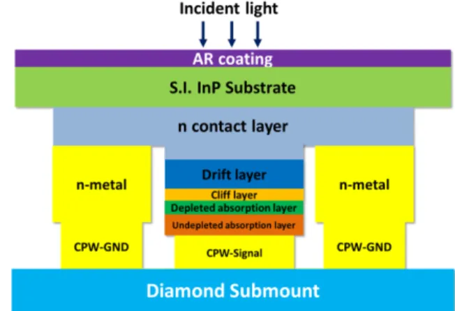
The PD epitaxial layer structure corresponds to a charge- compensated MUTC PD with both non-absorbing (InP) and absorbing (InGaAs) depletion regions[4]and was presented in Ref. [5]. The transparent electron drift layer (InP) is lightly n-type doped to compensate the electric field reduc- tion caused by the space charge in the
presence of high photocurrents[6]. A moderately doped clifflayer is integrated between the drift layer and the
Manuscript received December 26, 2014.
Manuscript revised March 31, 2015.
†The authors are with the Department of Electrical and Com- puter Engineering, University of Virginia, Charlottesville, VA 22904, USA.
a) E-mail: [email protected] DOI: 10.1587/transele.E98.C.764
absorber to enhance the electric field in the depleted por- tion of the absorption layer (Fig. 1 (b)). Back-illuminated double-mesa PDs were fabricated using standard dry etch- ing processes. Stacks of Ti/AuGe/Au and Ti/Pt/Au were used for n- and p-metal contacts, respectively. To facili- tate flip-chip bonding Au bonding bumps with a diameter of 6 µm and height of 2µm were plated on the p- and n- mesas to serve as electrical contacts and heat dissipation paths (Fig. 2).
A SiO2layer with a thickness of 250 nm was deposited on the back of the wafer as an anti-reflection coating. To improve thermal dissipation the 1 mm×1.3 mm MUTC PD dies were flip-chip bonded onto high-thermal conductivity submounts using an Au-Au thermo-compression bonding process[5]. Using AlN submounts we found that the max- imum dissipated power density of the photodiodes at the
Fig. 1 Band diagrams of (a) UTC and (b) MUTC photodiode.
Fig. 2 Simplified schematic cross-sectional view of a photodiode flip- chip-bonded on diamond submount.
Copyright c2015 The Institute of Electronics, Information and Communication Engineers
Fig. 3 Maximum output RF power vs. modulation frequency for single wideband photodiodes under continuous wave operation at 1.55µm wave- length.
point of failure was increased by 65% to 90% when com- pared to standard back-illuminated PDs without flip-chip bonding. We obtained even higher values when using di- amond submounts. Owing to the high thermal conductivity of the chemical-vapor-deposition diamond of>500 W/m/K, photodiodes with diameters of 50µm, 40 µm, 34µm, and 28µm reached RF output powers of 32.7 dBm at 10 GHz, 29.6 dBm at 15 GHz, 28 dBm at 20 GHz, respectively, and 26 dBm for a 28µm device at 25 GHz, without active cool- ing[7].
Compared with the 50µm-diameter MUTC PD on AlN submount reported in Ref. [8], the device bonded on dia- mond achieved 80% greater RF output power. The dissi- pated power in the device was as high as 2.5 W. The re- ponsivity was 0.75 A/W at 1.55µm and typical dark cur- rents were 500 nA. Recently, miniaturization of the PD ac- tive area and optimization of the microwave coplanar wave- guide (CPW) on chip enabled MUTC PDs with a 3-dB band- width of 65 GHz and an RF output power of 16 dBm[20].
In this design an air bridge connected the PD to a high- impedance (85 Ω) CPW transmission line, which served also as the bond pad in the flip-chip-bonding process. Since we designed the transmission line to provide slight inductive peaking, the bandwidth was significantly expanded beyond the conventional resistance-capacitance-limitation. Figure 3 summarizes our results together with data reported in the literature.
Using an optical heterodyne setup with a modulation depth close to 100% we measured a power conversion effi- ciency (PCE) of 42%, 38%, and 37% at 10 GHz, 20 GHz and 25 GHz, respectively, which compares favorably with previously reported results in Ref.[21]. An even higher PCE of 60% was obtained when using a Mach-Zehnder modula- tor biased away from its quadrature point[22].
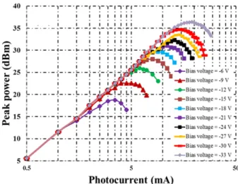
Recently, similar MUTC PDs were used to generate pulsed RF signals at 10 GHz. In the experiment we used a continuous wave (cw) fiber laser followed by two Mach- Zehnder modulators which generated the 10 GHz carrier and a 100-ns gate signal, respectively. Figure 4 shows the de- tected RF peak power versus average photocurrent for 20%
Fig. 4 Peak RF power at 10 GHz for bias voltages from−6 V to−33 V.
duty cycle and bias voltages in the range between −6 V and−33 V[23]. The peak power increases linearly as the photocurrent increases and then saturates due to the space- charge effect. The maximum RF peak power was 36.4 dBm (4.4 W) when the reverse bias voltage was 33 V and the aver- age photocurrent was 18 mA. Under these operating condi- tions PD failure occurred at a dissipated DC power of about 1 W, which is significantly less than the dissipated power at failure for cw illumination. While thermal failure be- comes less an issue we believe that photodiode operation under pulsed illumination was ultimately limited by junc- tion breakdown. Junction breakdown under dark conditions was observed at 36 V.
A fully packaged flip-chip bonded MUTC PD was demonstrated in Ref.[24]. The fiber-pigtailed hermetic PD module was equipped with a V-connector and included a Peltier element for active temperature control. We measured high RF output power levels reaching 25 dBm at 10 GHz and 17 dBm at 30 GHz under large-signal modulation. When il- luminated by short optical pulses an RF power of>21 dBm was measured at 10 GHz using selective RF filtering. A very low amplitude modulation (AM)-to-phase modulation (PM) conversion factor was also measured, making the PD module suitable for the use in photonic systems for ultralow phase noise high-power RF signal generation as described in Ref.[25].
A similar packaging concept was recently applied to a high-speed MUTC PD with 10-µm active diameter. The PD module demonstrated a 3-dB bandwidth of 50 GHz and an output power of 13.5 dBm at 50 GHz. It should be noted that the packaged photodiodes were operated safely at power levels well below the failure limitation. The RF loss in the photodiode module was estimated to be less than 2 dB up to 50 GHz.
3. MUTC PDs Integrated with Microwave Matching Circuits and Antennas
To improve output power and RF responsivity in a narrow
Fig. 5 Schematic (a) and micrograph (b) of PD on AlN substrate with open stub microwave matching circuits.
Fig. 6 Micrograph of flip-chip bonded PD with integrated coplanar an- tenna on AlN.
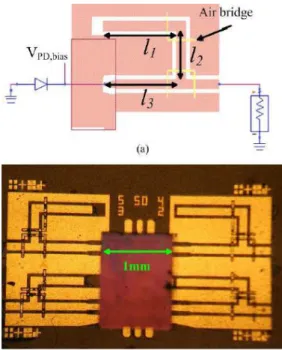
frequency band MUTC PDs were also integrated with mi- crowave matching circuits[26]. Figures 5 (a) and (b) show a layout of a PD with an open stub circuit and the fabricated circuit on AlN substrate after flip-chip bonding the MUTC photodiode chip, respectively[27].
By optimizing the lengths of the CPWs (l1, l2, and l3) the impedance of the PD was matched to the 50-Ω exter- nal load at an operating frequency of 20 GHz. Our devices achieved RF power levels as high as 23 dBm at 6 V bias volt- age and an average photocurrent of 140 mA. From a com- parison with a similar PD but without matching circuit we found a power enhancement of 6 dB.
Fig. 7 Received RF power at 60 GHz and RF compression versus aver- age photocurrent at 5 V after 6 cm free-space transmission[28].
In order to build a photonic mm-wave transmitter we also integrated the MUTC PD with a coplanar patch an- tenna. In our approach a 10-µm diameter PD was coupled to the antenna by flip-chip bonding (Fig. 6). Details about the antenna design can be found in Ref.[28]. Figure 7 shows the dependence of the received RF power on the average photocurrent of the antenna integrated PD at 60 GHz. The data was obtained for 6 cm free-space transmission using a receive-antenna with 15 dBi gain. The saturated receive power was−6.5 dBm at 5 V bias and the average photocur- rent was 45 mA. Using the definition in[29]we estimated the effective radiated power to be 20 dBm which indicates that −50 dBm can be received with an antenna of 25-dBi gain at a distance of 25 m from our photonic transmitter.
4. Summary
We have demonstrated that flip-chip bonded charge- compensated MUTC photodiodes can provide record-high output RF power levels up to 65 GHz. Integration with passive microwave circuits can further enhance performance and functionality in analog applications including photonic generation of low phase noise microwave signals and fiber optic antenna links.
References
[1] X. Li, N. Li, X. Zheng, S. Demiguel, J.C. Campbell, D.A.
Tulchinsky, and K.J. Williams, “High-saturation-current InP-In- GaAs photodiode with partially depleted absorber,” IEEE Photon.
Technol. Lett., vol.15, no.9, pp.1276–1278, 2003.
[2] F.J. Effenberger and A.M. Joshi, “Ultrafast, dual-depletion re- gion, InGaAs/InP pin detector,” J. Lightw. Technol., vol.14, no.8, pp.1859–1864, 1996.
[3] T. Ishibashi, N. Shimizu, S. Kodama, H. Ito, T. Nagatsuma, and T. Furuta, “Uni-traveling-carrier photodiodes,” Tech. Dig. Ultrafast Electronics and Optoelectronics, pp.83–87, 1997.
[4] D.-H. Jun, J.-H. Jang, I. Adesida, and J.-I. Song, “Improved efficien- cy-bandwidth product of modified uni-traveling carrier photodiode structures using an undoped photo-absorption layer,” Japan. J. Appl.
Phys., vol.45, no.4B, pp.3475–3478, 2006.
[5] Z. Li, Y. Fu, M. Piels, H. Pan, A. Beling, J.E. Bowers, and J.C.
Campbell, “High-power high-linearity flip-chip bonded modified uni-traveling carrier photodiode,” Optics Express, vol.19, no.26, 2011.
[6] N. Li, H. Chen, S. Demiguel, X. Li, J.C. Campbell, T.D. Isshiki, G.S. Kinsey, and R. Sudharsansan, “High-Power Charge-Compen- sated Unitraveling-Carrier Balanced Photodetector,” IEEE Photon.
Technol. Lett., vol.16, no.10, pp.2329–2331, 2004.
[7] X. Xie, Q. Zhou, K. Li, A. Beling, and J.C. Campbell, “1.8 Watt RF Power and 60% Power Conversion Efficiency Based on Photodiode Flip-chip-bonded on Diamond,” in CLEO: 2014 Postdeadline Paper Digest, OSA Technical Digest (online) (Optical Society of America, 2014), paper JTh5B.9.
[8] Q. Zhou, A.S. Cross, F. Yang, A. Beling, and J.C. Campbell, “Devel- opment of narrowband modified uni-travelling-carrier photodiodes with high power efficiency,” in Avionics, Fiber-Optics and Photon- ics Conference (AVFOP) 2013 (IEEE, 2013), pp.65–66.
[9] X. Li, S. Demiguel, N. Li, J.C. Campbell, D.L. Tulchinsky, and K.J.
Williams, “Backside illuminated high saturation current partially de- pleted absorber photodetectors,” Electron. Lett., vol.39, no.20, Oct.
2003.
[10] Z. Li, Y. Fu, H. Pan, A. Beling, and J.C. Campbell, “Photodiode with 0.75 W RF Output Power at 15 GHz,” in Proc. 37th Europ.
Conf. Optical Commun. (ECOC 2011), Geneva, Switzerland, Sept.
2011.
[11] N. Duan, N. Li, S. Demiguel, and J.C. Campbell, “An InGaAs/InP Photodiode with 600 mW RF Output Power,” in 19thAnnu. Meeting IEEE Lasers Electro-Optics Soc.(LEOS 2006), Oct. 2002, pp.52–53, paper WD2.3.
[12] K. Sakai, E. Ishimura, M. Nakaji, S. Itakura, Y. Hirano, and T. Aoyagi, “High-Current Back-Illuminated Partially Depleted-Ab- sorber p-i-n Photodiode With Depleted Nonabsorbing Region,”
IEEE Trans. Microwave Theory Tech., vol.58, no.11, pp.3154–3160, 2010.
[13] N. Shimizu, Y. Miyamoto, A. Hirano, K. Sato, and I. Ishibashi, “RF Saturation mechanism of In/InGaAs uni-travelling-carrier photodi- ode,” Electron. Lett., vol.36, no.8, pp.750–751, April 2000.
[14] D.A. Tulchinsky, J.B. Boos, D. Park, P.G. Goetz, W.S. Rabinovich, and K.J. Williams, “High-Current Photodetectors as Efficient, Lin- ear, and High-Power RF Output Stages,” J. Lightw. Technol., vol.26, no.4, pp.408–416, 2008.
[15] X. Wang, N. Duan, H. Chen, and J.C. Campbell, “InGaAs–InP pho- todiodes with high responsivity and high saturation power,” IEEE Photon. Technol. Lett., vol.19, no.16, pp.1272–1274, 2007.
[16] M. Chtioui, A. Enard, D. Carpentier, S. Bernard, B. Rousseau, F.
Lelarge, F. Pommereau, and M. Achouche, “High-Power high-lin- earity uni-traveling-carrier photodiodes for analog photonic links,”
IEEE Photon. Technol. Lett., vol.20, no.3, pp.202–204, 2008.
[17] Z. Li, H. Pan, H. Chen, A. Beling, and J.C. Campbell, “High Satura- tion Current Modified Uni-Traveling-Carrier Photodiode with cliff layer,” IEEE J. Quantum Electronics, vol.46, no.5, pp.626–632, 2010.
[18] N. Li, X. Li, S. Demiguel, X. Zheng, J.C. Campbell, D.A.
Tulchinsky, K.J. Williams, T.D. Isshiki, G.S. Kinsey, and R. Sudharsansan, “High-Saturation-Current Charge-Compensated InGaAs InP Uni- Traveling-Carrier Photodiode,” IEEE Photon.
Technol. Lett., vol.16, no.3, pp.864–866, 2004.
[19] M. Chtioui, F. Lelarge, A. Enard, F. Pommereau, D, Carpentier, A.
Marceaux, F. Van-Dijk, and M. Achouche, “High Responsivity and High Power UTC and MUTC GaInAs-InP Photodiodes,” IEEE Pho- ton. Technol. Lett., vol.24, no.4, pp.318–320, 2012.
[20] Q. Zhou, A.S. Cross, A. Beling, Y. Fu, Z. Lu, and J.C. Campbell,
“High-power V-band InGaAs/InP Photodiodes,” IEEE Photon.
Technol. Lett., vol.25, no.10, pp.907–909, 2013.
[21] U. Gliese, K. Colladay, A.S. Hastings, D.A. Tulchinsky, V.J. Urick, and K.J. Williams, “53.5% Photodiode RF Power Conversion Ef- ficiency,” in Optical Fiber Communication Conference (OFC2010)
paper PDPA7, 2010.
[22] X. Xie, Q. Zhou, K. Li, A. Beling, J.C. Campbell, “1.8 Watt RF Power and 60% Power Conversion Efficiency Based on Photodiode Flip-chip-bonded on Diamond,” CLEO 2014, San Jose, CA, 8-13 June, 2014, Postdeadline paper 2 (JTh5B).
[23] X. Xie, Q. Zhou, K. Li, A. Beling, and J.C. Campbell, “Photonic Generation of High-Power Pulsed Microwave Signals with Peak Powers up to 7.2 Watt,” Optical Fiber Communication Conference (OFC 2015), OSA Technical Digest (online) (Optical Society of America, 2015), paper Tu3F.2, 2015.
[24] E. Rouvalis, F.N. Baynes, X. Xie, K. Li, Q. Zhou, F. Quinlan, T.M.
Fortier, S.A. Diddams, A.G. Steffan, A. Beling, and J.C. Campbell,
“High-Power and High-Linearity Photodetector Modules for Mi- crowave Photonic Applications,” Journal of Lightwave Technology, vol.32, no.20, pp.3810–3816, 2014.
[25] T.M. Fortier, F. Quinlan, A. Hati, C. Nelson, J.A. Taylor, Y. Fu, J.C.
Campbell, and S.A. Diddams, “Photonic microwave generation with high-power photodiodes,” Opt. Lett. vol.38, no.10, pp.1712–1714, 2013.
[26] H. Ito, Y. Hirota, A. Hirata, T. Nagatsuma, and T. Ishibashi,
“11 dBm photonic millimetre-wave generation at 100 GHz using uni-travelling-carrier photodiodes,” Electron. Lett., vol.37, no.20, pp.1225–1226, Sept. 2001.
[27] K. Li., X. Xie, Q. Zhou, A. Beling, and J.C. Campbell, “High Power 20-GHz Photodiodes With Resonant Microwave Circuits,” IEEE Photon. Technol. Lett., vol.26, no.13, pp.1303–1306, 2014.
[28] K. Li, X. Xie, Q. Li, Y. Shen, M.E. Woodsen, Z. Yang, A. Beling, J.C. Campbell, “High-Power Photodiode Integrated with Coplanar Patch Antenna for 60 GHz Applications,” accepted for publication in Photon. Technol. Lett., vol.27, no.6, pp.650–653, 2015.
[29] K. Takahata, Y. Muramoto, S. Fukushima, T. Furuta, and H.
Ito, “Monolithically integrated millimeter-wave photonic emitter for 60-GHz fiber-radio application,” presented at the Microwave Photonics Conference (MWP 2000), Oxford, UK, paper WE3.4, pp.229–232, 2000.
Andreas Beling received the Dipl.-Phys.
degree (M.S.) in physics from the University of Bonn, Germany, in 2000 and the Dr.-Ing. degree (Ph.D.) in electrical engineering from Techni- cal University Berlin, Germany, in 2006. He was a staffscientist in the photonics division at the Heinrich-Hertz-Institute in Berlin in 2001–
2006, a Research Associate in the Department of Electrical and Computer Engineering at the Uni- versity of Virginia in 2006–2008, and has two years of industry experience as a project man- ager working on optical communication devices. He returned to Univer- sity of Virginia and became Assistant Professor in the Department of Elec- trical and Computer Engineering in 2013. His research interests include high-speed optoelectronic devices, photonic integrated circuits, microwave photonics, and optical communications. Andreas Beling has authored or co-authored more than 110 technical papers, two book chapters, and four patents. Dr. Beling is a Senior Member IEEE and became an Associate Editor of the IEEE/OSA Journal of Lightwave Technology in 2014.
Joe C. Campbell received the B.S. De- gree in Physics for the University of Texas at Austin in 1969, and the M.S. and Ph.D. de- grees in Physics from the University of Illinois at Urbana-Champaign in 1971 and 1973, respec- tively. From 1974 to 1976 he was employed by Texas Instruments where he worked on in- tegrated optics. In 1976 he joined the staff of AT&T Bell Laboratories in Holmdel, New Jersey. In the Crawford Hill Laboratory he worked on a variety of optoelectronic devices including semiconductor lasers, optical modulators, waveguide switches, photonic integrated circuits, and photodetectors with emphasis on high- speed avalanche photodiodes for high-bit-rate lightwave systems. In Jan- uary of 1989 he joined the faculty of the University of Texas at Austin as Professor of Electrical and Computer Engineering and Cockrell Family Regents Chair in Engineering. In January of 2006, Professor Campbell be- came a member of the faculty at the University of Virginia in Charlottesville as the Lucian Carr, III Chair of Electrical Engineering and Applied Science.
Professor Campbell’s research has focused on the optoelectronic compo- nents that are used to generate, modulate, and detect the optical signals. At present he is actively involved in single-photon-counting avalanche photo- diodes, Si-based optoelectronics, high-speed, low-noise avalanche photodi- odes, ultraviolet photodetectors, and quantum-dot IR imaging. To date he has coauthored ten book chapters, 400 articles for refereed technical jour- nals, and more than 400 conference presentations. He is a member of the National Academy of Engineering.
Kejia Li was born in Tianjin, China. She re- ceived the M.S. degree in Electrical Engineering from Peking University in 2008, and the Ph.D.
degree in Electrical Engineering from Univer- sity of Virginia in 2012. She is currently a re- search scientist in Joe C. Campbell Group, Uni- versity of Virginia, Charlottesville. Her current research interests include high-power photode- tectors and microwave photonics.
Qinglong Li was born in Tianjin, China in 1985. He received his bachelor degree at Nankai University in Tianjin in 2008. Later, he worked in Semiconductor manufacturing indus- try in China for 1.5 years. After which, he con- tinued his graduate study and received his Mas- ter of Science degree at Rochester Institute of Technology, NY, US in 2013. He is currently pursuing his Ph.D. degree in JCC group at ECE department at University of Virginia in Char- lottesville, VA, US with his research interests focusing on high power and high speed photo-detector for optical com- munication application.
Ye Wang has been a Ph.D. student in the ECE department at U.Va. since 2014. He re- ceived his B.E. in Optoelelctronic Information Engineering from Huazhong University of Sci- ence and Technology (HUST), 2014. Ye’s re- search interests focus on design, fabrication and characterization of high power photodiodes and MWIR Multi-Quantum Well (MQW) detectors.
Madison Woodson received her B.S. de- gree in biomedical engineering with a minor in electrical engineering from the University of Virginia, Charlottesville, in 2013, and is cur- rently pursuing an electrical engineering Ph.D.
within the Electrical Engineeirng Department of the University of Virginia. Her current research interest focus on using Monte Carlo simulations to model semiconductor device physics for pho- todetector applications.
Xiaojun Xie received his B.S. in optical information science and technology from Uni- versity of Electronic Science and Technology of China (UESTC), China, in 2010, and M.S.
in electromagnetic field and microwave tech- nology from Beijing University of Posts and Telecommunications (BUPT), China, in 2013.
He is currently pursing Ph.D. in electrical engi- neering at University of Virginia, USA. His re- search interests lie in the design, fabrication and characterization of high power and high linear- ity photodiodes as well as the high-performance photodiodes application on analog photonics link and pulsed RF signal generation. He also focuses on InP photodiode integration on silicon photonic-electronic platform.
Zhanyu Yang was born in Anhui Province, China, in 1989, and received the B.S. degree in physics from Beijing Capital Normal Univer- sity (CNU) in 2010. In 2013, he received the M.S. degree from State Key Laboratory of Infor- mation Photonics and Optical Communications, Beijing University of Posts and Telecommuni- cations (BUPT), China. He is currently working toward his Ph.D degree in Electrical and Com- puter Engineering at University of Virginia. His research interest focus on high power photodi- odes and their applications in analog links.