Japan Advanced Institute of Science and Technology Title
シリコン(001) 2×1表面上に配向した個々の4,4"‑ジア ミノpターフェニル分子の走査型トンネル顕微鏡による ナノスケール解析
Author(s) Amer Mahmoud, Amer Hassan Citation
Issue Date 2014‑09
Type Thesis or Dissertation Text version ETD
URL http://hdl.handle.net/10119/12299 Rights
Description Supervisor:富取 正彦, マテリアルサイエンス研究科
, 博士
Nanoscale analysis of alignment of individual 4,4’’-diamino-p-terphenyl
molecules deposited on Si(001)-2x1 observed by scanning tunneling microscopy
AMER MAHMOUD AMER HASSAN
Japan Advanced Institute of Science and Technology
Doctoral Dissertation
Nanoscale analysis of alignment of individual 4,4’’-diamino-p-terphenyl
molecules deposited on Si(001)-2x1 observed by scanning tunneling microscopy
AMER MAHMOUD AMER HASSAN
Supervisor: Professor Masahiko Tomitori
School of Materials Science
Japan Advanced Institute of Science and Technology
September 2014
observed by scanning tunneling microscopy.
Keywords: molecule; diamino-p-terphenyl; silicon; butterfly bonding; scanning tunneling microscopy
Abstract
Organic molecular electronics has attracted much interest to fabricate innovative products with high performance at low cost, and furthermore to open novel architecture for future device processes. To improve their characteristic performance, the conformational alignments and bonding states of individual organic molecules in the devices are crucial. Selection and preparation of molecule-binding substrates also dominate the performance, and a wide-ranging survey for the molecule-substrate combination is indispensable.
In this study scanning tunneling microscopy (STM) observation was conducted for 4,4”-diamino-p-terphenyl (DAT) molecules deposited on a clean reconstructed Si(001)-(2×1) surface at room temperature (RT). The Si surface can be a good candidate for a substrate to examine molecular adsorption. In this study, the linear but twisted π- conjugated framework of DAT, were mostly revealed to lie down laterally on the surface, which has a linear framework consisting of a central benzene ring and two phenyl rings (terphenyl) terminated with two amino groups at both ends.
The DAT was evaporated by heating a crucible containing the DAT at a temperature ranged from 418 to 433 K, which was below the DAT melting temperature of ~510 K. The depositing amount of the DAT molecules on the Si(001) surface was controlled by changing the opening time of a mechanical shutter over the crucible, ranging from a few seconds to a few minutes.
The majority of DATs were tilted laterally at about 17° with respect to the direction of a Si dimer row on the surface, though a variety of DAT configuration with different angles was found by STM. The histograms of the tilted angles at low coverages (0.04 molecule/nm2) showed that the most frequent angle was 17°. The DATs tilted at 17°
looked hollow at the center and their apparent height was lower than that of other configurations of DAT in STM images. This indicates that the DAT tends to take a double arched shape at the tilted angle of 17° in a stable conformation with butterfly-like bonding through the central ring to a Si dimer as well as the two amino groups bonded to respective Si atoms on the dimer row.
The DAT molecules adsorbed on the Si(001) surfaces at low coverages were annealed at 523 K for 1 min, and the surfaces were examined by STM. The number at 17° increased from 50% to about 80%, while the number of molecules at a tilted angle of 8° and 0° decreased less than 15%, and the number at other angles diminished within our total counting of about 250 protrusions. It is probable that the protrusion at 17° was the most stable irrespective of annealing, corresponding to a chemical configuration of DAT absorbed on the Si(001)-(2×1) surface. The deposition amount of DAT was increased to 0.24 molecule/nm2 and annealed at 523 K for 1 min. STM images showed that the DAT at high coverages (0.24 molecules/nm2 or more) turned out to be linearly ordered structure running to the direction of about 22° with respect to the Si dimer row.
The results obtained in this study showed that the amino groups of molecules interacted with Si surfaces at RT, and phenyl rings also interacted with Si dimers between their π state electron orbitals. The well-defined Si surface exhibited to hold the proper characteristics to reveal the interaction with the molecules. The results also showed the potential for the DAT and Si system leading to a fundamental layer to grow the overlayer with their well-defined configuration for future molecular electronics.
Professor Masahiko Tomitori
Japan Advanced Institute of Science and Technology
Referees:
Professor Goro Mizutani
Japan Advanced Institute of Science and Technology Professor Hideyuki Murata
Japan Advanced Institute of Science and Technology Professor Yoshifumi Oshima
Japan Advanced Institute of Science and Technology Professor Hidemi Shigekawa
Institute of Applied Physics - University of Tsukuba
Tomitori for giving me this great chance to study at JAIST and to be a member of his laboratory group, during my PhD study, in addition to his supervision for my PhD, I feel that he is a very kind friend for me, usually giving me great advices, activating my research thinking, developing my scientific skills, teaching me how to follow the logic steps to support my scientific research, taking care about my life conditions and kindly accepting my impressions in scientific and life situations.
I would like to express my deep thanks to the internal committee members Professor Goro Mizutani, Professor Hideyuki Murata and Professor Yoshifumi Oshima, School of Materials Science at JAIST and my special thanks to Professor Hidemi Shigekawa from Institute of Applied Physics at University of Tsukuba as an external committee. I really appreciate their working time as referees of my thesis.
My great thanks to Professor Hideyuki Murata and his laboratory members for welcoming and supporting me to do my sample purification experiment in his laboratory.
My special thanks to Professor Hiroshi Mizuta and his laboratory members for welcoming and supporting me to complete my minor research, many thanks to Dr.
Manoharan Muruganathan for his kind help.
I would like to express my deep thanks to my laboratory members, Assist. Prof.
Akira Sasahara, Mrs. Miho Hashimoto, Dr. Takashi Nishimura, Mr. Tomoko Miyagi, Mrs. Le Tran Uyen Tu, Mr. Makoto Nogami, Miss. Tatsumi Hitomi, and Mr.
Tetsuya Yoshi for their help and their kind feelings.
Many thanks to Professor Masato Oda from Department of Materials Sciences and Chemistry, Wakayama University for valuable discussion.
Many thanks to the Japanese Society for the Promotion of Science, Grants-in-Aid for Scientific Research for supporting this work.
Finally, my deepest thanks are to my parents and all my family in Egypt, my special thanks to my wife and my sons for joining me in this stay at JAIST and supporting me by pure love and kind feelings.
Amer Mahmoud Amer Hassan Tomitori’s lab., JAIST, Ishikawa Japan.
Chapter 1 Introduction
1.1 Background of organic molecules on silicon substrates 1 1.2 Nano scale analysis of molecules by scanning probe microscopy 6 1.3 π-conjugated organic molecules: 4,4”-diamino-p-terphenyl
(DAT)
8
Chapter 2 Experimental Principles
2.1 Scanning tunneling microscopy (STM) 15
2.2 Fabrication of molecular layers on silicon substrates in ultrahigh vacuum
19
Chapter 3 Experimental Methods
3.1 Substrate preparation: clean Si(001)-2×1 surface 22 3.2 DAT deposition on Si(001) at low coverages 28
3.3 Model calculation of DAT on Si(001) 31
3.4 Preparation and evaluation of STM tungsten tips 35 Chapter 4 Results and Discussion
4.1 STM observation of Si(001) 52
4.2 DAT deposited Si(001) surfaces at low coverages 62
4.3 Alignments of DAT on Si(001) 82
4.4 Fabrication of one monolayer of DAT on Si(001) 85
4.5 Stable structures of DAT on Si(001) 89
Chapter 5 Conclusions 102
Chapter 6 Prospective Summary 103
Appendix 105
1
1-Introduction:
1.1 Background of organic molecules on silicon substrates
To date a great number of applications using organic films have rapidly been examined, because a variety of fascinating chemical and physical properties of the films have been revealed, depending on not only their bulk structures in the films but also their specific chemical configurations on film substrates. The organic films have increasingly taken important roles in materials engineering.
Their wide range of properties and applications are not inferior to other major classes of materials, such as steel and silicon. The competition in chemical, electronic and fine mechanical industries to establish the processes for device fabrication of organic films and to take the initiative in the market is globally keen. Since the basic and technical knowledge on organic films holds the key to improve their performance and to win the competition, basic researches to understand their material properties are indispensable.
Among their promising applications organic electronic devices have attracted much interest to fabricate innovative products with high performance at low cost utilizing molecular specific electronic and mechanical properties.
For example, organic electroluminescence has considerable potential for applications to ubiquitous display devices because of the high light-emitting efficiency and a variety of tunable colors [1] using multilayer structures,[2]
doped emitting layers,[3] novel transport and luminescent materials[4] including flexible polymers,[5,6] and efficient injection contacts.[7]
It has been widely recognized that the twentieth century was the time of silicon (Si), initiated by the invention of a solid-state transistor with semiconducting materials; at the present a tremendous amount of silicon electronic devices have prevailed all over the world. During the development of Si devices including the lithographic techniques to miniaturize the devices, the science and technology concerning Si have extremely progressed; for example,
2
the high-quality of the single crystal, ultimate control of impurities, and polishing and flattening of Si single crystal surfaces. To extend and explore the new device technology with organic films, the combination of the organic films with Si is one of the most promising and reasonable approaches. For example, Si substrates for deposition of organic molecules are of great interest to realize novel functionalized electronic devices. To improve the electronic properties of the devices, it is crucial to control the interfaces between Si substrates and organic molecules.
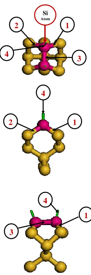
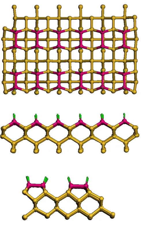
Here as a basic surface science, the Si surface structure is referred. As a starting point, the (001) surface of silicon (Figure 1.1) acts as the representative of substrates from a technological viewpoint for nano electronic devices using the wide-range Si technology. Cleaving the silicon crystal along the (001) plane, each silicon surface atom has four bonds: two bonds (Figure 1.2; bond number 1 and 2 are shown therein) to the bulk and the remnant two bonds on the surface (bond number 3 and 4). Two silicon atoms at the surface share two electrons with the nearest silicon atom forming a dimer (pink color in Figure 1.1). Every pair of silicon atoms forms one dimer and leaves two bonds free as dangling bonds, which are ready to be a good stand for depositing molecules.
To reveal the adsorption configuration and to control the alignments of organic molecules on the well-defined Si surface, a large number of reports have been published; for example, amino-terminated organic monolayers on hydrogen-terminated silicon surfaces, Alexander et al. [8] developed two new routes for the preparation of amino-functionalized monolayers on H-terminated Si surfaces. Both routes are based on a two-step procedure in which a mixed monolayer was prepared of a protected ω-amino-1-alkene and a nonfunctional 1-alkene was prepared. Subsequent removal of the protective groups then generates the covalently attached NH2-terminated monolayer without damaging the underlying Si surface or the monolayer composition. Another example, amino-terminated organic monolayers covalently modified silicon surface, Tami
3
Figure1.1 Top and side views of a Si(001)-(2×1) surface.
Si dimer rows are illustrated in pink color.
Si dimer line
4
et al. [9] established a method for minimizing nonspecific binding that can significantly enhance the ability to integrate biological molecules, especially proteins, with microelectronic materials.
In fabrication of stable chemical bonding of molecules to Si substrates, amino group containing molecules play important roles, because a N atom in the amino group with a lone pair of electrons can interact with Si substrates and act as an electron donor, leading to prominent chemical and electrical properties.
Electronic and vibrational spectroscopies showed that surface layers deposited with the molecules of NH3 on Si(100)-(2×1) comprised coadsorbed NH2 and H at room temperature (RT).[10-13] An early study was interpreted in terms of subsurface atomic N and adsorbed H [14]. At present, however, it is accepted that NH2 and H species are adsorbed at the opposite ends of Si dimers on the Si(100)-(2×1) clean surface, resulting in change in the Si dimer asymmetry relative to that of the clean surface.[15] To clarify the structures of molecules adsorbed on the substrates, not only STM observation but also guidelines to optimize models for molecule-substrate systems are indispensible.[16-19]
In this study, 4,4”-diamino-p-terphenyl (DAT) is deposited on the Si(001)-(2×1) surface at low coverages at room temperature (RT) by vapor deposition, and observed by STM to reveal the DAT configurations and find the most stable one on it. Furthermore, the surface is annealed to draw the evidence to align DATs on the surface to pursue their stable configuration with changing depositing amount. DAT has been used for a monomer of conjugated polymer, polyazomethine, which was employed for electroluminescence (EL) devices prepared by vapour deposition polymerization. It is important to examine the annealing effects. Fabrication of one monolayer and control of the interface between DAT and substrate possibly improve the performance of electronic properties, so that alignment and fabrication of one monolayer of DAT on Si surface is one of main concerns of this study.
5
1.2 Nanoscale analysis of molecules by scanning probe microscopy
1 2
4 3
Si
Atom
1 2
4
1 3
4
Figure 1.2 Model of Si(001) surface. Si bonds to the bulk denoted by 1 and 2.
Forming a dimer with a nearest surface Si atom using a bond denoted by 3.
Dangling bond denoted by 4.
6
1.2 Nano scale analysis of molecules by scanning probe microscopy The word of “nano” means the 10-9 power, i.e., one billionth. Atomic diameters and molecular sizes are usually measured by the unit of a nanometer. For comparison, a human hair is about 100,000 nanometers (nm) in diameter. Nano science is the study of atoms, molecules, and objects whose size is on the nanometer scale (1-100 nm). Physical and chemical properties of nanoscale materials have attracted much interest due to their infinite potentials for functional device application. They are, however, much different than those of bulk, where quantum mechanical properties not seen on a macroscopic scale are dominant in the nanoscale world. Rather than working with bulk materials, one works with individual atoms, small clusters (consisting of a small number of atoms) or molecules to realize exotic functional materials using their properties.
By learning about properties of individual clusters or molecules, we can put them together in very well-defined ways to produce new materials with new and amazing functionalities with increasing efficiency and reliability. The investigation techniques from an atomic resolution point of view are indispensable and essential to understand the nanoscale structural and electronic properties of various materials. High-resolution microscopes historically played an important role for their characterization.
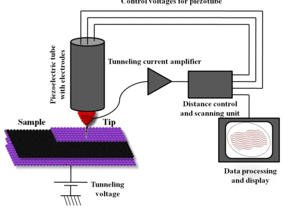
One of major tools for fabrication and characterization in nanoscience and nanotechnology is scanning probe microscopy (SPM). In particular, we can investigate the fundamental relationships between nano structures and nano physical properties using it. The term of SPM typically covers STM, atomic force microscopy (AFM), near-field scanning optical microscopy (NSOM, or SNOM) and related techniques. Today several atom-resolved microscopic techniques are available. One of them is the STM that uses an atomically sharpened metallic needle (tip). The operation principle is illustrated in Figure 3.
7
Figure 1.3 Principle and schematic of STM.
8
In STM the tip is brought close to a sample, and maintain a constant separation between the tip and a sample using a feedback circuit control which measures the electric tunneling current between them. The STM can be applied not only for characterization but also for manipulation of a variety of nanostructures, including solid-state matter, organic materials and biomaterials, in various environments as vacuum, ambient conditions, and even liquids.
The SPM including the STM has now been regarded as one of the major driving forces for rapid development of nanoscience and nanotechnology, and the tool of choice in many areas of research. In principle it is interesting that the SPM techniques operate on the basis of the quantum mechanical features of electrons and atomic interactions.
1.3 π-conjugated organic molecules:4,4’’-diamino-p-terphenyl (DAT) Although it is needed to characterize and improve organic molecular thin films for applications in opto- and nano- electronic devices, in particular, electroluminescence devices, the complicated nature of the structures of these organic molecular films raises some of fundamental questions about their vibrational excitations, electronic and excitonic properties, correlation effects random disorder of the structure and thermal fluctuations. While the wide research about the basic phenomena to improve the performance of devices, such as charge carrier injection into and transport through thin films has been still not perfectly understood even for inorganic solids. The complicated of relaxation and polarization phenomena control the mechanism of the energy levels of charge carriers. The covalently bonded inorganic semiconductors have strong resonance interactions between neighboring atoms, which affect the stability of charge carriers and delocalized them. The energy levels and the transport of charge carriers are described within the single-electron band approximation. Polarization energy are small, carrier screening is efficient and
9
binding energies are few meV[20]. The minimum energy of formation of a separated free electron and hole, i.e., the transport gap, is therefore very close to the onset of optical absorption, i.e., the optical gap. This gap is used for accurate modeling of charge carrier injection at the semiconductor interfaces.
On the other hand, localization and polarization phenomena dominate the physics of charged excitation and transport in organic molecular solids.[22, 23]
Organic solids have low dielectric constants, small intermolecular overlap, charges localized on individual molecules and large polarizabilities involving charges and induced dipoles. The optical gap corresponds to the formation of a Frenkel exciton, with the electron and hole on the same molecule, rather than to a band-to-band transition.[21, 24]
Applications of polymer light-emitting diodes (PLEDs) increased gradually after the discovery of electroluminescence devices in conjugated polymers by Burroughes et al.[25] There are many barbed points should be fixed for manufacturing for practical application. The most important point is the lifetime of PLEDs by fabrication of light-emitting polymers such as poly(p- phenylenevinylene) (PPV) by wet process. This process is simple and low-cost process, but it has some disadvantages. For example, the adsorbed impurities such as solvents and atmospheric water cannot be completely removed from polymer films which are the reasons for degradation of PLEDs.[26]
To solve this problem, vapor deposition polymerization (VDP) help us to fabricate conjugated polymer film on a substrate by direct deposition of monomers without solvents, which decrease the impurities in polymer films. In addition, VDP process is easier to control the fabrication process of multi-layer structure, increasing the efficiency of multi-layer structure for PLEDs. Another advantage of the vapor deposition process has a good control of film uniformity and thickness over solution-based techniques. In addition, if the polymer becomes insoluble after film formation, the polymer layer can be used for patterned by photolithography technique. [27]
10
Another example, the thin films of PPV and polyoxadiazole (POD) have been fabricated with the VDP method.[28-31] These materials usually fabricated by a two-step reaction process, the first step, fabricating polymer by polymerization of monomer, and then converts to the final products by annealing above 200 °C and close to 300 °C. The final product of PPV and POD are insoluble for any organic solvents. Applications of PPV[29] and POD[30,31] thin films prepared by VDP for active layer of PLEDs have been reported.
On the other side, polyazomethine (PAM) thin films can be prepared by only one-step reaction process, with substrate temperature below 200 °C, the low-temperature process allows us to use plastic substrates. Application of PAM films for organic light-emitting diodes (OLEDs) have been employed previously [32-34]. However, these reports used only PAM films as carrier transporting layers of OLEDs. The electroluminescence from PAM prepared by VDP process has never been reported.
In this study, we report successful fabrication of DAT molecule layers of a monomer of PAM on silicon substrate. Nishimura et al.[35] deposited DAT molecules on a Si(111)-(7×7) surface at RT and examined using X-ray photoelectron spectroscopy (XPS) and STM. Figure 1.4 shows the chemical structure of DAT consisting of a linear but twisted three-benzene chain (π- conjugated), i.e., terphenyl, and two amino groups at the two ends of the chain.
DAT is a monomer used to synthesize a conjugated polymer by vapor deposition polymerization through the amino groups[36]. At low coverages of DAT, Nishimura et al. found that the DAT was chemically bonded to the Si surface through one amino group at one end of the DAT even at RT, and the other amino group was not bonded to the surface, resulting in the main framework of DAT standing at a slant onto the Si(111) surface. Meanwhile, to form ordered molecular multi-layers over long distances through π-π stacking interaction, the molecules lying-down parallel to their substrate is preferable,
11
which are profitable to light-emitting and photovoltaic molecular devices[37].
Their lying-down configuration can be triggered at the interface between the first layer molecules and the substrate. Since the reconstructed Si(001)-(2×1) surface has a number of Si dangling bonds larger than that of the Si(111)-(7×7) surface per area, the molecules with orbitals deposited on the Si(001)-(2×1) surface can take a diversity of alignments on it, possibly leading to their lying down configuration. In this study, we examine the adsorption of DAT on the Si(001)-(2×1) surface at RT, and analyze the conformational change by annealing to pursue the stable alignments and to fabricate ordered structures suitable for molecular devices.
Figure 1.4 (a) Chemical structure of DAT. (b) optimized structure of DAT using Material Studio[38].
(a)
(b)
12
References
1) J. Kido, M. Kimura, and K. Nagai, Science 267 (1995) 1332.
2) C. W. Tang and S. A. Van Slyke, Appl. Phys. Lett. 51 (1987) 913.
3) C. W. Tang, S. A. Van Slyke, and C. H. Chen, J. Appl. Phys. 65 (1989) 3610.
4) C. Hosokawa, H. Higashi, H. Nakarmura, and T. Kusumoto, Appl. Phys.
Lett. 67 (1995) 3853.
5) D. Braun, E. G. J. Staring, R. C. J. E. Demandt, G. L. J. Rikken, Y. A. R. R.
Kessener, and A. H. J. Venhuizen, Synth. Met. 66 (1994) 75.
6) D. R. Baigent, N. C. Greenham, J. Gruner, R. N. Marks, R. H. Friend, S. C.
Moratti, and A. B. Holmes, Synth. Met. 67 (1994) 3 .
7) Y.Yang, E. Westerweele, C. Zhang, P. Smith, and A. J. Heeger, J. Appl.
Phys. 77 (1995) 694.
8) A. B. Sieval, R. Linke, G. Heij, G. Meijer, H. Zuilhof, and E. J. R. Sudho, Langmuir 17 (2001) 7554.
9) T. L. Lasseter, B. H. Clare, N. L. Abbott, and R. J. Hamers, J. Am. Chem.
Soc. 126 (2004) 10220.
10) F. Bozso and Ph. Avouris, Phys. Rev. Lett. 57(1986)1185.
11) E. K. Hill et al., Phys. Rev. B 35 (1987) 5913.
12) F. Bozso and Ph. Avouris, Phys. Rev. B 38 (1988) 3937.
13) M. Fujisawa, Y.Taguchi, Y. Kuwahara, M. Onchi, and M. Nishijima, Phys.
Rev. B 39 (1989) 12918.
14) R. J. Hammers, Ph. Avouris, and F. Bozso, Phys. Rev.Lett. 59 (1987) 2071.
15) N. Franco, J. Avila, M. E. Davila, M. C. Asensio, D. P. Woodruff, O. Schaff, V. Fernandez, K.-M. Schindler, V. Fritzsche, and A. M. Bradshaw, Phys.
Rev. Lett. 79 (1997) 673.Ph
16) P. G. Piva, G. A. DiLabio, J. L. Pitters, J. Zikovsky, W. A. Hofer, and R. A.
Wolkow, Nature 435 (2005) 658.
13
17) W. Kim, H. l Kim, G. Lee, Y. K. Hong, K. Lee, C. Hwang, D. H. Kim, and J. Y. Koo, Phys. Rev. B 64 (2001) 193313.
18) B.J. Eves, Q.Y. Sun, G. P. Lopinski, and H. Zuilhof, J. Am. Chem. Soc.126 (2004) 14318.
19) P. Kruse, E. R. Johnson, G. A. DiLabio, and R. A. Wolkow, Jr. Nano Lett. 2 (2002) 807.
20) M. J. Bozack. P. A. Taylor, W. J. Choyke, and J. T. Yates, Jr., Surf. Sci. 177 (1986) L933.
21) I. G. Hill, A. Kahn, Z. G. Soos, R. A. Pascal, Jr., Chem. Phys. Lett. 327 (2000) 181.
22) M. C. E. Pope, Electronic Process in Organic Crystals, Clarendon Press, Oxford University Press, Oxford (1982).
23) E. A. Silinsh, V. Capek, Organic Molecular Crystals, AIP Press, New York (1994).
24) N. S. Sariciftci (Ed)., Primary Photoexcitations in ConjugatedPolymers:
Molecular Exciton versus Semiconductor Band Model, WorldScientific (1997).
25) H. Burroughes, D. D. C. Bradley, A. R. Brown, R. N. Marks, K. Macay, R.
H. Friend, P. L. Burns and A. B. Holmes, Nature 347 (1990) 539.
26) T. Ikeda, H. Murata, Y. Kinoshita, J. Shike, Y. Ikeda and M. Kitano, Chem.
Phys. Lett. 426 (2006) 111.
27) K. M. Vaeth and K. F. Jensen, Adv. Mater. 11 (1999) 814.
28) K. M. Vaeth and K. F. Jensen, Adv. Mater. 9 (1997) 490.
29) K. M. Vaeth and K. F. Jensen, Appl. Phys. Lett. 71 (1997) 2091.
30) H. Murata, S. Ukishima, H. Hirano and T. Yamanaka, Polym. Adv. Technol.
8 (1997) 459.
31) H. Murata, Synth. Met. 121 (2001) 1679.
32) W. Fischer, F. Stelzer, F. Meghdadi and G. Leising, Synth. Met. 76 (1996) 201.
14
33) M. S. Weaver and D. D. C. Bradley, Synth. Met. 83 (1996) 61.
34) X. Wang, K. Ogino, K. Tanaka and H. Usui, Thin Solid Films 438-439 (2003) 75.
35) T. Nishimura, A. Itabashi, A. Sasahara, H. Murata, T. Arai, and M. Tomitori, J. Phys. Chem. C 114 (2010) 11109.
36) A. Itabashi, M. Fukushima, and H. Murata, Jpn. J. Appl. Phys. 47 (2008) 1271.
37) S. Singha Roy, D. J. Bindl, and M. S. Arnold, J. Phys. Chem. Lett. 3 (2012) 873.
38) Materials Studio 6.0; Accelrys, Inc.: San Diego, CA. www.accelrys.com .
15
2-Experimental Principles:
2.1 Scanning tunneling microscopy (STM)
Scanning tunneling microscopy (STM) was founded by Binnig and Rohrer.[1,2]
The basic schematic of STM is shown in Figure 2.1. A sharp metal probe tip is brought so close to a sample surface that electrons can tunnel quantum mechanically through a vacuum barrier separating the tip and the sample. The probe tip, usually made of W or Pt-Ir alloy, is attached to a piezo drive, which consists of three mutually perpendicular piezoelectric transducers: x, y, and z piezos. The overlap between electron wave functions in the tip and the wave functions in the sample surface side generates a finite tunneling conductance under a bias voltage V between the tip and sample, and consequently a tunneling current passes between them.
Figure 2.1 Schematic diagram of STM.
16
Changing the polarity of the bias voltage (V) applied to a sample during the tip is grounded, Figure 2.2 (a) show, if V is positive, the electrons are tunneling from the occupied states of the tip into the empty states of the sample.
Figure 2.2 (b) show, If V is negative, the electrons are tunneling from the occupied states of the sample into the empty states of the tip. A current amplifier converts the tunneling current into a voltage output, which is then compared with a reference value. The amplification of a difference between the voltage output and the reference value drives the z piezo. If the tunneling current is larger than the reference value, then the voltage applied to the z piezo withdraws the tip from the sample surface. If the tunneling current less than the reference value, the voltage applied to the z piezo brings the tip closer to the sample surface. The surface topography is displayed on a computer screen as a gray- scale image similar to black and white television images, the bright protrusions corresponding to high z values and the dark spots corresponding to the low z values.[3]
Figure 2.2 Potential energy diagrams. (a) V is positive; electrons tunnel from the occupied states of the tip into the empty states of the sample. (b) V is negative; the tunneling direction is inverted.
(a)
(b)
17
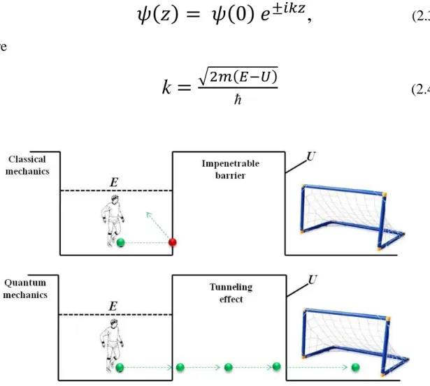
In classical mechanics, the electron in a potential U (z) is described by
(2.1) Where m is the electron mass, and E is the energy. In regions where E > , the electron has a non-zero momentum p 1/2, electron cannot penetrate into any region if E or a potential barrier.
In quantum mechanics, the electron described by a wavefunction (z), which satisfies Schrödinger equation,
(2.2) Consider the case of constant potential, as shown in Figure 2.2 in the classically allowed region E > , Eq. 2.2 has solutions
,
(2.3)Where
k
(2.4)
Figure 2.3 The difference between classical theory and quantum theory.
18
The momentum of electrons moving in positive and negative direction is constant momentum p = k and constant velocity V=p/m as the classical mechanics case. Eq. 2.2 in classical forbidden region has a solution.[3]
,
(2.5)
k
(2.6)
Where k is the decay constant.
The basic features of metal-vacuum-metal tunneling in a model as shown in Figure 2.2, the work function ɸ of a metal is defined as the minimum energy needed to remove one electron from the bulk to the vacuum level. The work function depends on the crystallographic orientation of the surface as well as the material. Suppose that the thermal excitation is negligible, the Fermi level is the upper limit of the occupied states in a metal where the vacuum level is the reference point of energy, simply discussion, the work functions of the tip and the sample are equal, EF = - ɸ. The electron can tunnel from the sample to the tip at the same time, the electron can tunnel from the tip to the sample surface.
A net tunneling current occurs after applying a bias voltage V. The sample state n with energy level En lying between EF – eV and EF has a chance tunneling into the tip. If V is so small compare to the work function, means that eV ɸ. Then the energy levels of the sample states are very close to the Fermi level, that is, En -ɸ. So the transmission coefficient T, which is the ratio of the tunneling current at the tip surface z to the impinging current at z = 0,
T
(2.7)
k
(2.8)
where k is the decay constant of the sample state near the Fermi level in the barrier region. [3]
19
2.2 Fabrication of molecular layers on silicon substrates in ultrahigh vacuum
A great development in the growth of ultrathin organic films and multilayer structure specially in the optoelectronic properties. There are several mechanisms to grow the organic molecules thin films depending on the nature and the structure of this molecule and the expectation model of its thin film layer. Ultrahigh vacuum (UHV) is one of the most important conditions to fabricate monolayer using special techniques such as Langmuir-Blodgett film and self-assembled monolayer from solution.[4-8] In addition, organic molecular beam deposition (OMBD) and organic molecular beam epitaxy (OMBE) usually done in UHV conditions which have many advantages in the fabrication process of organic thin film such as control the layer thickness and clean the substrate and environment in atomic scale.
As explained before, the reconstructed Si(001)-(2×1) surface with Si-Si dimers is a good substrate which can react withπbonds of unsaturated organic molecules to fabricate well-ordered organic films with novel physical properties. Thus, many reports show that it is possible to use reactions between the oriented dimers present on the Si(001) surface and the double bonds present in unsaturated organic molecules and align them in ordered translationally and rotationally.
Under UHV conditions, Hamers et al.[9, 10] built an STM system with base pressure 1x10⁻¹⁰ Torr to observe the adsorption of cyclopentene and 1,5- cyclooctadiene to fabricate a well-defined interface between silicon and organic molecular layers that are ordered translationally and rotationally. The rotational orientations of the molecules arise from the directional interaction of the π orbitals of the starting alkene with the π orbital of the dimers comprising the reconstructed Si(001) surface. The Si(001) surface act as the guide for determining the directionality and the ordered structure of the molecules of
20
organic film. These molecules bind via a cycloaddition reaction, producing ordered films at 300 K. The use of bifunctional compounds such as 1,5- cyclooctadiene which push the orientation of the C=C bond in the monolayer film to be extended into subsequent layers then forming multilayer anisotropic organic films. This kind of reactions which involves covalent bonding without dissociation lead to a high degree of molecular order even at room temperature.
The uniform spacing between dimers of the Si(001) surface leads to translational order of the molecular overlayer.
21
References
1) G. Binnig, H. Rohrer, Ch. Gerber, and E. Weibel, Appl. Phys. Lett. 40 (1982) 178.
2) G. Binnig, H. Rohrer, Ch. Gerber, and E. Weibel, Phys. Rev. Lett. 4 (1982) 57.
3) C. J. Chen, Introduction to Scanning Tunneling Microscopy, 2nd ed., Oxford University Press, New York (1993).
4) S. R. Forrest, P. E. Burrows, E. I. Haskal, and F. F. So, Phys. Rev. B 49 (1994) 11309.
5) M. Hara, H. Sasabe, A. Yamada, and A. F. Garito, Jpn. J. Appl. Phys. 28 (1989) L306.
6) A. Koma, Prog. Cryst. Growth Charact. 30 (1995) 129.
7) R. H. Tredgold, Order in Thin Organic Films, Cambridge University Press, Cambridge, 1994.
8) H. Hong, M. Tarabia, H. Chayet, D. Davidov, E. Z. Faraggi, V. Avny, R.
Neumann, and S. Kirstein, J. Appl. Phys. 79 (1996) 3082.
9) R. J. Hamers, J. S. Hovis, S.Lee, H.Liu, and J. Shan, J. Phys. Chem. B 101 (1997) 1489.
10) J. S. Hovis, H. Liu, and R. J. Hamers, Appl. Phys. A 66 (1998) s553.
22
3 Experimental Methods:
3.1 Substrate preparation: clean Si(001)-(2×1)surface
A huge number of scientific research and reports have been published to find the a convenient method to fabricate free defect clean Si(001) surface because the high concentration of defects on Si(001) surface control the morphology of the surface[1-12], and important processes, such as, the adsorption phenomena, thin films growth and oxidation process reflect disadvantages and make these processes worse.
The types and concentrations of defects depending on the fabrication methods of the sample and increasing the difficulty to compare the research results for different groups. The needed to find a solution to decrease the effect of Si(001) defects was observed and reported by many researchers, in addition finding a method to fabricate a surface free from defects in urgently and has been developed by several different approaches.
The defect free Si(001) act as a standard template for future surface science research and applications. The method of fabricating a defect free surface is needed to be able to be applied to any sample. Many different surfaces preparation methods to obtain clean Si(001) surfaces have been proposed, such as, chemical treatments and passivation.
Scanning tunneling microscopy is the standard probe to check the cleanness of the surface at high atomic resolutions, many preparation methods such as ion bombardment stopped, on the other hand annealing and flashing methods became the best choice to fabricate defect free Si(001) surface.
Nowadays, widely employed of annealing and flashing in fabrication clean Si(001) surface. Cleaning the sample holder material is one of the important conditions to fabricate clean Si(001) surface[13]. Our special method to fabricate clean Si(001) surface in UHV conditions is very simple and effective to reduce the different kinds of defects, such as missing atoms, split dimer and adsorbed contaminations shown in Figure 3.1 (a), (b) and (c) respectively.
23
Figure 3.1 STM images for clean Si(001) surface show examples of (a) the missing atoms defects, (b) spilt dimmers defects , and (c) adsorbed contaminations defects.
(b)
(c)
(a)
24
In this study, we used a home-built ultrahigh vacuum (UHV) STM system with a base pressure of 2 × 10-11 Torr operated at RT. The system has a sample preparation chamber with a base pressure on the order of 10-10 Torr.
A cut of 2×12×0.35 mm3 from a B-doped Si(001) wafer with a resistivity of 0.01-0.02Ω∙cm was used as a substrate. The substrate was cleaned by ultrasonic bath of acetone and ozone cleaner (NL-UV253, Nippon Laser &
Electronics Lab) to remove organic and metal contaminations.
The Si samples were clamped to a Ta holder by Ta clips with great care of handling using ceramics tolls without touching any metal parts Next, the substrate was introduced to the main chamber, followed by resistively using our special method for degassing, flashing and annealing processes.
The difficulties to use thermocouple for measuring the temperature during flashing and annealing process so the temperature was measured by a pyrometer shown in Figure 3.2.
25
Figure 3.2 (a) top view of the setup of the pyrometer in front of the window to the heat stage (b) front view of the pyrometer focusing to the sample surface.
Window to sample heat stage
Si sample
(a)
Pyrometer
(b)
26
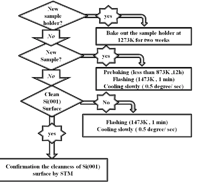
Next, the substrate was introduced to the main chamber followed by resistively heating, using our special flowchart to fabricate defect free Si(001) surface shown in Figure 3.3. If the sample holder is new, degassing at 1273K for two weeks is required to remove the contaminations covered the sample holder material.
The next step, if the sample is new so degassing at 873 K for 12 h and subsequent flashing at 1473K for 1 min to degas the Hydrogen, Oxygen and carbohydrates and organic contaminations. Finally, coaling the sample to room temperature(RT) at a rate of about 0.5 degree/sec to reconstruct the Si atoms to (2x1) structure and reducing the missing atoms and split dimmers defects , then confirming the cleanness of Si(001)-(2×1)surface using STM, if the cleanness and the free defect surface not confirmed so repeating flashing at 1473K for 1min and coaling the sample to RT at a rate of 0.5 degree/sec is required to confirm the cleanness and defect free Si(001)-(2×1) surface.
27
Figure 3.3 flaw chart describing the total process to fabricate a defect free Si(001)-(2×1) surface step by step.
28
3.2 DAT deposition on Si(001) at low coverages
After confirmation the cleanness and defect free Si(001)-(2×1) surface by STM technique in the main chamber, sample became ready to work as a substrate for DAT molecules adsorption process, then the sample has been transferred to the preparation chamber using control rods, the preparation chamber was equipped with a molecule deposition apparatus (Figure 3.4 (a)) consisting of a tungsten carbide crucible wounded with a sheath heater with a thermocouple, a water cooling jacket, and a mechanical shutter between the crucible and a substrate. The crucible temperature was controlled by a digital controller (LT350, CHINO Corp.).
DAT was purchased from Lancaster Synthesis and used after purified three times by train sublimation method.[14] (DAT purification process explained in details at the attached appendix). The DAT was evaporated by heating the crucible containing the DAT at a temperature ranged from 418 to 433 K, which was below the DAT melting temperature of ~510 K, accompanied by a rise of pressure below 10-9Torr in the preparation chamber (Figure 3.4 (b)).
The substrate temperature was RT (not controlled intentionally). The DAT coverage was monitored by a quartz thickness monitor (CRTM-9000, ULVAC, Inc.), and controlled by the mechanical shutter from a few seconds to a few minutes, by controlling the opening time of the shutter with a certain flux, we can control and calibrate the depositing amount, after finishing the depositing process, sample has been transferred to the preparation chamber using the control rods through the gate between the depositing chamber and preparation chamber then transferred again to the STM main chamber through the gate between the preparation chamber and main chamber, then confirm the depositing process and observe the phenomena of DAT configurations on Si(001) surface using STM .
29
Figure 3.4 (a) the depositing apparatus and (b) model of the depositing process.
DAT Source Sample Surface
Stopwatch Sample
holder
Sample surface DAT
Source
shutter Transfer
rod
30
The STM images were acquired at a constant current of 0.05 to 0.1 nA and a tip bias voltage of +1.5V (filled state). Furthermore, we annealed the samples at a substrate temperature of 423 for 10 min by passing a DC current into the substrate after DAT deposition to examine the change in DAT configuration on the Si(001) surface.
31
3.3 Model calculation of DAT on Si(001)
Oda et.al. [15], conducted the density functional theory (DFT) calculations for stable configurations of DAT on a Si(001)-(2×1) surface with the tilted angles between DAT molecules and Si(001) dimer lines at 17°and 0°
after our request depending on our experimental results, the DFT calculations done for three deferent configurations, the first one non adsorbed DAT molecule have a separated distance to Si(001) surface, and two adsorbed configurations 0° and 17°, because the separation distance between DAT and Si(001) surface in the non-adsorbed model case, so the interaction between DAT and silicon atoms can be neglected (Figure 3.5).
Figure 3.5 Schematic diagram of non-adsorbed model.[15]
32
So, the total energy of the non-adsorbed model to 0.0 eV. The total energy for configuration at 17° and 0° was -2.34 eV and -1.66 eV, respectively, referring to the total energy of 0.0 eV for a system consisting of a Si(001)-(2×1) surface and a DAT molecule separated from the surface. The difference in the total energy by 0.68 eV indicates that the configuration of DAT at 17° was stable. Figure 3.6 and Figure 3.7 show the models of DAT configurations at 17°
and 0° respectively, which were reproduced from the optimized configurations in ref.15.
From the chemical configuration, the stability at 17° is related to three chemical bonds to the Si surface: each of two amino groups at both ends of a DAT covalently bonds to a Si atom of a dimer, and the center benzene ring forms a butterfly-like bond [16] with a Si dimer.
Noted that the two amino groups are bonded to respective Si atoms on the opposite sides of the same dimer row. Consequently, since the DAT takes the so- called butterfly configuration of a double arch shape on the Si(001) surface For a model of the DAT with the tilted angle of 0° (Figure 3.6), while the two amino groups at both ends of the DAT are bonded to respective Si atoms on the one side of a Si dimer row, there is no butterfly-like bond, resulting in an upward arch of the main framework of the DAT. Accordingly, the protrusion with the tilted angle of 0°
33
Figure 3.6 Schematic diagram of 0° configuration model.[15]
34
Figure 3.7 Schematic diagram of 17° configuration model.[15]
35
3.4 Preparation and evaluation of STM tungsten tips
We demonstrated the liquid metal electrode method to reproducibly fabricate a sharpened W tip for STM. We can make the metal wire in contact with the liquid metal electrode in low stress but in good electric contact, leading to less mechanical tear-off. An elongated sharp W tip with a diameter of 100 nm over a length of 1 µm was formed; this is preferable to apply the build-up process to prepare an atomically sharpened tip for STM.[17]
3.1.1 Introduction of preparation of electrochemical etching of W tip STM is powerful to observe surface topography on an atomic scale using tunneling current depending on the separation between a sample and a sharpened tip in close proximity [18]. Since the spatial resolution of STM is dominated by the sharpness of the tip, a number of methods to fabricate a sharpened tip were reported [19–23].
In general, the STM tips are made by electrochemical etching of various metal wires [24] : for example, W [25], Ni [26], Co [27], Pt, Ir, Au, Pd, Rh [28];
in these reports apparatuses for electrochemical etching were developed to obtain sharpened tips. Development of methods to prepare tips with controllable profiles by electrochemical etching has continued for a wide variety of technical applications including electron emitter, ion-beam emitter, point contacts in conductance measurements, etc.
The conditions for electrochemical etching were systematically examined using a metal ring electrode to obtain better profiles of the tip, while the tension on the wire affected the sharpness of obtained tips [29]. A small contact potential difference between the wire and the electrode also changed the blunt shape of the tip [30]. Furthermore, by applying pulse trains of bias voltage between the wire and the electrode using a function generator, the tip profiles were controlled owing to anion distribution change surrounding the wire in an electrolyte solution [31].
In order to prepare tips in desired profiles, there has still been room to be
36
examined in electrochemical etching methods. In this study, a novel method is presented to fabricate a sharpened tip with an elongated shank by electrochemical etching using liquid metal gallium (Ga) as an electrode without specific electronic circuits.
The one end of wire is in touch to the liquid metal electrode with a good electrical contact due to its wettability and lightly supported with damping by its viscosity, which prevents the wire from mechanically tearing-off. The electrochemical etching is automatically stopped just after the wire breaks into two pieces, resulting in leaving a sharpened tip end. The tips prepared by this method are examined by scanning electron microscopy (SEM) and field emission microscopy (FEM), and used in STM observation.
3.1.2 Preparation method
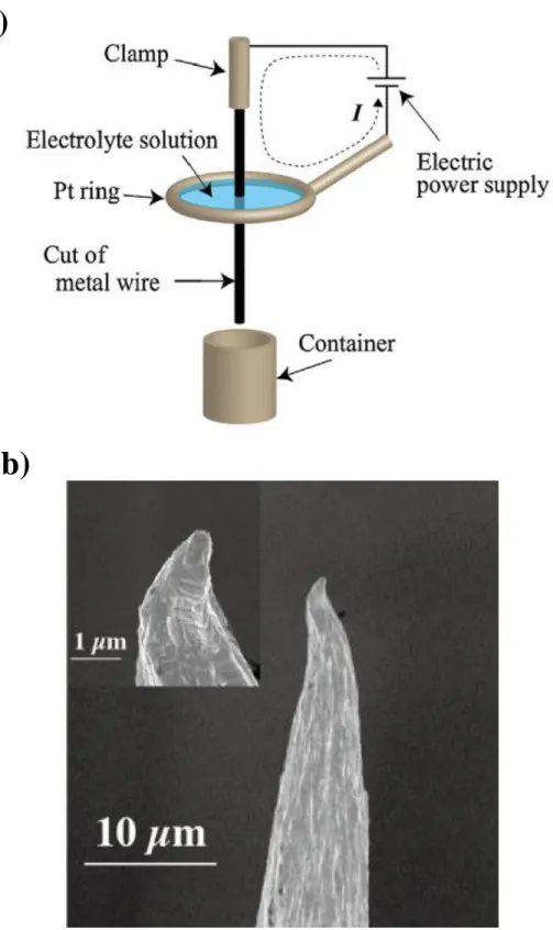
First, a typical setup for electrochemical etching of the tip is shown in Figure 3.8(a), which was used before in our lab. A ring of Pt wire was placed horizontally, in which an electrolyte solution was held in meniscus under surface tension onto the ring. A cut of metal wire for the tip was inserted into the solution by pinching its top end with a metal clamp.
As the etching progressed by passing current between the ring and the clamp, a part of the metal wire immersed in the solution became thin, and finally broke into two pieces; both of which were used for an STM tip. To catch the dropped piece, a receiver of a small tubular container was placed under the wire. Immediately after the wire broke into the two pieces, the electrochemical etching for the dropped piece automatically stopped, because this piece came off from the loop of etching current through the Pt ring, the solution, the clamp, and an electric power supply.
To quickly drop the piece from the solution to avoid further chemical corrosion in the etching solution, a long cut of metal wire or a weight was attached at the bottom of the wire [27,32]. There was, however, a tendency that the end of broken piece exhibited slightly rugged after the piece was torn off;
37
the wire broke into the two pieces before the thinning part was completely electrochemically etched. An example of a bent tip mechanically torn-off in the setup is shown in SEM images in Figure 3.8(b).
38
Figure 3.8 (a) Schematic of a typical setup to fabricate STM tips by electrochemical etching in a meniscus solution in a Pt ring. (b) SEM image of a bent tip of polycrystalline W wire prepared using this setup, as an example.
Inset shows a magnified image of the tip.
(a)
(b)
39
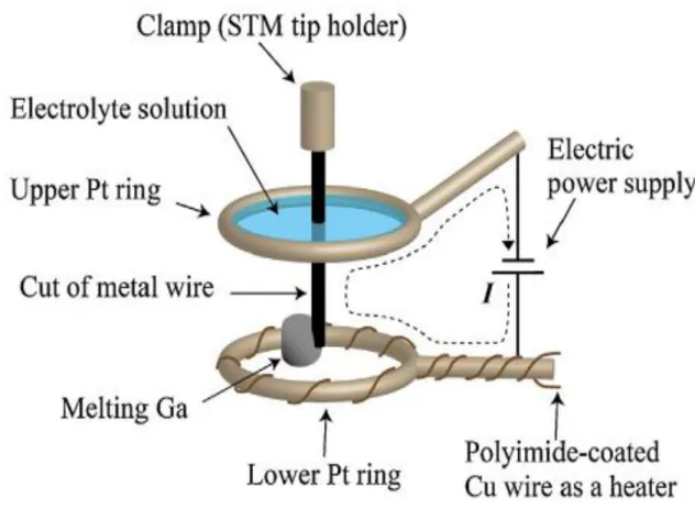
Next, the schematic diagram of the present setup developed in this study and its photos are shown in Figure 3.9 and Figure 3.10, respectively. This apparatus is similar to that shown in Figure 3.8, except for the bottom part, where the cut of metal wire is in contact with a liquid metal electrode of Ga having high wettability to the wire. Mercury (Hg) is also usable as a liquid metal electrode but should be avoided because of the toxicity of Hg. A Pt wire of ring was wounded with a polyimide-coated Cu fine wire of 0.15 mm in diameter, which was employed as a small heater, shown in Figure 3.10(b).
At first we soaked the Pt ring in a melting Ga lump slightly heated at a temperature higher than the Ga melting temperature of 29°C, and pulled up the ring from the lump, resulting in a film of Ga held onto the ring. To keep the Ga film in a liquid state, a current of about 0.2 A at 0.1 V into the Cu wire was passed to heat it above 29°C. A cut of metal wire for the tip was inserted into the liquid metal film, and the film was broken. Subsequently, the Pt ring, on which the small droplets of liquid Ga remained, was positioned to touch the bottom of the wire to the droplet, shown in Figure 3.10(c). The droplet can maintain the contact with the surface tension and viscosity of melting Ga. Then, the wire was held in very low stress and in good electric contact with the Pt ring at the bottom of the wire. In our practical way, the cut of the wire was mounted on a tip holder of STM, located at the top of Figure 3.9 (the detail is not shown), after the wire was spot welded to a metal loop of W wire; the loop was used to heat the tip in ultra-high vacuum (UHV) for degas and build-up process by passing current into the loop and applying a high voltage before STM observation, as mentioned in experiment section. When the wire was electrochemically etched, the wire pointed downward, penetrated the film of etching solution in the upper Pt ring, and the bottom end of the wire touched the liquid metal electrode on the lower Pt ring. When the electrochemical etching was completed, that is, the wire split into two pieces, the circuit of electrochemical etching of the upper piece opened instantaneously, and no
40
further etching current passed to the upper piece. Thus, no additional switching circuit was required to stop the etching current. Since the upper piece was mounted on the STM tip holder, the tip for STM observation can be used immediately without resetting it into other holders. In practice, an overplus lengthy part of the wire, about 10 mm longer than a finally desired length as the STM tip, was required for the etching. In the case of a shorter metal wire used in this etching process, an additional length of wire was attached at the end of the metal wire with a bit of silver paste; the bottom of additional wire was in contact with the liquid metal electrode.
Figure 3.9 Schematic of the setup of electrochemical etching with a liquid metal electrode.
41
Figure 3.10 (a) Pt wire ring, (b) Pt wire of the ring is wounded with a polyimide-coated Cu fine wire of 0.15 mm in diameter as a heater, and (c) photo of the setup with a Pt ring (upper) and a Pt ring wounded the Cu wire (lower) covered with liquid metal Ga.
(c)
42
A [111]-oriented single crystal W rod (FEI Company) of 0.13 mm in diameter was used to prepare an STM tip using the setup shown in Figure 3.2.
The rod was electrochemically etched in a solution of 4 mol/l KOH at a DC voltage of 3 V applied to the rod, and split into the two pieces in about 5 min.
Subsequently, the upper piece on the STM tip holder was soon retracted and used in the following experiments. After the tip was rinsed in hot water and ethanol to remove salt residues out of the etching solution, the tip was observed by SEM and FEM. A field emission SEM (S-5200, Hitachi High-Technologies Corporation) and a home-made FEM combined with a home-made STM operated in a UHV chamber with a base pressure of 2 × 10⁻¹¹ Torr were used;
FEM/STM observations and tip treatments were conducted in the same stage without tip transfer [33–35]. Before the FEM observation the tip was heated at about 600°C for 6 h in the UHV chamber to remove overlayers covering the tip.
Furthermore, the tip was treated to be sharpened in a build-up process of applying 3 kV and simultaneously heating at about 2000°C by passing an AC current into the W loop as a thermal field treatment [35]; the W atoms on the tip apex are polarized owing to the high electric field and diffuse at the high temperature toward the apex of the [1 1 1] direction at higher electric field, resulting in a sharper end of the tip. Using the treated tip, STM images of a clean Si(1 1 1) − 7 × 7 and a Si(0 0 1) − 2 × 1 reconstructed surface were observed, which were prepared by flashing at 1250 °C in the UHV chamber.
43
3.1.3 Evaluation of Preparation of law stress electrochemical etching of W tip
Figure 3.11 shows SEM images of the W tip electrochemically etched using the setup in Figures. 3.9 and 3.10. The tip radius was evaluated to be less than 20 nm within the accuracy limited by a narrow focus depth of the SEM (S- 5200) for the three dimensional shape of the tip and by the growth of contamination layers deposited with a focused electron beam at high magnification. Just after etching current was shut off, the tip end was probably sharper than 20 nm; the radius of tip apex slightly became larger owing to overlayers growth such as oxides covering the tip apex while being transferred in air. The diameter of the shank was less than about 100 nm over a length of 1 m from the tip end, which looks elongated compared with that fabricated by conventional etching methods. This elongated fine shank indicates that use of the liquid metal electrode reduces the effect of tear-off during the electrochemical etching. The tip was treated in the build-up process in the UHV chamber and observed by FEM [36]; a typical FEM image obtained after the treatment is shown in Figure. 3.12(a), which was observed at an applying voltage of −1.0 kV. The [1 1 1]-oriented W tip has a three-fold symmetry in crystallography, and a facet of (1 1 1) at the center and three facets of {013}
around the (1 1 1) facet on the tip end have work functions lower than those of the other facets, from where electrons are easily field-emitted.
Consequently, FEM images of a dull tip of [1 1 1]-oriented W usually show a bright wide pattern around the center of a FEM screen with three-fold symmetry. For facetted sharper tips prepared by applying a high voltage at a high temperature the FEM patterns show one bright spot at the center of the image, corresponding to the field emission from the [111]-oriented protrusion, accompanied by three bright spots surrounding the center spot with the three- fold symmetry, corresponding to the <013>-oriented protrusions.
44
Figure 3.11 (a) SEM image of a W tip fabricated in the procedure using the liquid metal electrode. (b) Magnified SEM image of the apex in (a).
(b)
(c)
45
On the other hand, in the FEM image in Figure 3.12, we observed only one prominent bright spot of the [111]-oriented protrusion at the center after an optimizing build-up process [33]. This indicates that the W tip atomically protruded to only the [111] direction of the tip axis; a small pyramidal atomic structure as a protrusion to the [111] orientation was probably formed, as shown in Figure 3.12(b).The build-up process of the tip was achieved reproducibly and easily with the tip fabricated in the process using the liquid metal electrode. It is probable that the fine tip elongated over 1 µm, as shown in Figure 3.11 of the SEM image, is preferable to carry out the build-up process, because the high electric field is easily concentrated at the apex of the elongated tip.
46
Figure 3.12 (a) FEM image at -1.0 kV of a build-up W tip fabricated in the procedure using the liquid metal electrode. A faint bright arch on upper right is the discharge of peripheral area of a micro-channel plate with a phosphor screen for FEM. (b) model of a [111]-oriented build-up W tip surrounded with facets of {110} and {211}. The confined sharp region of (111) plane with a low work function, depicted in green at the center, can easily field-emit electrons, which corresponds to the bright spot at the center in (a).
47
Figure 3.13 STM images taken with W tips fabricated using the liquid metal electrode.(a)STM imageof a Si(111)-7×7 surface; scanning area:
about 18 nm × 27 nm, tunneling current: 0.05 nA, tip voltage: -1.5 V.
(b)Si(001)-2×1 surface; scanning area: about 36 nm × 38 nm; tunneling current: 0.1 nA, tip voltage: 1.5 V.
48
Using this tip after the FEM observation we brought the tip closer to sample surfaces and succeeded in observing stable atom-resolved STM images of Si(111)-7×7 and Si(001)-2×1,as shown in Figure 3.13. Using the method with the liquid metal electrode demonstrated in this study, we can prepare an elongated W tip with a diameter less than 100 nm and as long as 1 µm. It is expected that the diameter of the thinning elongated part can be as small as 1 nm just before the wire is split. Since the Fermi wavelength of metals is of the order of Å, the quantum mechanical quantized conductance [35] may emerge in the thinning part. The quantized conductance was reported by methods of electroplating combined with etching [36], mechanically controlled break junctions [37], STM [38]and so on.
Those methods were applied to detection of quantized conductance for soft or polycrystalline metals such as Au, but not for brittle metals as W. It is worth while pointing out that this method using the liquid metal electrode is applicable to the formation of a fine wire of brittle metals where the conductance is quantized due to the quantum mechanical effect. The conductance in the wire even during etching is possibly detected by electrochemical techniques using a potential stat or a lock-in amplifier with AC modulation to separate the electrochemical etching current.
49
References
1) R. J. Hamers and U. K. Kohler, J. Vac. Sci. Technol. A 7(1989) 2854 . 2) K. Hata, M. Ishida, K. Miyake, and H. Shigekawa, Appl. Phys. Lett. 73, (1998) 40.
3) M. Uchikawa, M. Ishida, K. Miyake, K. Hata, R. Yoshizaki, and H.
Shigekawa, Surf. Sci. 357 (1996) 469 .
4) R. A. Wolkow, Phys. Rev. Lett. 68 (1992) 2636.
5) H. Tochihara, T. Amakusa, and M. Iwatsuki, Phys. Rev. B 50 (1994) 12262.
6) K. Hata, T. Kimura, Y. Sainoo, K. Miyake, R. Morita, M. Yamashita, and H. Shigekawa, Jpn. J. Appl. Phys., Part 1 38 (1999) 2904.
7) T. Yokoyama and K. Takayanagi, Phys. Rev. B 56 (1997) 10483.
8) T. Yokoyama and K. Takayanagi, Phys. Rev. B 57 (1998) 4226.
9) A. R. Smith, F. K. Men, K.-J. Chao, and C. K. Shih, J. Vac. Sci. Technol.
B 14 (1996) 914.
10) H. Shigekawa, K. Miyake, M. Ishida, K. Hata, H. Oigawa, Y. Nannichi, R. Yoshizaki, A. Kawazu, T. Abe, T. Ozawa, and T. Nagamura, Jpn. J.
Appl. Phys., Part 2 35 (1996) L1081.
11) H. Shigekawa, K. Hata, K. Miyake, M. Ishida, and S. Ozawa, Phys. Rev.
B 55 (1997) 15448.
12) H. Shigekawa, K. Miyaka, M. Ishida, and K. Hata, Jpn. J. Appl. Phys., Part 1 36 (1997) L294.
13) V. A. Ukraintsev, Z. Dohnalek, and J. T. Yates, Jr., Surf. Sci. 388 (1997) 132.
14) H. J. Wagner, R. O. Loutfy, and C. K. Hsiao, J. Mater. Sci.17(1982)2781.
15) M. Oda, Phys. Status Solidi C9 (2012) 1443.
16) F. Y. Naumkin, J. C. Polanyi, D. Rogers, W. Hofer, and A.Fisher, Surf. Sci.
547 (2003)324.