Cells Fabricated by Wet Process
著者 モハマド シャヒドゥザマン
著者別表示 MD Shahiduzzaman journal or
publication title
博士論文本文Full 学位授与番号 13301甲第4480号
学位名 博士(学術)
学位授与年月日 2016‑09‑26
URL http://hdl.handle.net/2297/46583
Creative Commons : 表示 ‑ 非営利 ‑ 改変禁止 http://creativecommons.org/licenses/by‑nc‑nd/3.0/deed.ja
FABRICATED BY WET PROCESS
A DISSERTATION
SUBMITTED TO THE DIVISION OF MATERIAL SCIENCE IN PARTIAL FULFILLMENT OF THE REQUIREMENTS FOR THE
DEGREE OF DOCTORATE IN PHILOSOPHY
by
MD. SHAHIDUZZAMAN
REGISTRATION NO.: 1323132008 ADVISOR: DR. TETSUYA TAIMA
GRADUATE SCHOOL OF NATURAL SCIENCE & TECHNOLOGY DIVISION OF MATERIAL SCIENCE
KANAZAWA UNIVERSITY KAKUMA, KANAZAWA, JAPAN
SEPTEMBER, 2016
FABRICATED BY WET PROCESS
Ph.D. THESIS
by
MD. SHAHIDUZZAMAN
GRADUATE SCHOOL OF NATURAL SCIENCE & TECHNOLOGY DIVISION OF MATERIAL SCIENCE
KANAZAWA UNIVERSITY KAKUMA, KANAZAWA, JAPAN
SEPTEMBER, 2016
Dissertation
Investigation of Nanoparticles and Interface Effects on Organometal Halide Perovskite Solar Cells Fabricated by Wet Process
Graduate School of Natural Science & Technology Kanazawa University
Major Subject: Division of Material Science
School Registration No.: 1323132008 Name: Md. Shahiduzzaman
Chief Advisor: Associate Professor Tetsuya Taima
i
Hybrid organometal halide perovskites such as methylammonium lead iodide (CH3NH3PbI3) are attracting considerable attention as energy-efficient light absorber materials for photovoltaic applications owing to their solution processability, tunable bandgap, strong absorption coefficients, and cost effectiveness. The control of morphology and crystallization are the main challenges encountered in perovskite-based thin films and affect the quality of the resulting film. We have approached new method to tune morphology of perovskite and applied interlayer control method in order to improve power conversation efficiency (PCE) of perovskite solar cells. This thesis presented two different approaches, which are aimed at contributing to the development of planar heterojunction (PHJ) perovskite solar cells.
(1) We prepared CH3NH3PbI3 nanoparticles (NPs) for the first time using a simple spin- coating method by incorporating a small amount (1~10 wt %) of an ionic liquid (IL) 1- hexyl-3-methylimidazolium chloride in 25 wt % solution of CH3NH3PbI3 in N,N- dimethylformamide (DMF) onto the compact-TiOx/ITO substrates to control size and shape of NPs. Compact-TiOx films were prepared by chemical bath deposition (CBD) according to the procedure described by Kuwabara et al. (Organic electronics 11, 2010, 1136). The CH3NH3PbI3 NP thin films were uniform and free of pin holes, and the excellent morphology was due to the addition of IL. The small-sized CH3NH3PbI3 NPs (~350 nm) with superior optical absorption properties have been obtained with 3 wt % of IL in the medium, as compared to the other compositions with wt % of 1, 7 and 10. As a result, a maximum PCE of 2.81% was obtained with the solar cell using 3 wt % of IL in a solution. The effect of viscosity of varying ILs have also been investigated. Low viscosity of ILs together with completely dissolve in CH3NH3PbI3 solution were playing a significant role in controlling the morphology of resulting NPs.
The preliminary results are promising for the fabrication of PHJ solar cells based on CH3NH3PbI3 NPs using a device configuration of ITO/TiOx/ CH3NH3PbI3 NPs/ spiro- OMeTAD/Ag. We also expect that the results will open a pathway towards a better understanding for the fabrication, modification and enhancement of the performance of
ii
performances due to the residual IL content remained on the CH3NH3PbI3 NP films.
(2) Taima et al. (Jpn. J. Appl. Phys. 54, 2015, 08KF05) have developed interlayer control method and employing it in efficient polymer based organic solar cells.
Considering this, I have applied this method to PHJ perovskite solar cells.
We fabricated PHJ type perovskite solar cells with enhanced efficiency by introducing fullerene (C60) interlayers with thicknesses of 0, 3, 7 and 10 nm between air- stable amorphous compact TiOx and CH3NH3PbI3 layers. The modified morphology obtained by inclusion of C60 improved the surface energy properties of the cells in terms of enhanced photocurrent. Atomic force microscopy (AFM) verified the correlation between the surface energy and phase morphology of the PHJ solar cells. The introduction of a C60 interlayer between CH3NH3PbI3 and TiOx layers increased the content of photogenerated charge carrier sites, as well as lowering the accumulation and trapping of photogenerated charges at the TiOx interface. The optimum thickness of C60
interlayer was 7 nm, for which a maximum PCE of 9.51% was obtained.
Keywords: Nanoparticles; Ionic liquid; Spin-coating method; Organometal halide perovskite; CH3NH3PbI3; Interlayer; Fullerene (C60).
iii
iv
gratitude to my respected supervisor Dr. Tetsuya Taima, Associate Professor, Institute for Frontier Science Initiative (InFIniti), Kanazawa University, Japan for his highly valued supervision, solemn instruction, constructive criticism, valuable suggestions and constant encouragement during the entire period of this research work and in the preparation of this dissertation.
I cherish the desire to thank Dr. Kohshin Takahashi, Professor, Graduate School of Natural Science and Technology, Kanazawa University, Japan for inspiring me to do very hard work on research during my doctoral study.
I accord my heartily reverence to Dr. Takayuki Kuwabara, Associate Professor, Graduate School of Natural Science and Technology, Kanazawa University, Japan for his whole-hearted co-operation, encouragement and enthusiastic suggestion throughout my research work.
I would like to acknowledge to Dr. Makoto Karakawa, Associate Professor, Institute for Frontier Science Initiative (InFIniti), Kanazawa University, Japan for his inspiration and co-operation.
I express my sincere gratitude to the former and current members of the Taima and Takahashi Lab for their support and sharing with me the studying time in the lab.
I would like to thank Dr. Mahabubur Rahman for his kind advice and inspiration of my research of the doctoral program.
My thanks will go to Dr. Mizanur Rahman for his encouragement and advice from the beginning of my research in JAPAN.
I highly acknowledge Dr. Ismail Md. Mofizur Rahman for his kind support and help during my doctoral study.
I am especially indebted to my wife Nayeema Afroz Sultana for her tireless help and heartiest co-operation that kept and keeping me focused to the objective.
I also would like to thank my parents, parents-in-law, brothers and sisters for their endless love and understanding for all hard and happy moment of my life.
In fine, all praises go to Almighty Allah, the omniscient and the most merciful.
Md. Shahiduzzaman September 2016
v
vi
Dedicated to
My Parents, parents-in-law, and beloved wife
vii
viii i) Abstract
iv) Acknowledgements viii) Table of Contents
xi) Abbreviation and Symbol xv) List of Figures
xix) List of Tables
CHAPTER ONE: GENERAL INTRODUCTION TO ORGANOMETAL HALIDE
PEROVSKITE SOLAR CELLS ...1
1.1 Perovskite and Perovskite Solar Cells ...2
1.1.1 Working principal of perovskite solar cells ...4
1.1.2 Notable achievements to date ...5
1.1.3 Photovoltaic efficiency records ...6
1.1.4 Commercialization challenges ...8
1.2 Solar Cells Characterization ...9
1.2.1 Reference solar spectral irradiation ...9
1.2.2 Current-voltage characteristics ...10
1.2.3 Quantum efficiency measurements ...11
1.3 Review on Perovskite Nanoparticles Solar Cells ...12
1.3.1 Fabrication method of perovskite nanostructures...14
1.3.1.1 Spin-coating method ...14
1.3.1.2 Slip-coating method ...18
1.3.1.3 Chemical vapor deposition (CVD) method ...19
1.4 Conclusions ...20
1.5 Future Outlook ...20
CHAPTER TWO: IONIC LIQUID-ASSISTED GROWTH OF METHYLAMMONIUM LEAD IODIDE SPHERICAL NANOPARTICLES BY A SIMPLE SPIN-COATING METHOD AND PHOTOVOLTAIC PROPERTIES OF PEROVSKITE SOLAR CELLS ...23
2.1 Introduction ...23
2.2 Experimental ...25
2.2.1 Chemicals ...25
2.2.2 Instrumentation ...26
2.2.3 Methods ...26
2.2.3.1 Substrate cleaning ...26
2.2.3.2 Preparation of compact-TiOx films by chemical bath deposition (CBD) ...27
2.2.3.3 Preparation of MAPbI3 NCs by spin coating ...27
2.2.3.4 Preparation of MAPbI3 NPs by spin coating ...27
ix
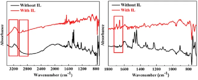
2.3.2 Existence of IL within the NP film confirmed by FTIR-analysis ...37
2.3.3 Formation mechanism of MAPbI3 films and photovoltaic properties ...38
2.3.4 A non-destructive solvent-assisted washing procedure for preparing CH3NH3PbI3 NP films. ...40
2.4 Conclusions ...41
CHAPTER THREE: SHAPE-CONTROLLED CH3NH3PBI3 NANOPARTICLES FOR PLANAR HETEROJUNCTION PEROVSKITE SOLAR CELLS ...43
3.1 Introduction ...43
3.2 Experimental ...46
3.2.1 Preparation of compact-TiOx films by CBD ...46
3.2.2 Solar cells device fabrication ...47
3.3 Results and discussion ...48
3.3.1 Chemical structure of IL and mixture solution of CH3NH3PbI3 and IL ...48
3.3.2 The general concept of IL used as a morphology controller ...49
3.3.3 Size and shape control of perovskite NPs films ...49
3.3.4 Effect of annealing temperature on the NPs properties ...51
3.3.5 Composition of NPs ...53
3.3.6 Crystallinity, FTIR spectra, and absorption of Perovskite NPs ...54
3.3.7 Calculation of viscosity of IL-DMF liquid solution ...58
3.3.8 Proposed formation mechanism and photovoltaic properties of perovskite NPs ...59
3.4 Conclusions ...62
CHAPTER FOUR: VISCOSITY EFFECTS OF IONIC LIQUIDS AS ADDITIVE ON CH3NH3PBI3 NANOPARTICLES AND THEIR PHOTOVOLTAIC PROPERTIES ...64
4.1 Introduction ...64
4.2 Experimental ...67
4.3 Results and discussion ...68
4.3.1 Chemical structures of ILs ...68
4.3.2 Morphology ...69
4.3.3 X-ray diffraction analysis ...71
4.3.4 FTIR analysis ...72
4.3.5 UV-vis analysis ...74
4.3.6 Photovoltaic properties ...76
4.4 Conclusions ...77
CHAPTER FIVE: ENHANCED PHOTOVOLTAIC PERFORMANCE OF PEROVSKITE SOLAR CELLS VIA MODIFICATION OF SURFACE CHARACTERISTICS USING A FULLERENE INTERLAYER ...80
5.1 Introduction ...80
5.2 Experimental ...82
5.2.1 Preparation of compact-TiOx films by chemical bath deposition (CBD): ...82
x
materials ...85
5.3.2 Fabrication steps of PHJ perovskite solar cells ...87
5.3.3 Morphology and crystallinity ...87
5.3.4 Contact angle measurements and the relationship between photovoltaic properties and surface energy ...90
5.3.5 Photovoltaic Characterization ...93
5.4 Conclusions ...97
REFERENCES………100
APPENDIX A: LIST OF PUBLICATIONS ...112
xi
CH3NH3PbI3 Methylammonium lead iodide PHJ Planar heterojunction
NP, NPs Nanoparticle, Nanoparticles nm nanometer
IL Ionic liquid wt% Weight percent
DMF N,N-dimethylformamide CBD Chemical bath deposition PCE Power conversion efficiency
Spiro-OMeTAD 2,2’,7,7’-tetrakis(N,N-di-p-methoxyphenylamine)-9,9’- spirobifluorene
CO2 Carbon dioxide OPV Organic photovoltaic DSSCs Dye sensitized solar cells HTM Hall transporting material ETA Electron transporting activity ITO Indium tin oxide
ZnO Zinc oxide CuI Cupper iodide
CuSCN Copper (I) thiocyanate
NREL National renewable energy laboratory ASTM American society for testing and materials AM0 Air Mass Zero
AM1.5G Reference solar spectral irradiance of ASTM G-173-03 EQE External quantum efficiency
xii
SEM Scanning electron microscopy NW, NWs Nanowire, Nanowires
MAI Methylammonium iodide IPA Isopropanol
MAPbI3 Methylammonium lead iodide TiO2 Titanium dioxide
3D Three-dimensional
HRTEM High resolution transmission electron microscopy FFT Field effect transistor
UV-Vis Ultraviolet-visible Al2O3 Aluminium oxide
AFM Atomic force microscopy IoT Internet of Things
HMImCl 1-hexyl-3-methylimidazolium chloride PbI2 Lead iodide
TiOSO4 Titanium (IV) oxysulfate H2O2 Hydrogen peroxide
EDX Energy-dispersive X-ray spectroscopy XRD X-ray diffraction
FTIR Fourier Transform Infrared Spectroscopy IRRAS Infrared Reflection Absorption Spectroscopy RMS Root mean squire
RT Room temperature [TBAM][CL] Tetrabutylammonium chloride
[BMIM][CL] 1-benzyl-3-methylimidazolium chloride
xiii
[EMIM][TFSI] 1-ethyl-3- methylimidazolium bis (trifluoromethanesulfonyl) imide
[DMIM][CL] 1, 3-didecyl-2-methylimidazolium chloride [P6,6,6,14][DCA] Trihexytetradycyl phosphonium dicyanamide PCBM [6,6]-phenyl-C61-butyric acid methyl ester LUMO Lowest unoccupied molecular orbital HOMO Highest occupied molecular orbital C60 Fullerene
FF Fill factor
Symbol
μL Microliter Pa Pascal
J-V Current densities versus voltage Jsc Short-circuit current density Voc Open-circuit voltage
η Viscosity ηIL Viscosity of IL
Mole fraction of DMF
M Molar h Hour eV Electro volt ( ) / ° Contact angle
xiv
JMPP Voltage maximum power point VMPP Current maximum power point
xv
Figure 1.1. Schematic illustration of perovskite crystal structure………...3 Figure 1.2. Schematic of the working principle of a perovskite solar cells…...4 Figure 1.3. Solar cells efficiency chart……….………..7 Figure 1.4. Solar irradiation spectrum………..………..9 Figure 1.5. Schematic illustration of current-voltage measurement of a solar cells…….10 Figure 1.6. Plane-view SEM images of MAPbI3 NWs formed by two-strep spin coating method using the solution of MAI in IPA (35 mg/5 mL) with (a) 10 μL of, (b) 50 μL of DMF, (c) 100 μL of DMF, and (d) without DMF. MAPbI3 was deposited on a 100 nm thick mesoporous TiO2 (diameter of about 40 nm) layer. Scale bars represent 1 μm (200 nm in insets). Reprinted with permission from ref. 49. Copyright 2015, ACS………...……….……15 Figure 1.7. HRTEM images of individual nanoparticles from POA2 (a and c) and their corresponding FFT analyses (b and d). Reprinted with permission from ref. 50. Copyright 2014, ACS……….16 Figure 1.8. High-resolution SEM images for CH3NH3PbBr3 nanoparticles. Left image:
bare Al2O3 surfaces. Right image: deposited CH3NH3PbBr3 crystals prepared with 1 wt%
precursor solution. Reprinted with permission from ref. 52. Copyright 16- 093….………..………..17 Figure 1.9. Schematic illustration of the low temperature slip-coating process for the fabrication of filiform lead-methylamine iodide perovskite thin films (a−c). Photo of the coating formed on a microscope glass slide (d). Optical microscopy image of filiform crystallites grown on SiO2/Si substrate (e). Reprinted with permission from ref. 53.
Copyright 2015, ACS ...…...18 Figure 1.10. Morphological characterizations of lead halides nano-platelets as-grown on muscovite mica substrate: a) Optical (above) and SEM (below) images of lead halides:
A,D: PbCl2; B,E: PbBr2; C,F: PbI2. Reprinted with permission from ref. 54. Copyright 2014, WILEY.………..……….19 Figure 1.11. Schematic diagram of powering IoT devices at all hours………21
xvi
Figure 2.2. The low- and high-magnification SEM images of MAPbI3 films prepared without IL (a, b) and with IL (c, d), respectively………...31 Figure 2.3. AFM images of MAPbI3 films prepared by spin coating (a) without and (b) with the addition of IL to control morphology; (c) air-stable uniform compact TiOx film prepared by CBD; (d) MAPbI3 small clusters prepared at RT………..32 Figure 2.4. (a) The dark field images of MAPbI3 film formed without IL and EDX mapping of (b) lead and (c) iodine (10 µm scale bar for all); (d) the dark field images of MAPbI3 film formed with IL and EDX maps of (e) lead and (f) iodine (2.5 µm scale bar for all)………33 Figure 2.5. The XRD patterns of MAPbI3 films formed with (red color) and without IL (black color)………..35 Figure 2.6. The UV-Vis spectra of only IL and MAPbI3 films prepared with and without IL. Inset photographs show MAPbI3 films prepared with (left) and without (right) IL…36 Figure 2.7. The FTIR spectra of MAPbI3 films with and without IL………...37 Figure 2.8. Schematic of the formation mechanism of MAPbI3 NPs………...39 Figure 2.9. (a) Device structure of solar cells based on MAPbI3; (b) The J-V characteristics obtained for the solar cells based on MAPbI3 with and without IL……..40 Figure 2.10. Schematic illustration of solvent additive procedure for preparing MAPbI3
NP film………..41 Figure 3.1. (a) Chemical structure of 1-hexyl-3-methylimidazolium chloride (HMImCl), (b) Homogeneous mixture solution of CH3NH3PbI3 and IL………49 Figure 3.2. The SEM images of the CH3NH3PbI3 NPs prepared in the presence of varying concentration of IL: (a) 1 wt %, (b) 3 wt %, (c) 7 wt %, and (d) 10 wt %...50 Figure 3.3. The AFM images of (a) TiOx film; (b) As-deposited CH3NH3PbI3 small clusters prepared at RT and CH3NH3PbI3 NPs with varying concentration of IL: (c) 1 wt
%, (d) 3 wt %, (e) 7 wt %, and (f) 10 wt %...51
xvii
Figure 3.5. (a) The dark field images of CH3NH3PbI3 NP formed with 1 wt % IL and EDX mapping of (b) lead and (c) iodine (10 µm scale bar for all); (d) the dark field images of CH3NH3PbI3 NP formed with 3 wt % IL and CH3NH3PbI3 EDX maps of (e) lead and (f) iodine (2.5 µm scale bar for all); (g) the dark field images of CH3NH3PbI3
NP formed with 7 wt % IL and EDX maps of (h) lead and (i) iodine (5 µm scale bar for all)………..54 Figure 3.6. The XRD patterns of CH3NH3PbI3 films processed with varying wt % of IL………55 Figure 3.7. The FTIR spectra of CH3NH3PbI3 NPs film………..56 Figure 3.8. The UV-Vis spectra of the CH3NH3PbI3 films processed with varying wt % of IL as well as only IL. Inset photographs show CH3NH3PbI3 films prepared with varying concentration of IL: (a) 1 wt %, (b) 3 wt %, (c) 7 wt %, and (d) 10 wt %...57 Figure 3.9. Schematic illustration of formation mechanism of CH3NH3PbI3 film in (a) DMF-only and DMF-IL system……….60 Figure 3.10. (a) Device configuration of solar cells based on CH3NH3PbI3 NPs; (b) The J-V characteristics obtained for the solar cells based on CH3NH3PbI3 NPs………..61
Figure 4.1. Chemical structure of different ILs of (a) [TBAM][CL], (b) [AMIM][CL], and (c) [BMIM][CL]; (d) mixture solution of CH3NH3PbI3 and 3 wt % of IL………….68 Figure 4.2. AFM images of (a) Perovskite film without IL and CH3NH3PbI3 NPs in the presence of varying ILs: (b) [TBAM][CL], (c) [BMIM][CL], and (d) [AMIM][CL]…...70 Figure 4.3. XRD patterns of CH3NH3PbI3 NPs films processed with different ILs…….71 Figure 4.4. The FTIR spectra of CH3NH3PbI3 NPs film………..73 Figure 4.5. UV-vis spectra of CH3NH3PbI3 NPs films processed with different ILs…..75 Figure 4.6. (a) Device configuration of CH3NH3PbI3 NPs solar cells; (b) The J-V characteristics achieved for the solar cells based on CH3NH3PbI3 NPs………76
xviii
Figure 5.2. Presents schematic illustration of the device structure of PHJ perovskite solar cells………85 Figure 5.3. Lowest unoccupied molecular orbital (LUMO) and highest occupied molecular orbital (HOMO) energy levels of the materials and work functions of ITO and Ag electrodes in the perovskite hybrid solar cells……….86 Figure 5.4. Schematic diagram of PHJ perovskite solar cells………..87 Figure 5.5. The AFM images of (a) TiOx film; and C60 with varying thickness (nm): (b) 3, (c) 7, and (d) 10……….88 Figure 5.6 The AFM images of the perovskite film prepared in the presence of varying C60 thickness (nm): (a) 0, (b) 3, (c) 7, and (d) 10………..88 Figure 5.7. XRD patterns of CH3NH3PbI3 films with and without a C60 interlayer…...90 Figure 5.8. Optical images of the contact angles of a (a) TiOx film, and C60 layers with a thickness of (b) 3, (c) 7, and (d) 10 nm………..91 Figure 5.9. Characteristics of CH3NH3PbI3 solar cells as a function of the surface energy of the C60 layer: (a) short-circuit current density, Jsc, (b) open-circuit voltage, Voc, (c) fill factor, FF, and (d) power conversion efficiency, PCE. Error bars show plus-or-minus one standard deviation from the mean………..93 Figure 5.10. J-V characteristics of the device with and without C60 interlayer for different thicknesses………...95 Figure 5.11. Incident photon to current conversion efficiency (IPCE) spectra of the device with and without C60 interlayer for different thicknesses………...96
xix
NPs/Spiro-OMeTAD/Ag………...61
Table 4.1. Viscosity measurement data for different ILs (3 wt %) in DMF……….74 Table 4.2. Performance of cells with the structure ITO/compact-TiOx/CH3NH3PbI3
NP/Spiro-OMeTAD/Ag……….76
Table 5.1. Contact angles and surface energy values………92 Table 5.2. Performance of cells with the structure ITO/compact-TiOx/C60 or CH3NH3PbI3/Spiro-OMeTAD/Ag………...97
xx
Chapter One:
General Introduction to Organometal Halide Perovskite Solar Cells
“I’d put my money on the sun and solar energy. What a source of power! I hope we don’t have to wait until oil and coal run out before
we tackle that.”
- Thomas Edison, March 19311
Energy is taken into account to be the blood of the planet owing to the actual fact that all activities of physical object require energy. There are two types of energy sources, including long run energy (eternal energy) such as solar energy or earth heat, and the other created from alternative energy and preserve in biomass and endured a chemical and physical transition like charcoal, petroleum, fossil fuel…These all energy sources will be ready to use subsequently, but it can be expected to run out quickly in the long run at the present demand of energy. Moreover, using these energy sources continuously leads to the CO2 emission that damages the surroundings and sustainable development.
Therefore, considering sustainable environment, a replacement strategy and research should be devoted to solve the energy and environmental issues. All over the world,
researchers are doing their best to choose green energy sources broadly and practically obtainable to switch using oil and charcoal.2, 3
Solar cells can be used as a potentially alternative energy source that are able to directly convert the incident solar radiation into electricity, together with no noise, pollution or moving parts, making them robust, reliable, and long lasting. Solar cells provided long-duration power supply effectively for satellites and space vehicles.4
The majority of research on solar cells focused on silicon-based assemblies, which is used as light absorber and the charge transporter. However, the high processing costs and toxicity of the chemicals that have been involved in the preparation scheme discouraged its wide application. Although researchers are working to minimize the issues, there have been continuous efforts on developing solar cells using alternative materials, mostly using organic components, such as, perovskite and dye-sensitized solar cells (DSSCs).5 Hybrid organometal halide perovskites exhibit considerable attention as energy-efficient light-absorbing materials for photovoltaic applications due to strong absorption coefficients, long electron-hole diffusion lengths, tunable band gap, high charge carrier mobilities, solution processable, and cost-effective.6-9
1.1 Perovskite and Perovskite Solar Cells
Perovskite has been considered as a calcium titanium oxide (CaTiO3) mineral that named as Russian Geographical Society founder Lev Perovskiti. The general chemical formula of perovskite structure refers to ABX3 that has the same crystallographic structure as perovskite (mineral). The large inorganic atomic cation B (positively charged
cations) occupied in the center of a cube and faces of the cube area unit engaged by a small atom X (negative charge anion).
Organometal halide perovskite solar cells devices are produced with the following combination of materials:
A = Organic cation - methylammonium (CH3NH3)+
B = Inorganic cation - lead (Pb2+)
X3= Halogen anion – chloride (Cl-)/ iodide (I-) Perovskite crystal structure is shown in Fig. 1.1.
Figure 1.1. Schematic illustration of perovskite crystal structure
Among organic-inorganic perovskite-structured semiconductors, most common light-absorbing material is methylammonium lead iodide (CH3NH3PbI3). It has high charge carrier mobility and lifetime in which allowing light-generated electrons and holes to transport far enough distances to be extracted as current, in terms of losing their energy as heat within the cell.10
1.1.1 Working principal of perovskite solar cells
Figure 1.2 present the schematic illustration of the working principle of a perovskite solar cells. In the case of following perovskite solar cells, electron transporting layer and hole transporting layer can be referred as ETL and HTM, respectively. Indium tin oxide (ITO)-patterned glass substrates are used as a conducting transparent electrode. Gold (Au) is also used as a contact electrode.
Figure 1.2. Schematic of the working principle of a perovskite solar cells
Working principle of perovskite solar cells consist four steps: light absorption, charge separation, charge transport, and charge collection. Light travelling through conducting transparent electrode onto a perovskite layer (photosensitive layer) to generate excitations named as electron-hole pairs (e–/h+). The charged molecules (electron-hole) diffuse and separate through the charge-conducting layers to their corresponding electrodes, thus producing electricity. Organometal halide perovskite
(CH3NH3PbI3) exhibits itself both electron and hole properties. Hence, perovskite solar cells can be fabricated both as p-n and p-i-n junction. Perovskite solar cells are usually involved with two structures such as mesoporous and planar heterojunction. Mesoporous metal oxide (e.g., Al2O3, TiO2) layer usually is used to collect more electrons. High temperature processing is required to fabricate mesoporous layers. On the contrary, planar heterojunction cells have attracted more interest for flexible solar cells since their fabrication does not require high-temperature process.
1.1.2 Notable achievements to date
The efficiency of perovskites as a light-absorber material with 3.8%11 power conversion efficiency (PCE) was first reported by Kojima in 2009. Park et al.12 have further improved the PCE to 6.5% in 2011. Park, Grätzel and colleagues reported perovskite solar cells with a PCE of 9.7%13 was fabricated by introducing spiro- OMeTAD as a hole transporting material (HTM). Almost at the same time, Snaith et al.14 also reported perovskite solar cells together with spiro-OMeTAD. The combined efforts of Seok and Grätzel group15 reported PCE of 12% using nanoporous TiO2 scaffolding.
The further enhanced efficiency of 12.3% reported using similar structures and mixed- halide CH3NH3PbI3−xBrx perovskites16. Improved morphology was obtained using two- step method and TiO2 scaffolding by Grätzel group.17 Snaith et al. showed similar results without using TiO2 scaffolding. Liu et al. reported planar heterojunction solar cells with efficiency of 15.7% by employing ZnO nanoparticle layer18 as electron collection layer (ECL). Notable perovskite solar cells performance has also been achieved by using inorganic HTM such as CuI19 and CuSCN.20 An efficiency of 15.6%21 has been obtained
by employing low-temperature processed ECL of graphene/TiO2 nanocomposites.
Furthermore, efficiency of 15.9%22 has been achieved by combining tiny TiO2
nanoparticles along with a titanium diisopropoxide bis(acetylacetonate) binder perovskite solar cells. Besides, Yang et al.23 reported with a PCE of 19.3% was fabricated by employing interface engineering.
During the past few years, the encouraging discovery has been continued further to achieve a notable 22.1% conversion efficiency until the date24, and will be expected to rise towards 25% in the near future25. Noticeably, the perovskites provide a promising pathway to explore next-generation photovoltaic together with higher performance of solar cells.
1.1.3 Photovoltaic efficiency records
The prompt performance enhancement of organometal halide perovskite solar cells have opened a new pathway to rising star of the photovoltaics world and showed interest to the academic research community. Figure 1.3 presented a graph that used the information from National Renewable Energy Laboratory (NREL) solar cells efficiency chart.
Figure 1.3. Solar cells efficiency chart
This graph showed the comparison of conversion efficiency over the recent years between perovskite solar cells and other technologies. The encouraging discovery of perovskite solar cells will be continued to rise further remarkable performances over the coming years.
1.1.4 Commercialization challenges
The present performance of perovskite solar cells showed a promising interest of multiple attempts to commercialize photovoltaic products in upcoming years. The high- performance perovskite solar cells contained a key component of lead (Pb) that could be influenced against the taking care of such products in consumer.
In terms of cost, perovskites may compete with CdTe photovoltaic thin-film solar cells. The higher-performance of perovskites have typical drawbacks together with CdTe, specifically dependence on an environmentally hazardous heavy metal. Currently, photovoltaic modules are released from the regulation of European Union on the use of Restriction of Hazardous Substances (RoHS), at least for large, fixed, professionally installed systems.
Without this exemption, CdTe solar cell modules would have no risk that met the demand of RoHS. The maximum permitted concentration of products, which is limited to 0.01% or 100 ppm for cadmium (Cd) by weight in any uniform layer. Considering the CdTe modules, perovskite modules may be promising of multiple attempts to commercialize in upcoming years because the RoHS limit on Pb in a uniform layer is ten times higher than that of Cd.
1.2 Solar Cells Characterization
1.2.1 Reference solar spectral irradiationSolar spectrum is the most important aspects of solar cells characterization that is engaged to evaluate the performance of a photovoltaic device. Solar spectrum irradiance is standardized by the American Society for Testing and Materials (ASTM). The spectrum outside zero atmosphere is referred to as Air Mass Zero (AM0). By employing AM0, satellites and high-flying aircraft are usually characterized. The AM0 can be considered for the extraterrestrial irradiance. Figure 1.4 showed that the solar radiation spectrum.26 The integrated spectral irradiance is 1366.1 W/m2 for the standardized of AM0.
Figure 1.4. Solar radiation spectrum
Solar irradiance is reduced due to absorption and scattering processes, while passing through the atmosphere. The Earth surface receiving solar spectrum irradiance is defined by the ASTM G-173-03 named as AM1.5G. This represents the solar zenith
angle of 48.19°, which is corresponding to an Air Mass of 1.5 and for specific atmospheric conditions. The integrated spectral irradiance is 1000.4 W/m2 for the standardized of AM1.5G.
1.2.2 Current-voltage characteristics
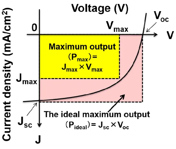
Current density versus voltage (J–V) characteristics of the photovoltaic devices are measured at AM 1.5G illumination (Fig. 1.5) in order to evaluate of the solar cells performance.
Figure 1.5. Schematic illustration of current-voltage measurement of a solar cells
The short-circuit current density (Jsc) is the current density through the solar cells, while the voltage of solar cells is zero (mAcm-2). Jsc is directly depend on the light intensity (number of photons). The open-circuit voltage (Voc) is the maximum voltage from a solar cells device, when the current is zero (V). The current density at the time of the maximum output of the element (mAcm-2) is defined as Jmax. The aximum output when the voltage of the device (V) is also defined Vmax, The maximum output of the element Pmax: Pmax = Jmax × Vmax (wcm-2). The energy of the incident light (AM1.5G) E = 100 (mWcm-2). Fill factor (FF) is referred as the ratio of the maximum power of the solar cells to the product of Voc and Jsc.
Fill factor (FF) = Jmax×Vmax/(Jsc×Voc)………..1.1
Power conversion efficiency (PCE) is also referred as the ration of solar-energy output from the solar cells to input energy from the sun. From the I-V curve, all the parameters such as Jsc, Voc, FF, and PCE are determined.
Power Conversion Efficiency (PCE)
= Pmax/E
= Jmax×Vmax/E
= (Jsc×Voc)×FF/E……….1.2
1.2.3 Quantum efficiency measurements
The term quantum efficiency (QE) of a solar cell is measured in terms of a function of wavelength and represents the fraction of an incident photons that converted into
electrons of the external circuit. Two types of QE of a solar cells are existed: the external quantum efficiency (EQE) and the internal quantum efficiency (IQE). The EQE is also defined as the incident photon-to-electron conversion efficiency (IPCE), considering the number of photons that are emitted from the solar simulator and that hit the photosensitive area of the solar cells. IPCE value depends on the absorption of light (photons) and the collection of charge carriers. When a photon has been absorbed and has generated an electron-hole (e-/h+) pair, these charge carriers will be separated and collected at the interface of the junction. Charge recombination can be avoided to have good devices. Charge recombination influences a drop in IPCE. The IPCE value is calculated with the known photon flux J0 of the solar simulator according to Equation 1.3, where Jsc is the short-circuit current density and e the elementary charge.
IPCE = Jsc/eJ0………....1.3
1.3 Review on Perovskite Nanoparticles Solar Cells
Hybrid organometal halide perovskite solar cells have made an impressive improvement in the last couple of years, mainly by their high PCE over 22% until the date. Perovskites have also shown potential for application in various fields like superconductors,27 sensors,28 fuel cells,29 ferroelectric,30, 31 photocatalysis,32 batteries,33, 34 and thermoelectrics.35 Semiconductor nanostructures have opened the door for the utilization of nanocrystalline pigments as enticing light-weight harvesters, that have the subsequent characteristics: a) The nanostructure of the light absorbent material layer possesses sub-wavelength features attributable to quantum size effects, which results in
very low reflection and accumulated photon absorption and provides higher cell efficiency without the necessity for additional antireflection coatings; b) The large surface areas of nanotextured materials permit efficient energy conversion and charge–
carrier recombination.36 Among semiconductive materials, low-dimensional layered compounds are intensely investigated as a promising candidate for organic–inorganic- based perovskites.37 Complex-shaped perovskite nanoparticles (NPs) is one-dimensional (nanowires, nanotubes, and nanorods), two-dimensional (nanodiscs, nanoplatelets, and nanosheets), or alternative complicated nanostructures shapes including rod-sheet heterogeneous NPs, for example.
Up to now, there are several reports on quantum wells,38, 39, wires 40, and dots 41 synthesized from organic-inorganic perovskite compounds. Whereas varied synthetic approaches are used to prepare nanoscale perovskite materials, those supported chemical synthesis provide the foremost versatility in terms of the manipulation of the characteristics of individual particles, together with size, shape, and structure or surface properties.
Chemical synthetic techniques area unit advantageous for large-scale tailored production of anisotropic perovskite NPs, which may be promptly assembled into nanostructured bulk perovskite materials with highly efficient properties for practical applications. Many chemical synthetic strategies are developed to organize complex- shaped metal perovskite NPs, as well as the hydrothermal/ solvothermal techniques 42-44 and wet chemical synthesis45 method are frequently used. On the other hand, researchers
are interested in developing thin-film perovskite materials by easy, efficient, and precise techniques as an alternate to chemical synthesis.
In this review, we would like to overview of the perovskite nanostructures based solar cells from the following aspects: perovskite nanostructures fabrication method, and their physical properties. Future outlook for perovskite nanostructures as an energy harvesters will also be briefly discussed.
1.3.1 Fabrication method of perovskite nanostructures 1.3.1.1 Spin-coating method
Spin coating is a common, cheap, simple, and precise film production method, in which a centrifugal force is used to produce uniform solution-processed thin films.
Centrifugal force causes a dispersion to spread uniformly across a substrate, which is followed by evaporation of the solvent to yield a thin particle film.46 Shahiduzzaman et al.47, 48 reported the preparation of CH3NH3PbI3 NPs for the first time using a simple spin-coating method by incorporating a small amount (1~10 wt %) of an ionic liquid (IL) 1-hexyl-3-methylimidazolium chloride in 25 wt % solution of CH3NH3PbI3 in N,N- dimethylformamide (DMF) onto the compact-TiOx/ITO substrates. The CH3NH3PbI3 NP thin films were uniform and free of pin holes, and the excellent morphology was due to the addition of IL. The small-sized CH3NH3PbI3 NPs (~350 nm) with superior optical absorption properties have been obtained with 3 wt % of IL in the medium, as compared to the other compositions with wt % of 1, 7 and 10. As a result, a maximum PCE of 2.81% was obtained with the solar cell using 3wt % of IL in a solution.
Recently, Im et al.49 stated an efficient CH3NH3PbI3 (MAPbI3) nanowire (NWs) perovskite solar cells with the enhanced efficiency of 14.71% by employing two-step spin-coating technique as shown in Fig. 1.6a~d.
Figure 1.6. Plane-view SEM images of MAPbI3 NWs formed by two-strep spin coating method using the solution of MAI in IPA (35 mg/5 mL) with (a) 10 μL of, (b) 50 μL of DMF, (c) 100 μL of DMF, and (d) without DMF. MAPbI3 was deposited on a 100 nm thick mesoporous TiO2 (diameter of about 40 nm) layer. Scale bars represent 1 μm (200 nm in insets). Reprinted with permission.49 Copyright 2015, ACS.
As can be revealed from SEM images that the NW morphology completely depends on aprotic solvents and small quantity of DMF in IPA is confirmed to play a significant role in promoting growth of MAPbI3 peroskites. The NW film horizontal conductivity was higher than that of bulk cuboid film. The charge separation and conductivity is better in NW structure. Therefore, the higher device performance is expected for the uniform NW structured film.
Moreover, Schmidt et al.,50 demonstrated that the synthesis of methylammonium lead bromide (CH3NH3PbBr3) NPs with the diameter size of 6 nm by a straightforward spin-coating technique on a quartz substrate. The NPs were prepared simply by spin- coating technique that mixture of CH3NH3PbBr3 in the presence of oleic acid and octadecene as shown in Fig. 1.7. To isolate the NP core, the longer chain alkyl ammonium cation might play an significant role as a better capping ligand, while methylammonium cation with NPs might be helpful in the NPs based solar cell application.51
Figure 1.7. HRTEM images of individual nanoparticles from POA2 (a and c) and their corresponding FFT analyses (b and d). Reprinted with permission.50 Copyright 2014, ACS.
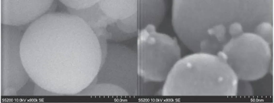
Kojima et al. 52 reported that the fabrication of CH3NH3PbBr3 NPs using a simple spin-coating technique by incorporating a (1~10 wt%) of precursor solution under UV- light irradiation onto a mesoporous media. The cross-section of high-resolution SEM images of Al2O3/CH3NH3PbBr3 film evidently shows CH3NH3PbBr3 NPs with the diameter of 5 nm were deposited on spherical Al2O3 as shown in Fig. 1.8. The Al2O3
paste was spin-coated onto a quartz glass substrate and annealed at 500 °C for 1 h. The resulting 1 µm thick amorphous film was obtained as confirmed by SEM observations.
Other semiconductor materials pastes such as SnO2, TiO2, and ZrO2 were prepared for comparison by using the same method. A precursor solution (CH3NH3Br and PbBr2 in DMF) was spin-coated on the Al2O3 film.
Figure 1.8. High-resolution SEM images for CH3NH3PbBr3 nanoparticles. Left image:
bare Al2O3 surfaces. Right image: deposited CH3NH3PbBr3 crystals prepared with 1 wt%
precursor solution. Reprinted with permission.52 Copyright 16-093.
1.3.1.2 Slip-coating method
CH3NH3PbI3 NWs with the diameter of 50 and 400 nm and length up to 10 µm were fabricated by a low-temperature solution process employing a slip-coating method.53 The small amount of spin-coating solution (CH3NH3PbI3 in DMF) was dropped onto a glass slide and covered it with a second microscope slide. The residual mixture solution formed a uniform liquid film between the glass slides (Fig. 1.9a−c). The 20 µL of the same saturated solution was applied to prepare thicker wires. Solvent evaporation from the uncovered surface resulted in an instantaneous yellow to brown-red color change. All the process were performed at room temperature.
Figure 1.9. Schematic illustration of the low temperature slip-coating process for the fabrication of filiform lead-methylamine iodide perovskite thin films (a−c). Photo of the coating formed on a microscope glass slide (d). Optical microscopy image of filiform crystallites grown on SiO2/Si substrate (e). Reprinted with permission.53 Copyright 2014, ACS.
1.3.1.3 Chemical vapor deposition (CVD) method
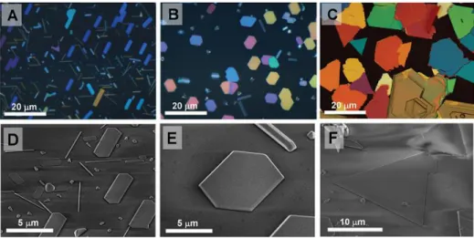
Ha et al.54 reported for the first time the fabrication of CH3NH3PbI3 nano-platelets with the dimension of 5-30 µm using van der waals epitaxial growth followed by thermally intercalating methylammonium halides on muscovite mica substrate. The growth of PbI2 nano-platelets was fabricated on muscovite mica substrate employing van der Waals epitaxy in a vapor transport chemical deposition system.55-57 After this, as- grown PbI2 nano-platelets are transformed to CH3NH3PbI3 by a gas–solid hetero-phase reaction in the presence of methylammonium halide molecules. Optical and SEM images of lead halides grown on muscovite mica substrate are shown in Fig. 1.10. Besides, the resultant CH3NH3PbI3 platelets with an electron diffusion length of over 200 nm fabricated by this promising method, which is approximately two twofold higher than the conventional solution spin-coating film.
Figure 1.10. Morphological characterizations of lead halides nano-platelets as-grown on muscovite mica substrate: a) Optical (above) and SEM (below) images of lead halides:
A,D: PbCl2; B,E: PbBr2; C,F: PbI2. Reprinted with permission.54 Copyright 2014, WILEY.
1.4 Conclusions
In this review, we have given an overview of the progress in nanostructured perovskite solar cells. Fabrication methods such as solution process, were shown to influence morphologies and crystal growth of the perovskite materials, thus impacting on the resultant energy conversion efficiency. The controlled morphologies of various perovskite nanostructures and their high electron mobility enable interfacial charge separation and fast electron transport which improve the charge collection efficiency in solar cells.
1.5 Future Outlook
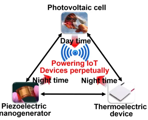
Energy harvesting is the process of electronically capturing and accumulating energy from a range of energy sources considered wasted or unusable for any practical purpose. Semiconducting CH3NH3PbI3 NPs are potential candidates for electronics and optoelectronics applications and can be highly efficient owing to its excellent electrical and optical properties, cost effectiveness, solution processability, tunable bandgap, and strong absorption coefficients. In order to get alternative power systems using ambient energy harvesting sources (radiant, thermal and mechanical) is a clear target for perpetual powering or recharging of the Internet of Things (IoT) devices as shown in Fig. 1.11. As for solar radiation, perovskite NPs based technology has the potential to increase solar conversion efficiency to more than 25 % in the very near future instead of 20 % for state- of-the-art cells. Solar energy can only be harnessed when it is daytime and sunny.
Therefore, harvesting ambient thermoelectric and piezoelectric nanogenerator energy
offers alternative solution to powering IoT devices and could provide enough energy to extend the lifetime of these devices. The large surface areas of nanostructured materials allow efficient energy conversion, and charge–carrier recombination.
Figure 1.11. Schematic diagram of powering IoT devices at all hours.
Hence, the development of energy harvesting technologies using CH3NH3PbI3 NPs is essential for powering the IoT devices perpetually.
<This page is intentionally left blank to indicate the chapter break>
Chapter Two:
Ionic liquid-assisted growth of methylammonium lead iodide spherical nanoparticles by a simple spin-coating method and photovoltaic properties of perovskite solar cells
The following chapter describes ionic liquid-assisted growth of CH3NH3PbI3 spherical nanoparticles employing a simple spin-coating technique and their use in perovskite solar cells.47
2.1 Introduction
Perovskites show potential for application in multiple fields such as superconductors,27 sensors,28 fuel cells,29 ferroelectric,30, 31 photocatalysis,32 batteries,33, 34 and thermoelectrics.35 Semiconductor nanostructures have opened the door for the use of nanocrystalline pigments as attractive light harvesters, which have the following characteristics: a) The nanostructure of the light absorber layer possesses sub-wavelength features because of quantum size effects, which results in very low reflection and increased photon absorption and provides higher cell efficiency without the need for additional antireflection coatings; b) The large surface areas of nanotextured materials allow efficient energy conversion and charge–carrier recombination.36 Among semiconducting materials, low- dimensional layered compounds have been intensely investigated as a promising candidate for organic–inorganic-based perovskites.37 Complex-shaped perovskite
nanoparticles (NPs) can be one-dimensional (nanowires, nanotubes, and nanorods), two-dimensional (nanodiscs, nanoplatelets, and nanosheets), or other complex shapes such as rod-sheet heterogeneous NPs. To date, there have been many reports on quantum wells,38, 39 wires,40 and dots41 synthesized from organic–
inorganic perovskite compounds. While numerous synthetic approaches have been used to prepare nanoscale perovskite materials, those based on chemical synthesis offer the most versatility in terms of the manipulation of the characteristics of individual particles, including size, shape, and structure or surface properties.
Chemical synthetic techniques are advantageous for large-scale tailored production of anisotropic perovskite NPs, which can be readily assembled into nanostructured bulk perovskite materials with highly efficient properties for practical applications.
Several chemical synthetic methods have been developed to prepare complex- shaped metal perovskite NPs, including the hydrothermal/ solvothermal method42-
44 and wet chemical synthesis.45 However, researchers are interested in developing thin-film perovskite materials by simple, cost-effective, and precise techniques as an alternative to chemical synthesis. Spin coating is a common, cheap, simple, and precise film production method, in which a centrifugal force is used to produce uniform solution-processed thin films. Centrifugal force causes a dispersion to spread uniformly across a substrate, which is followed by evaporation of the solvent to yield a thin particle film.46
Schmidt et al.,50 reported the synthesis of methylammonium lead bromide NPs by a simple spin-coating method on a quartz substrate with the objective of
fabricating nanostructured organic lead halide perovskite for use in the solar cells.
Moreover, MAPbI3 nanowires have been prepared by a low-temperature solution process using a simple slip-coating method53 for solar cells. Control of morphology and crystallization are the main challenges encountered in perovskite- based thin films and affect the quality of the resulting film. The morphology of non-homogeneous thin films can limit device performance because of electrical shorting, or effects on charge dissociation/transport/recombination.58-60 Therefore, an easy scalable efficient approach to fabricate homogeneous perovskite films with controlled morphology for use in perovskite solar cells needs to be developed.
In the present study, we use a simple spin-coating technique to fabricate uniformly distributed spherical NPs of MAPbI3 in the presence of the ionic liquid (IL) 1-hexyl-3-methylimidazolium chloride (HMImCl), which is introduced to control morphology. HMImCl has a high boiling point, extremely low vapor pressure, high ionic conductivity, and excellent electrochemical and high thermal stability.
2.2 Experimental
2.2.1 ChemicalsLead iodide (PbI2, purity 98%) was purchased from Tokyo Chemical Industry (Tokyo, Japan), while titanium (IV) oxysulfate (TiOSO4, purity 99.99) and 1- hexyl-3-methylimidazolium chloride (HMImCl, purity 97%) were from Sigma Aldrich (St. Louis, MO, USA). Hydrogen peroxide (H2O2, purity 35%) and N,N-
dimethylformamide (DMF, purity 99.5%) were supplied by Kanto Chemical (Tokyo, Japan).
2.2.2 Instrumentation
The scanning electron microscopy (SEM) and Energy-dispersive X-ray spectroscopy (EDX) (SU1510, Hitachi High-Tech, Tokyo, Japan) were used to analyse to analyse the surface morphology and elemental mapping. Surface morphology was further investigated by atomic force microscopy (AFM; SII SPI3800N, Seiko, Japan).
Ultraviolet-visible (UV-Vis) absorption spectra of perovskite films were measured using an absorption spectrophotometer (U-3310, Hitachi, Tokyo, Japan). X-ray diffraction (XRD) patterns of the prepared films were measured using an X-ray diffractometer (SmartLab, Rigaku, Japan) with an X-ray tube (Cu Kα, λ = 1.5406 Å). A further analysis of the films was performed using Fourier Transform Infrared Spectroscopy (FTIR) with Infrared Reflection Absorption Spectroscopy (IRRAS) (FT/IR-6300, Jasco, Tokyo, Japan).
2.2.3 Methods
2.2.3.1 Substrate cleaning
Indium tin oxide (ITO)-patterned glass substrates purchased from Techno Print Co., Ltd. (Saitama, Japan) were treated with oxygen plasma for 20 min prior to use.
2.2.3.2 Preparation of compact-TiOx films by chemical bath deposition (CBD)
Compact-TiOx layers were prepared in aqueous solutions of TiOSO4 (1.6 g) and H2O2 (0.17 g) at 80 °C via CBD.61, 62 The chemical bath was purchased from AS-One (EO-200, Tokyo, Japan). The deposited compact-TiOx films were heated on a hot plate (ND1, AS-One, Tokyo, Japan) at 150 °C for 1 h to obtain amorphous films.
2.2.3.3 Preparation of MAPbI3 NCs by spin coating
Lead iodide (PbI2) (0.144 g) and methylammonium iodide (MAI) (0.05 g) were mixed in anhydrous DMF (615 µL) at 2.89:1 molar ratio by shaking (VMR-5R, AS-One) at room temperature (RT) for 30 min to produce a clear MAPbI3 solution with a concentration of 25 wt %. PbI2 was dehydrated under vacuum at 450 °C for 3 h prior to use. Methylamonium lead iodide (MAI) was synthesized in our laboratory. A compact- TiOx layer (30 nm) was deposited on ITO-coated glass substrates using CBD technique as described earlier. The DMF solution of MAPbI3 (25 wt%) were spin coated on top of the amorphous compact- TiOx layer at 3000 rpm. During spin coating, the color of the film changed from transparent to peach. The film was left to dry at RT for 30 min to allow slow solvent evaporation, followed by annealing on a hot plate at 100 °C for 10 min, giving a MAPbI3 film with a thickness of 200 nm. The whole process was performed in an N2-filled glove box.
2.2.3.4 Preparation of MAPbI3 NPs by spin coating
MAPbI3 NPs were prepared using the same spin-coating technique as that described in preparation of MAPbI3 NCs, except that 1 wt % HMImCl was also included in the 25 wt % MAPbI3 solution in DMF.
2.2.3.5 Solar cell fabrication using MAPbI3 NPs
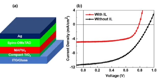
The hole-transporting layer (HTM) was produced using 2,2,7,7-tetrakis (N,N-di-p-methoxyphenylamine)-9,9-spirobifluorene (spiro-OMeTAD) via spin- coating at 4000 rpm over the MAPbI3 NPs layer. The spiro-OMeTAD in chlorobenzene (0.058 M) was prepared using 4-tert-butylpridine (0.19 M), and lithium bis (trifuluoro- methylsulfonyl) imide (0.031 M), tris [2-(1H-pyrazol-1- y1)-4-tert-butylpyridine] cobalt (III) tris [bis(trifluoromethysulfonyl) imide] (5.6 × 10⁻³ M) as dopants.63, 64 The films were left on a hot plate for annealing in the glove box at 70 °C for 20 min. The films were then placed in a vacuum chamber and 100 nm thick silver electrodes were deposited on the spiro-OMeTAD layer with a pressure at around 2.83 × 10⁻⁴ pa. The active device area was 4 mm2. The current densities versus voltage (J-V) characteristics of the cells were analyzed under simulated AM 1.5G solar illumination with Keithley 2401 Digital Source Meter.
2.3 Results and discussion
2.3.1 Morphology, composition, structure, and absorption of MAPbI3 NPs
The chemical structure of HMImCl is shown in Fig. 2.1a. We introduced 1 wt
% of HMImCl to the solution of MAPbI3 in DMF as a morphology-controlling additive. The IL-doped solution of MAPbI3 was a homogeneous clear yellow- orange, because no aggregate or NPs were observed in it (Fig. 2.1b). The process
used to fabricate MAPbI3 films with/without IL via spin coating is schematically illustrated in Fig. 2.1c.
Figure 2.2a–b reveal that the films processed without IL have incomplete surface coverage and are composed of non-uniform large crystals with a ribbon- like shape. These observations are similar to those in a previous report by Xiao et al.,65 which confirms that the non-uniformity in the perovskite film was caused by the rapid evaporation of DMF during spin coating. In contrast, uniform MAPbI3
NPs with a well-controlled spherical shape and an average diameter of 540 nm were observed when 1 wt% IL was added to the spin-coating solution (Fig. 2.2c–
d).
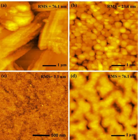
This observation is further confirmed by the AFM analysis (Fig. 2.3a, b). The Root-mean-square (RMS) roughness for the perovskite films with and without IL were, 23.4 and 76.1 nm, respectively. These data support the formation of a smooth uniform NP film by inclusion of an IL in the spin-coating solution.
Figure 2.1. (a) Chemical structure of HMImCl. (b) Photograph of a homogeneous solution of MAPbI3 in DMF containing 1 wt% IL. (c) Schematic of perovskite film formation with/without IL.
Figure 2.2. The low- and high-magnification SEM images of MAPbI3 films prepared without IL (a, b) and with IL (c, d), respectively.
A uniform air-stable amorphous TiOx layer with a thickness of 30 nm was prepared, as shown in AFM analysis (Fig. 2.3c). The RMS roughness of the amorphous film was 3.13 nm. The morphologies of the films produced at room temperature (RT) as determined by AFM (Fig. 2.3d). Figure 2.3d reveals that the small clusters formed at RT remained aggregated and was not uniformly distributed. The RMS roughness of the film was 46.5 nm as deposited film.
The EDX-mapping (Fig. 2.4a-f) was performed to address the question of whether the MAPbI3 films, processed with and without IL, are composed of single or multiple phases. The technique allowed us to visualize a two-dimensional map
of the relative location of the different elements in the sample. The color intensity assists to judge the relative amount of element distributed in the surface.
Figure 2.3. AFM images of MAPbI3 films prepared by spin coating (a) without and (b) with the addition of IL to control morphology; (c) air-stable uniform compact TiOx film prepared by CBD; (d) MAPbI3 small clusters prepared at RT.
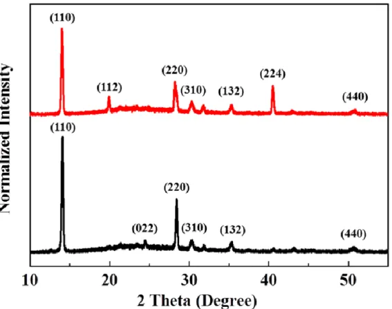
The EDX-analysis of MAPbI3 films showed mostly similar in both cases (with/without IL) the ratio Pb to I is around 21/64 in good agreement with a PbI3
stoichiometry.