INVITED PAPER
Special Section on Analog Circuits and Their Application TechnologiesDesign of Switched-Capacitor Voltage Boost Converter for Low-Voltage and Low-Power Energy Harvesting Systems
Tetsuya HIROSE†a),Member andYuichiro NAKAZAWA††,Nonmember
SUMMARY This paper discusses and elaborates an analytical model of a multi-stage switched-capacitor (SC) voltage boost converter (VBC) for low-voltage and low-power energy harvesting systems, because the output impedance of the VBC, which is derived from the analytical model, plays an important role in the VBC’s performance. In our proposed method, we focus on currents flowing into input and output terminals of each stage and model the VBCs using switching frequencyf, charge transfer capacitance CF, load capacitanceCL, and process dependent parasitic capacitance’s pa- rameterk. A comparison between simulated and calculated results showed that our model can estimate the output impedance of the VBC accurately.
Our model is useful for comparing the relative merits of different types of multi-stage SC VBCs. Moreover, we demonstrate the performance of a prototype SC VBC and energy harvesting system using the SC VBC to show the effectiveness and feasibility of our proposed design guideline.
key words: Internet of Things (IoT), energy harvesting, voltage boost con- verter, output impedance
1. Introduction
The development of ultra-low power LSIs is expected to lead to the expansion of the next-generation Internet-of- Things (IoT) era. IoT devices will be a promising commu- nication platform for collecting and delivering information throughout the world[1]–[8]. As shown in Fig. 1, a huge number of distributed IoT edge nodes will be installed ev- erywhere to measure various types of physical data in our surroundings, store and process the measured data, and out- put the data on demand. To realize such a society, IoT edge nodes must operate with low power because they will prob- ably be used under conditions where they have to draw nec- essary energy from poor, less-than-ideal energy sources.
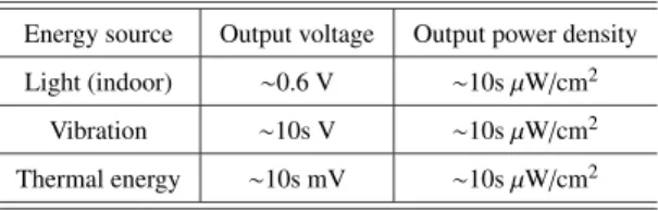
Energy harvesting has been studied and gained in- creasing attention as a means of enabling battery-less and maintenance-free systems[9]–[20]. Table 1 summarizes the typical characteristics of various energy sources. As shown in Table 1, the harvesters can supply approximately several tens of micro-watts. However, we cannot use the output voltages of the harvesters directly because they are too low to operate LSIs or battery chargers. Therefore, an ultra-low power and highly efficient power management circuit with a
Manuscript received March 22, 2020.
Manuscript revised March 23, 2020.
Manuscript publicized May 20, 2020.
†The author is with the Division of Electrical, Electronic and Information Engineering, Graduate School of Engineering, Osaka University, Suita-shi, 565–0871 Japan.
††The author is with Ricoh Electronic Devices Co., Ltd., Ikeda- shi, 563–0046 Japan.
a) E-mail: [email protected] DOI: 10.1587/transele.2019CTI0002
Fig. 1 IoT society with huge number of distributed edge nodes.
Table 1 Characteristics of various energy sources Energy source Output voltage Output power density Light (indoor) ∼0.6 V ∼10sμW/cm2
Vibration ∼10s V ∼10sμW/cm2 Thermal energy ∼10s mV ∼10sμW/cm2
voltage boost converter (VBC) is required.
As a VBC, switched capacitor (SC) VBCs are widely used to boost the output voltage of harvesters because the SC VBCs can convert a low-voltage input to a high-voltage output efficiently and can be implemented on a chip without using external off-chip components. In addition, a higher output voltage can be obtained easily by connecting SC VBCs in cascade[17]–[26].
Analytical models of multi-stage SC VBCs are use- ful for investigating and estimating the VBCs’ perfor- mance[27],[28]. Although conventional models using sim- ple SC VBCs have been discussed in[29],[30], few reports on a model using more practical SC VBCs can be found. In addition, although the conventional models use the switch- ing frequency f and flying capacitanceCFto model a VBC, a load capacitanceCLand complementary SC configuration are not taken into account. Therefore, the modeling accu- racy is insufficient for use in actual VBCs.
In this paper, we develop and elaborate an analytical model of a multi-stage VBC. In our model, we focus on currents flowing in input and output terminals of each stage, and then the output impedance is derived by using switching clock frequency f, charge transfer flying capacitorCF, and load capacitor CL. A complementary SC configuration is also taken into account. By deriving the output impedance of the VBC, we can estimate and design a highly efficient Copyright c2020 The Institute of Electronics, Information and Communication Engineers
HIROSE and NAKAZAWA: DESIGN OF SC VBC FOR LOW-VOLTAGE AND LOW-POWER ENERGY HARVESTING
447
multi-stage SC VBC. We also discuss the effect of non-ideal parasitic capacitance and resistance, and we conduct a dedi- cated performance comparison using ideal, short-, and long- channel MOS switches. Moreover, a prototype SC VBC and energy harvesting using the SC VBC are developed to show the effectiveness and feasibility of our proposed design guideline.
This paper is organized as follows: Sect. 2 describes the operation of the SC VBC. Section 3 explains our modeling method. The effects of parasitics on the SC VBC are dis- cussed and some key performance metrics are derived theo- retically. Section 4 shows the effectiveness of the model and demonstrates a prototype SC VBC and energy harvesting system using the SC VBC. Section 5 concludes the paper.
2. Switched-Capacitor VBC
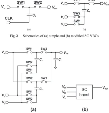
Figure 2 (a) shows a schematic of a simple SC VBC. It can generate an (n+1) times higherVout from an input voltage Vinby connecting n-stage SC VBCs in cascade. However, many stages are needed to generate a higherVoutbecause the clock (CLK) has the same voltage asVin.
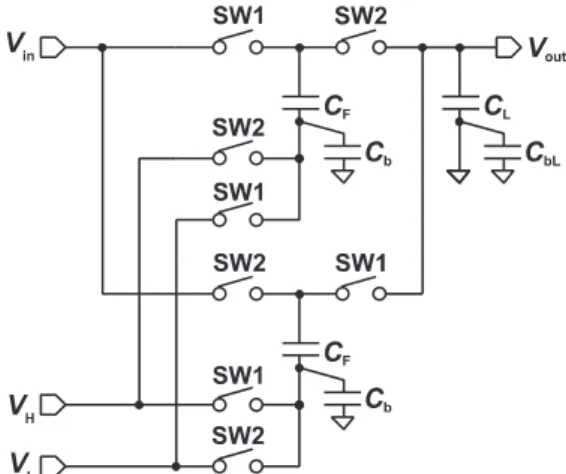
Figure 2 (b) shows a schematic of a modified SC VBC. The VBC consists of a flying metal-insulator-metal (MIM) capacitorCFand switches, which are driven by non- overlapping control clock signals. The VBC accepts two different voltages of VH andVL, which are different from Fig. 2 (a), and generates a higherVout with a lower number of stages. When SW1 and SW2 are ON and OFF, respec- tively,CFis charged withVin−VL. After that, when SW1 and SW2 toggle, the top potential ofCFcan be expressed as Vout=Vin+VH−VL, (1) because the bottom potential ofCFbecomesVH. This way, we can obtain a higher output voltage.
However, theVoutis disconnected fromCFwhen SW2 is OFF. This causes the output voltage to reduce and de- grades the power conversion efficiency (PCE). A comple- mentary circuit configuration is often adopted to cope with this problem[31]–[34]. Figure 3 (a) shows a schematic of the complementary circuit configuration including a load ca- pacitorCL. The complementary block is added to Fig. 2 (b).
Figure 3 (b) shows its circuit symbol.
To generate a higherVout, we can use multi-stage SC VBCs. As aforementioned, only one way can be utilized to obtain a higherVoutwhen we use simple VBCs [Fig. 2 (a)].
However, several ways are possible when we use modified VBCs [Fig. 2 (b)] because we can use intermediate output voltages at each stage asVH andVL. For example, three ways can be utilized to obtain 3×Vinas shown in Figs. 4 (a)–
4 (c). However, judging which topology is the best is quite difficult without performing SPICE simulations. Therefore, we need a design guideline to develop a highly efficient VBC.
Fig. 2 Schematics of (a) simple and (b) modified SC VBCs.
Fig. 3 (a) Complementary circuit configuration and (b) its circuit sym- bol.
Fig. 4 Topologies of 2-stage VBC (Vout=3×Vin).
3. Modeling for Multi-Stage SC VBC 3.1 Preliminaries
In this section, we discuss a method for modeling
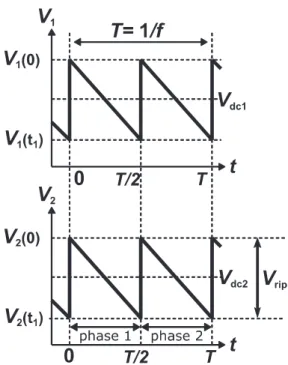
Fig. 5 Output waveforms of 1st (top) and 2nd stages (bottom).
multi-stage SC VBCs by taking Fig. 4 (a) as an example. In our modeling method, we suppose the following conditions.
1. All switches are ideal switches.
2. Parasitic capacitance can be ignored.
3. Currents flowing into the input terminals can be esti- mated from the output current.
4. The non-overlapping period of the clocks is extremely small.
Note that, with these conditions, output waveforms of each stage can be regarded as ideal sawtooth waves as shown in Fig. 5 when the output load current isIL, whereT (=1/f) is the clock period,f is the clock frequency,V1(0),V1(T/2), andVdc1 are the maximum, minimum, and average output voltages of the 1st stage, andV2(0),V2(T/2), andVdc2 are the maximum, minimum, and average output voltages of the 2nd stage. From Fig. 5, the average output voltages of each stage can be expressed as
Vdc1=V1(0)+V1(T/2)
2 , (2)
Vdc2=V2(0)+V2(T/2)
2 , (3)
and the ripple voltageVripat the output can be expressed as
Vrip=V2(0)−V2(T/2). (4)
Figure 6 shows currents flowing into the input and output terminals when SW1 and SW2 are OFF and ON, respec- tively. As shown in Fig. 6, when the load currentIL flows into the output, the same currentILflows fromVH. In addi- tion,ILalso flows fromVintoVL. Therefore, we obtain the following equation as
CF(Vin−VL)=ILT
2 . (5)
Fig. 6 Illustration of current flows.
Fig. 7 Equivalent topology of Fig. 4 (a) considering load current.
As depicted in Figs. 4 (a)–4 (c), we can estimate currents flowing into each terminal.
3.2 Equivalent Model of SC VBCs
Figure 7 shows an equivalent topology of Fig. 4 (a) consider- ing load current. We can divide the circuit into two circuits by using each output current and output voltage of the 1st stage as current and voltage sources as shown on the bottom in Fig. 7. By dividing a circuit into each stage, we can derive the output impedance.
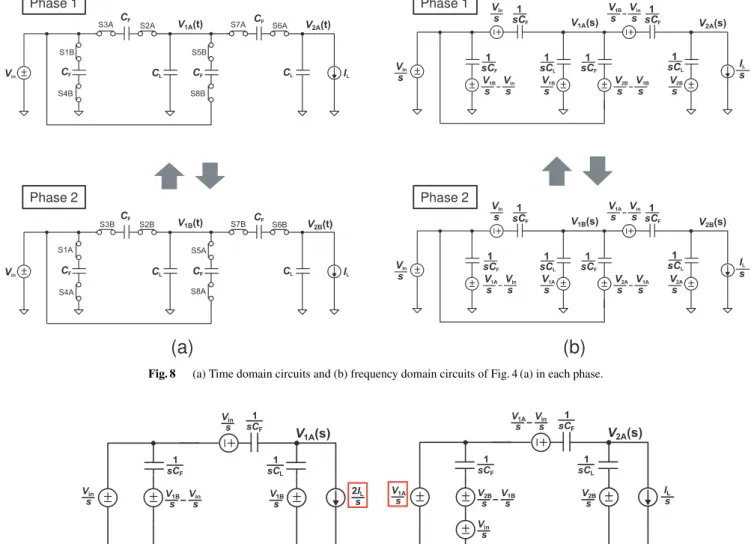
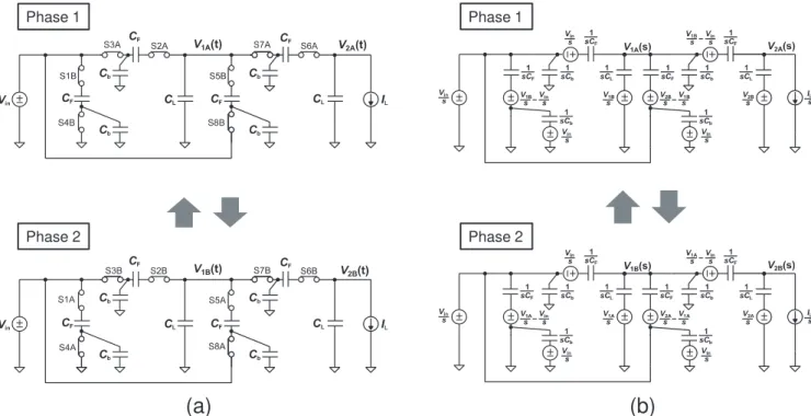
Figure 8 (a) shows time domain circuits in each phase.
The configuration in both phases are almost the same, except for ON switches (e.g., S1B is ON in phase 1, while S1A is ON in phase 2) because the SC VBC utilizes the comple- mentary circuit configuration. From Fig. 8 (a), we can re- draw frequency domain circuits as shown in Fig. 8 (b). Ini- tial voltages for the capacitors are expressed by the voltage sources, and their voltages are determined by the voltages at the end of each phase. We analyze phase 1 in the frequency domain because the VBC alternately operates in phase 1 and phase 2.
Figures 9 (a) and 9 (b) show the frequency domain cir- cuits of the 1st and 2nd stages, respectively. The output volt- age of the 1st stage can be solved using Kirchhoff’s current law (KCL) because the output current of the 1st stage is 2IL
as depicted in Fig. 4 (a). From the KCL for nodeV1A(s), we
HIROSE and NAKAZAWA: DESIGN OF SC VBC FOR LOW-VOLTAGE AND LOW-POWER ENERGY HARVESTING
449
Fig. 8 (a) Time domain circuits and (b) frequency domain circuits of Fig. 4 (a) in each phase.
Fig. 9 Frequency domain circuits of Fig. 4 (a): (a) 1st and (b) 2nd stage circuits.
can obtain the following equation:
V1A(s)−(Vsin+Vsin) 1/sCF +2IL
s +V1A(s)−V1B(Ts/2)
1/sCL =0. (6) Therefore,V1A(s) is expressed as
V1A(s)=α1
2Vin
s +α2
V1B(T/2)
s − 2IL
s2(CF+CL), (7) whereα1 =CF/(CF+CL) andα2 =CL/(CF+CL). From Eq. (7), we obtain the time domain voltageV1A(t) as
V1A(t)=α12Vin+α2V1B(T/2)− 2IL CF+CL
t. (8) Att=T/2, Eq. (8) can be expressed by
V1A(T/2)=2Vin−2IL
CF
T
2, (9)
becauseV1B(T/2) is equal toV1A(T/2) due to the symmetri- cal VBC’s operation. From the aforementioned analysis, we obtain the output voltage of the 1st stage, thereby enabling
us to analyze the 2nd stage using Eq. (9).
From the KCL for nodeV2A(s), we obtain the following equation:
V2A(s)−2V
1A
s −Vsin 1/sCF +IL
s+V2A(s)−V2B(Ts/2)
1/sCL =0. (10) Therefore,V2A(s) is expressed as
V2A(s)=α1
2V1A
s −Vin
s
+α2
V2B(T/2)
s − IL
s2(CF+CL). (11) From Eq. (11), we obtain the time domain voltageV2A(t) as
V2A(t)=α1(2V1A(T/2)−Vin)+α2V2B(T/2)− IL
CF+CLt.(12) Att=T/2, Eq. (12) can be expressed by
V2A(T/2)=3Vin−5IL CF
T
2, (13)
becauseV2B(T/2) is equal toV2A(T/2).
Fig. 10 Equivalent circuit model of Fig. 4 (a).
Table 2 Output impedance of each topology (2-stage VBC) 2-stage VBC (Vout=3Vin) Output impedance
Fig. 4 (a) 4f C9CF+10CL
F(CF+CL)
Fig. 4 (b) 4f C3CF+4CL
F(CF+CL)
Fig. 4 (c) 4f C3CF+4CL
F(CF+CL)
From Eqs. (3), (12), and (13), the average output volt- ageVdc2is given by
Vdc2=3Vin− 9CF+10CL
4f CF(CF+CL)IL. (14) From Eq. (14), we can derive an equivalent circuit model of Fig. 4 (a) as shown in Fig. 10. The model consists of a volt- age controlled voltage source, output impedance, and load current. The second term of Eq. (14) stands for the conduc- tion loss of the VBC, and, thus, we can model the perfor- mance of the multi-stage VBC.
Table 2 summarizes the calculated output impedance of each topology [Figs. 4 (a)–4 (c)]. As can be seen, the output impedance of Fig. 4 (a) is the largest, while those of Figs. 4 (b) and 4 (c) are the smallest and the same. This means that the circuit topology shown in Fig. 4 (a) is inap- propriate due to the large output impedance. In addition, we can find that the two input terminals ofVin andVHof the stage are exchangeable because the output impedances of Figs. 4 (b) and 4 (c) are the same.
3.3 Modeling with Parasitic Capacitance
In Sect. 3.2, we ignore the parasitic capacitance of the VBC to simplify the analysis. However, we must consider para- sitic capacitance to develop an accurate model. Figure 11 shows a modified schematic of Fig. 3 (a) with bottom-plate parasitic capacitancesCbandCbL. The parasitic capacitance can be expressed asCb =kCFandCbL = kCL, wherekis the process dependent parasitic capacitance’s parameter.
3.3.1 Output Voltage
Figure 12 shows time and frequency domain circuits of in- cluding bottom plate parasitic capacitance. We ignoreCbL
Fig. 11 Schematic of complementary VBC with bottom plate parasitic capacitance.
because the bottom plate voltage ofCLis kept at 0 V. With the same procedure as discussed in Sect. 3.2, the average output voltage of the 2-stage VBC is given by
Vdc2=(3−4k+k2)Vin−(9−4k)CF+(10−4k)CL
4f CF(CF+CL) IL. (15) Compared with Eq. (14), we find that parasitic capaci- tance reduces the maximum output voltage and its output impedance (the details of the derivation are discussed in Appendix).
3.3.2 Output Impedance and Ripple Voltage with Area Constraint
Each stage of the VBC has twoCFs and oneCL, and, thus, the total capacitanceCtotalper stage is 2CF+CL. The output impedanceZoutand ripple voltageVripcan be expressed by
Zout =(2β+1)((9−4k)β+(10−4k))
4β(β+1)f Ctotal , (16)
Vrip= IL
2f(CF+CL) = (2β+1)IL
2(β+1)f Ctotal, (17) whereβis the ratio ofCFandCL(i.e.,β=CF/CL). From Eqs. (16) and (17),Zoutdecreases andVripincreases asβin- creases. Therefore, we have to pay attention to the trade-off between the output impedance and ripple voltage.
3.3.3 Power Conversion Efficiency (PCE)
We can derive the PCE η using our model, which is ex- pressed as
η=Pout
Pin = Pout
Pout+Plossr+Plossb, (18) wherePinandPoutare the input and output power, andPlossr
andPlossbare the impedance loss and bottom-plate parasitic loss, respectively. From Eqs. (15) and (16), Pout andPlossr
are expressed as
Pout=Vdc2IL, (19)
HIROSE and NAKAZAWA: DESIGN OF SC VBC FOR LOW-VOLTAGE AND LOW-POWER ENERGY HARVESTING
451
Fig. 12 (a) Time domain circuits and (b) frequency domain circuits of Fig. 11 in each phase with bottom plate parasitic capacitance.
Plossr=ZoutIL2. (20)
Plossb can be obtained as follows. From Fig. 11, when SW1 or SW2 are ON,Cb(=kCF) is charged withVH. After that, when SWs toggle, the charge is discharged toVL. Therefore, Plossbcan be expressed as
Plossb= f kCFVin2 +f kCF(V1A(T/2)2−Vin2), (21) where the first and second terms are the loss in the first and second stages, respectively. Therefore, from Eqs. (18), (19), (20), (21), and (A·4) (see Appendix), the PCE can be ex- pressed as
η= ((3−4k+k2)Vin−(9−4k)C4f CFF(C+(10−4k)CF+CL) LIL)IL
(3−8k+3k2)VinIL+(2−k)2f kCFVin2+CkIF2Lf. (22) From Eq. (22), we find that the maximum PCE will be de- termined by not only the load currentIL but also the clock frequency f.
4. Results
4.1 Simulation Results
We evaluated the accuracy of our model by using SPICE with a set of 65-nm standard CMOS process parameters.
We designed 3-stage VBCs that generate 6×Vin. Figure 13 shows the circuit topologies we evaluated. Four topolo- gies are possible. Table 3 summarizes the calculated output impedance of each topology. From Table 3, we can estimate that Fig. 13 (a) has the smallest output impedance.
Fig. 13 Four possible topologies of 3-stage VBC (Vout=6×Vin).
In the following simulations, the input voltage Vin, switching frequency f, process dependent parasitic capac- itance’s parameterk, and on- and off-resistance of the ideal switches were set to 120 mV, 20 kHz, 0.005, 5Ω, and 1 TΩ, respectively. The voltage swing of the non-overlapping clock signal for MOS switches was set to 1.0 V for a fair performance comparison of the different topologies. We set
Ctotal(=2CF+CL) to 150 pF and investigated three different capacitance conditions: (CF,CL)=(20, 110 pF), (50, 50 pF), and (70, 10 pF).
Figures 14, 15, 16, and Table 4 show and summarize the comparison results. The results revealed that the output impedance of Fig. 13 (a) had the smallest output impedance as expected. Therefore, we found that Fig. 13 (a) was the most suitable configuration. Figure 14 shows the output voltage as a function of load current when we used ideal switches. We compared the simulated results with the cal- culated results, which were obtained using our proposed model. As shown in Fig. 14, the simulated and calculated results were almost the same in all cases, demonstrating that our proposed model could estimate the output impedance
Table 3 Output impedance of each topology (3-stage VBC) 3-stage VBC Output impedance
Fig. 13 (a) (4(2−k)2+4f C1)CF+(4(2−k)2+2)CL
F(CF+CL)
Fig. 13 (b) (2(1−k)(10−k)+1)CF+(2(1−k)(10−k)+2)CL 4f CF(CF+CL)
Fig. 13 (c) (2(2−k)(8−k)−4f C5)CF+(2(2−k)(8−k)−4)CL
F(CF+CL)
Fig. 13 (d) (2(2−k)(10−4k)+4f C1)CF+(2(2−k)(10−4k)+2)CL
F(CF+CL)
Fig. 14 Output voltage of VBC using ideal switches as function of load current.Ctotal(=2CF+CL) was set to 150 pF. Capacitances (CF,CL) were set to (a) (20, 110 pF), (b) (50, 50 pF), and (c) (70, 10 pF).
Fig. 15 Output voltage of VBC using MOS switches (L=60 nm) as function of load current. Ctotal
(=2CF+CL) was set to 150 pF. Capacitances (CF,CL) were set to (a) (20, 110 pF), (b) (50, 50 pF), and (c) (70, 10 pF).
of the multi-stage VBC accurately. We also found that a largerCFwidens the load current range. Figure 15 shows the output voltage as a function of load current when we used short-channel MOS switches. The channel length was set to 60 nm. The simulated output voltage slightly decreased as a whole, compared with the calculated results. In addi- tion, as can be seen in Fig. 15, the output impedances of the VBCs slightly decreased. This was because we used non- ideal MOS switches. We set theroffs of the ideal switches to 1 TΩ. However, theroffs of the MOS switches were less than the ideal ones. The MOS switches could not be suffi- ciently turned off. Therefore, the output voltages and out- put impedances decreased. Figure 16 shows the output volt- age as a function of load current when we use long-channel MOS switches. The channel length was set to 200 nm.
As channel length Lincreases, rons androffs increase[35].
Therefore, the output voltage was close to the calculated results.
We investigated the output impedance and ripple volt- age of Fig. 13 (a). We set Ctotal (= 2CF +CL) and load current IL to 150 pF and 20 nA, respectively. Figure 17 shows the simulated and calculated output impedance as a function of CF/CL. The output impedance decreased as CF/CL increased. The simulated output impedance showed good agreement with the calculated results. Figure 18 shows
HIROSE and NAKAZAWA: DESIGN OF SC VBC FOR LOW-VOLTAGE AND LOW-POWER ENERGY HARVESTING
453
Fig. 16 Output voltage of VBC using MOS switches (L=200 nm) as function of load current.Ctotal
(=2CF+CL) was set to 150 pF. Capacitances (CF,CL) were set to (a) (20, 110 pF), (b) (50, 50 pF), and (c) (70, 10 pF).
Table 4 Comparison of output impedance Output impedance [MΩ]
Topology (CF,CL)=(20, 110 pF) (CF,CL)=(50, 50 pF) (CF,CL)=(70, 10 pF)
Calc. Sim. Sim. Sim.
Calc. Sim. Sim. Sim.
Calc. Sim. Sim. Sim.
(ideal) (L=60nm) (L=200nm) (ideal) (L=60nm) (L=200nm) (ideal) (L=60nm) (L=200nm)
Fig. 13 (a) 11.1 11.2 10.8 11.0 4.36 4.39 4.34 4.33 3.04 3.13 3.10 3.01
Fig. 13 (b) 13.6 13.7 13.3 13.5 5.35 5.39 5.34 5.33 3.75 3.85 3.82 3.73
Fig. 13 (c) 17.3 17.6 17.1 16.9 6.85 6.84 6.82 6.78 4.83 4.86 4.85 4.72
Fig. 13 (d) 26.0 25.6 24.1 25.1 10.3 10.1 9.91 10.0 7.31 7.24 7.09 7.09
Fig. 17 Output impedance as function ofCF/CL.
the simulated and calculated ripple voltage as a function of CF/CL. The ripple voltage increased asCF/CL increased.
However, the simulated results increased more than the cal- culated results. This was because of the non-overlapping period of the clock generator. TheCFs were disconnected from theCLduring the non-overlapping period. In this situ- ation, the ripple voltage was determined by not only Eq. (17) but alsoCL,IL, and non-overlapping period. The simulated ripple voltage increased becauseCLdecreased asCF/CLin- creased. From Figs. 17 and 18, we have to pay attention to the trade-offbetween the load range and ripple voltage.
Fig. 18 Ripple voltage as function ofCF/CL.
We evaluated the PCE of Fig. 13 (a). We setCF,CL, andIL to 50, 50 pF, 20 nA, respectively. Figure 19 shows PCE as a function of frequency. Compared with the cal- culated results, the simulated results using ideal and MOS switches were lower than the calculated results. This was because of the on- and off-resistance of the MOS switches.
In our calculated model, we ignored ron and roff. How- ever, in a higher frequency range, the power loss inronand roff increased, and the PCE degraded. We also found that there was a suitable clock frequency that maximizes the PCE when the load current was fixed.
Fig. 19 PCE as function of clock frequency.
Fig. 20 Chip micrograph.
4.2 Experimental Results
A prototype SC VBC using Fig. 13 (a) was fabricated with 65-nm CMOS process technology. The load capacitance was set to 30 pF. The input voltage was set to 0.5 V, which was supplied by the voltage source. Figure 20 shows the chip micrograph (area: 0.46 mm2) including the SC VBC and other peripheral circuits.
Figures 21 and 22 show the measured output voltage and efficiency as a function of load current. The load range that could generate a voltage higher than 1.2 V was 0 to 1.46 μA. The maximum PCE was 68.3% at IL =0.4 μA.
The power dissipation of the VBC was 126 nW.
Figure 23 shows the measured voltage conversion ratio (VCR) as a function of the input voltage when unloaded. We defined the minimum supply voltage as the input voltage at which the VCR was higher than 5.5. From Fig. 23, the minimum input voltage was 220 mV.
To demonstrate the feasibility of our energy harvesting system, we used a small-size photovoltaic (PV) cell as an en- ergy harvester. Figure 24 shows a micrograph of the silicon PV cell we used and its measured characteristics. The size
Fig. 21 Measured output voltage as function of load current.
Fig. 22 Measured PCE as function of load current.
Fig. 23 Measured voltage conversion ratio as function ofVin.
of the PV cell was 2.5×2.5 mm. The open circuit voltage and the maximum output power of the PV cell were 0.33 V and 400 nW, respectively, at a room light intensity of 850 lx.
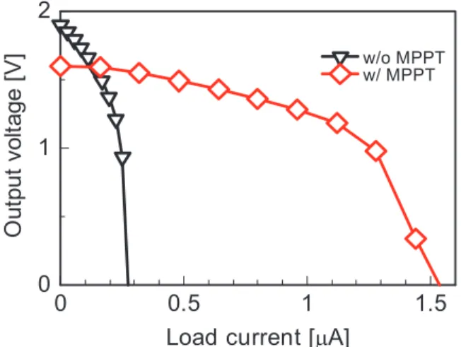
Figure 25 shows the measured output voltage as a func- tion of load current, with and without a maximum power point tracking (MPPT) control circuit. The MPPT control circuit reported in [17], [20] was adopted in this design
HIROSE and NAKAZAWA: DESIGN OF SC VBC FOR LOW-VOLTAGE AND LOW-POWER ENERGY HARVESTING
455
Fig. 24 On chip PV cell: (a) chip micrograph and (b) measured charac- teristics.
Fig. 25 Measured output voltage as function of load current.
(details of the MPPT are not discussed in this paper). As can be seen, the load range increased significantly thanks to the MPPT circuit. The output voltage with the MPPT circuit was lower than that without the MPPT circuit in a light load- current region. This was because the output voltage of the PV cell decreased to 0.26 V due to the current dissipation of the MPPT circuit.
5. Conclusion
This paper presented an analytical model of a multi-stage SC VBC for low-voltage and low-power energy harvest- ing. In our proposed method, we focus on currents flowing into input and output terminals of each stage and model the VBCs by using switching frequency f, charge transfer ca- pacitanceCF, load capacitanceCL, and process dependent parasitic capacitance’s parameterk. A comparison between simulated and calculated results showed that our model can accurately estimate the output impedance of the VBC. By using our model, we can achieve a highly efficient VBC. A prototype SC VBC and energy harvesting using the SC VBC were also developed to show the effectiveness and feasibility of our proposed design guideline.
Acknowledgments
This work was based on results obtained from a project
commissioned by the New Energy and Industrial Technol- ogy Development Organization (NEDO) of Japan, and it was conducted through a dedicated licensing program pro- vided by the VLSI Design and Education Center (VDEC) at the University of Tokyo with the cooperation of Cadence Design Systems, Inc. and Mentor, a Siemens business.
This work was also partially supported by JSPS KAKENHI Grant Number JP19K11875 and the Canon Foundation.
References
[1] L.D. Xu, W. He, and S. Li, “Internet of things in industries: A sur- vey,” IEEE Trans. Ind. Informat., vol.10, no.4, pp.2233–2243, 2014.
[2] D. Blaauw, D. Sylvester, P. Dutta, Y. Lee, I. Lee, S. Bang, Y. Kim, G.
Kim, P. Pannuto, Y.-S. Kuo, D. Yoon, W. Jung, Z. Foo, Y.-P. Chen, S. Oh, S. Jeong, and M. Choi, “IoT design space challenges: Cir- cuits and systems,” Symp. VLSI Technol. Dig. Tech. Papers, pp.1–2, 2014.
[3] V. Raghunathan and P.H. Chou, “Design and power management of energy harvesting embedded systems,” Proc. Int. Symp. Low Power Electron. Design (ISLPED), pp.369–374, 2006.
[4] A.P. Chandrakasan, D.C. Daly, J. Kwong, and Y.K. Ramadass, “Next generation micro-power systems,” Symp. VLSI Circuits Dig. Tech.
Papers, pp.2–5, 2008.
[5] T. Hirose, R. Yoshimura, T. Ido, T. Matsuoka, and K. Taniguchi,
“Watch-dog circuit for quality guarantee with subthreshold MOSFET current,” IEICE Trans. Electron., vol.E87-C, no.11, pp.1910–1914, 2004.
[6] K. Ueno, T. Hirose, T. Asai, and Y. Amemiya, “CMOS smart sen- sor for monitoring the quality of perishables,” IEEE J. Solid-State Circuits, vol.42, no.4, pp.798–803, 2007.
[7] K. Ueno, T. Hirose, T. Asai, and Y. Amemiya, “A CMOS watch- dog sensor for certifying the quality of various perishables with a wider activation energy,” IEICE Trans. Fundamentals, vol.E89-A, no.4, pp.902–907, 2006.
[8] H. Asano, T. Hirose, K. Tsubaki, T. Miyoshi, T. Ozaki, N. Kuroki, and M. Numa, “A 1.66-nW/kHz, 32.7-kHz, 99.5ppm/◦C, fully in- tegrated current-mode RC oscillator for real-time clock applica- tions with PVT stability,” Proc. Eur. Solid-State Circuits Conf.
(ESSCIRC), pp.149–152, 2016.
[9] R. Matsuzuka, T. Terada, K. Matsumoto, M. Kitamura, and T.
Hirose, “A 42 mV startup ring oscillator using gain-enhanced self- bias inverters for extremely low voltage energy harvesting,” Jpn. J.
Appl. Phys., vol.59, 0SGGL01, 2020.
[10] M. Nishi, Y. Nakazawa, K. Matsumoto, N. Kuroki, M. Numa, R.
Matsuzuka, O. Maida, D. Kanemoto, and T. Hirose, “Sub-0.1V in- put, low-voltage CMOS driver circuit for multi-stage switched ca- pacitor voltage boost converter,” Proc. Int. Conf. Electron. Circuits Syst. (ICECS), pp.530–533, 2019.
[11] S. Kanzaki, T. Hirose, H. Asano, Y. Nakazawa, N. Kuroki, and M. Numa, “Switched-capacitor voltage buck converter with step- down-ratio and clock-frequency controllers for ultra-low-power IoT devices,” Proc. Int. Conf. Electron. Circuits Syst. (ICECS), pp.209–212, 2018.
[12] K. Matsumoto, T. Hirose, H. Asano, Y. Tsuji, Y. Nakazawa, N.
Kuroki, and M. Numa, “An ultra-low power active diode using a hys- teresis common gate comparator for low-voltage and low-power en- ergy harvesting systems,” 2018 IFIP/IEEE International Conference on Very Large Scale Integration (VLSI-SoC), pp.196–200, 2018.
[13] T. Ozaki, T. Hirose, H. Asano, N. Kuroki, and M. Numa, “Ul- tralow-quiescent-current and wide-load-range low-dropout linear regulator with self-biasing technique for micropower battery man- agement,” Jpn. J. Appl. Phys., vol.56, 04CF11, 2017.
[14] T. Sato, T. Hirose, H. Asano, N. Kuroki, and M. Numa,
“An ultra-low-power supercapacitor voltage monitoring system for
low-voltage energy harvesting,” Proc. Int. Conf. Electron. Circuits Syst. (ICECS), pp.498–501, 2017.
[15] T. Ozaki, T. Hirose, H. Asano, N. Kuroki, and M. Numa,
“A 0.38-μW stand-by power, 50-nA-to-1-mA load current range DC-DC converter with self-biased linear regulator for ultra-low power battery management,” Proc. Asian Solid-State Circuits Conf.
(A-SSCC), pp.225–228, 2016.
[16] Y. Osaki, T. Hirose, N. Kuroki, and M. Numa, “1.2-V supply, 100-nW, 1.09-V bandgap and 0.7-V supply, 52.5-nW, 0.55-V sub- bandgap reference circuits for nano-watt CMOS LSIs,” IEEE J.
Solid-State Circuits, vol.48, no.6, pp.512–518, 2014.
[17] T. Ozaki, T. Hirose, T. Nagai, K. Tsubaki, N. Kuroki, and M. Numa,
“A highly efficient switched-capacitor voltage boost converter with nano-watt MPPT controller for low-voltage energy harvesting,”
IEICE Trans. Fundamentals, vol.E99-A, no.12, pp.2491–2499, 2016.
[18] T. Ozaki, T. Hirose, H. Asano, N. Kuroki, and M. Numa, “Fully- integrated high-conversion-ratio dual-output voltage boost converter with MPPT for low-voltage energy harvesting,” IEEE J. Solid-State Circuits, vol.51, no.10, pp.2398–2407, 2016.
[19] Y. Tsuji, T. Hirose, T. Ozaki, H. Asano, N. Kuroki, and M. Numa,
“A 0.1-0.6 V input range voltage boost converter with low-leakage driver for low-voltage energy harvesting,” Proc. Int. Conf. Electron.
Circuits Syst. (ICECS), pp.502–505, 2017.
[20] T. Ozaki, T. Hirose, T. Nagai, K. Tsubaki, N. Kuroki, and M. Numa,
“A 0.21-V input, 73.6% efficiency, fully integrated voltage boost converter with maximum power point tracking for low-voltage en- ergy harvesters,” Proc. Eur. Solid-State Circuits Conf. (ESSCIRC), pp.255–258, 2014.
[21] P.-H. Chen, K. Ishida, X. Zhang, Y. Okuma, Y. Ryu, M. Takamiya, and T. Sakurai, “A 120-mV input, fully integrated dual-mode charge pump in 65-nm CMOS for thermoelectric energy harvester,”
Proc. Asia South Pacific Design Automation Conf. (ASP-DAC), pp.469–470, 2012.
[22] Y.K. Ramadass and A.P. Chandrakasan, “A battery-less thermoelec- tric energy harvesting interface circuit with 35 mv startup voltage,”
IEEE J. Solid-State Circuits, vol.46, no.1, pp.333–341, 2011.
[23] M.-D. Ker, S.-L. Chen, and C.-S. Tsai, “Design of charge pump circuit with consideration of gate-oxide reliability in low-volt- age CMOS processes,” IEEE J. Solid-State Circuits, vol.41, no.5, pp.1100–1107, 2006.
[24] Y.-C. Shih and B.P. Otis, “An inductorless DC-DC converter for energy harvesting with a 1.2μw bandgap-referenced output con- troller,” IEEE Trans. Circuits Syst. II, Exp. Briefs, vol.58, no.12, pp.832–836, 2011.
[25] H. Lee and P.K.T. Mok, “An SC voltage doubler with pseudo-contin- uous output regulation using a three-stage switchable opamp,” IEEE J. Solid-State Circuits, vol.42, no.6, pp.1216–1229, 2007.
[26] Y.-H. Chang and Y.-C. Chen, “Multistage multiphase switched-ca- pacitor DC-DC converter with variable-phase and PWM control,”
Int. J. Circuit Theory Appl., vol.40, no.8, pp.835–857, 2012.
[27] C.M. Wildrick, F.C. Lee, B.H. Cho, and B. Choi, “A method of defining the load impedance specification for a stable dis- tributed power system,” IEEE Trans. Power Electron., vol.10, no.3, pp.280–285, 1995.
[28] P. Xiao, G. Venayagamoorthy, and K. Corzine, “A novel impedance measurement technique for power electronic systems,” Proc. Power Electron. Specialists Conf. (PESC), pp.955–960, 2007.
[29] J.F. Dickson, “On-chip high-voltage generation in MNOS integrated circuits using an improved voltage multiplier technique,” IEEE J.
Solid-State Circuits, vol.11, no.3, pp.374–378, 1976.
[30] T. Tanzawa, “A comprehensive optimization methodology for de- signing charge pump voltage multipliers,” Proc. Int. Symp. Circuits Syst. (ISCAS), pp.1358–1361, 2015.
[31] Y. Nakazawa, T. Hirose, T. Ozaki, Y. Tsuji, S. Kanzaki, H. Asano, N. Kuroki, and M. Numa, “Analytical study of multi-stage switched- capacitor voltage boost converter for ultra-low voltage energy
harvesting,” Proc. Int. Symp. Circuits Syst., pp.1–5, 2018.
[32] T. Hirose, T. Asai, and Y. Amemiya, “Power-supply circuits for ul- tralow-power subthreshold MOS-LSIs,” IEICE Electron. Express, vol.3, no.22, pp.464–468, 2006.
[33] Y. Kojima, T. Hirose, K. Tsubaki, T. Ozaki, H. Asano, N. Kuroki, and M. Numa, “A fully on-chip three-terminal switched-capacitor DC-DC converter for low-voltage CMOS LSIs,” Jpn. J. Appl. Phys., vol.55, 04EF09, 2016.
[34] H. Asano, T. Hirose, Y. Kojima, N. Kuroki, and M. Numa, “A fully integrated, wide-load-range, high-power-conversion-efficiency switched capacitor DC-DC converter with adaptive bias comparator for ultra-low-power power management integrated circuit,” Jpn. J.
Appl. Phys., vol.57, 04FF03, 2018.
[35] A.K. Ong, V.I. Prodanov, and M. Tarsia, “A method for reducing the variation in “on” resistance of a MOS sampling switch,” Proc. Int.
Symp. Circuits Syst. (ISCAS), pp.437–440, 2000.
Appendix:
Equation (15) can be obtained in the same manner as deriv- ing Eq. (14). Details are as follows.
From the KCL for nodeV1A(s) in Fig. 12 (b), we obtain the following equation:
V1A(s)−(Vsin +Vsin) 1/sCF +2IL
s +V1A(s)−V1B(Ts/2)
1/sCL +
Vin
s
1/skCF =0. (A·1) Therefore,V1A(s) is expressed as
V1A(s)=α1
(2−k)Vin
s +α2
V1B(T/2)
s − 2IL
s2(CF+CL), (A·2) whereα1 =CF/(CF+CL) andα2 =CL/(CF+CL). From Eq. (A·2), we obtain the time domain voltageV1A(t) as
V1A(t)=α1(2−k)Vin+α2V1B(T/2)− 2IL
CF+CLt. (A·3) Att=T/2, Eq. (A·3) can be expressed by
V1A(T/2)=(2−k)Vin−2IL
CF
T
2. (A·4)
This is because V1B(T/2) is equal to V1A(T/2) due to the symmetrical VBC’s operation. From the aforemen- tioned analysis, we obtain the output voltage of the 1st stage, thereby enabling us to analyze the 2nd stage using Eq. (A·4).
From the KCL for nodeV2A(s), we obtain the following equation:
V2A(s)−2V
1A
s −Vsin 1/sCF +IL
s +V2A(s)−V2B(Ts/2)
1/sCL
+
V1A(T/2) s
1/skCF
=0. (A·5) Therefore,V2A(s) is expressed as
V2A(s) = α1
(2−k)V1A s −Vin
s
HIROSE and NAKAZAWA: DESIGN OF SC VBC FOR LOW-VOLTAGE AND LOW-POWER ENERGY HARVESTING
457
+α2
V2B(T/2)
s − IL
s2(CF+CL). (A·6) From Eq. (A·6), we obtain the time domain voltageV2A(t) as
V2A(t)= α1((2−k)V1A(T/2)−Vin) +α2V2B(T/2)− IL
CF+CLt. (A·7) Att=T/2, Eq. (A·7) can be expressed by
V2A(T/2)=(3−4k+k2)Vin−(5−2k)IL
CF T
2. (A·8) This is becauseV2B(T/2) is equal toV2A(T/2).
From Eqs. (3), (A·7), and (A·8), the average output voltageVdc2is given by
Vdc2=(3−4k+k2)Vin−(9−4k)CF+(10−4k)CL
4f CF(CF+CL) IL. (A·9)
Tetsuya Hirose received B.S., M.S., and Ph.D. degrees from Osaka University, Osaka, Japan, in 2000, 2002, and 2005, respectively.
From 2004 to 2008, he was a Research Asso- ciate with the Department of Electrical Engi- neering, Hokkaido University, Sapporo, Japan.
From 2008 to 2019, he was an Associate Profes- sor with the Department of Electrical and Elec- tronics Engineering, Kobe University, Kobe, Japan. Since 2019, he has been currently a Pro- fessor with the Division of Electrical, Electronic and Information Engineering, Graduate School of Engineering, Osaka Uni- versity, Suita, Japan. He has authored or co-authored over 200 journal and conference papers. His current research interests are extremely low-voltage and low-power analog/digital mixed-signal integrated circuit design and smart sensor systems. Dr. Hirose is a member of the Institute of Electron- ics, Information and Communication Engineers (IEICE), the Japan Society of Applied Physics (JSAP), and the Institute of Electrical and Electronics Engineers (IEEE). He served as a Technical Program Committee Member of the International Conference on Solid-State Devices and Materials from 2010 to 2013, and he has been a Technical Program Committee Member of the Asian Solid-State Circuits Conference since 2011, an Associate Editor for the IEICE Electronics Express from 2012 to 2015, the Chapter Secre- tary of the IEEE SSCS Kansai Chapter from 2015 to 2016, and a Guest Associate Editor for the special issues of IEICE Transactions on Funda- mentals and Electronics since 2010.
Yuichiro Nakazawa received the B.S.
and M.S. degrees from Kobe University, Kobe, Japan, in 2017 and 2019, respectively. In 2019, he joined Richo Electronic Devices Co., Ltd., Japan.