INVITED PAPER
Joint Special Section on Opto-electronics and Communications for Future Optical NetworkNumerical Study on Fabrication Tolerance of Half-Ridge InP Polarization Converters
Masaru ZAITSU†a),Student Member, Takuo TANEMURA†,Member,andYoshiaki NAKANO†,Fellow
SUMMARY Integrated InP polarization converters based on half-ridge structure are studied numerically. We demonstrate that the fabrication tol- erance of the half-ridge structure can be extended significantly by intro- ducing a slope at the ridge side and optimizing the thickness of the residual InGaAsP layer. High polarization conversion over 90% is achieved with the broad range of the waveguide width from 705 to 915 nm, correspond- ing to a factor-of-two or larger improvement in the fabrication tolerance compared with that of the conventional polarization converters. Finally we present a simple fabrication procedure of this newly proposed structure, where the thickness of the residual InGaAsP layer is controlled precisely by using a thin etch-stop layer.
key words: Polarization converters, fabrication tolerances, monolithic in- tegration, polarization-multiplexing, photonic integrated circuits
1. Introduction
The number of optical components and the complexity in the optical communication systems have been increasing for adapting to the expansion of the channel capacity in the wavelength division multiplexing (WDM) and more ad- vanced coherent modulation formats. Polarization division multiplexing (PDM) has been recently applied in the opti- cal transmission links as a powerful technique to double the spectral efficiency. Meanwhile, photonic integrated circuits (PICs) have been demonstrated to reduce the cost and size of such highly complicated optical transceivers. There has been a growing interest in realizing compact and low-cost PDM optical transceivers by using the PICs [1]–[4]. In or- der to manipulate the dual polarization states inside the PICs and realize fully integrated PDM-PICs, integrated polariza- tion converters (PCs) are essential.
Various types of PCs have been demonstrated to date;
those based on periodic loaded waveguides [5], micro- bended waveguides [6], adiabatic waveguides [7]–[10], and asymmetric waveguides [11]–[19]. The asymmetric PCs are suitable for monolithic integration with InP photonic de- vices as well as their short operating length and relatively small sensitivity against the deviation of the wavelength and the temperature. However, integration of the InP PCs with laser diodes (LDs) and other active components has been challenging. First, most asymmetric PCs are fabricated on
Manuscript received November 14, 2013.
Manuscript revised January 17, 2014.
†The authors are with the Department of Electrical Engineer- ing and Information Systems (EEIS), Graduate School of Engi- neering, The University of Tokyo, Hongo, Bunkyo-ku, Tokyo 113- 8656, Japan.
a) E-mail: [email protected] DOI: 10.1587/transele.E97.C.731
rib waveguide, while other components in InP-PICs usually have ridge structures. Such structural mismatch often leads to large coupling losses and requires relatively complicated fabrication procedures which may not suit the generic fab- rication technologies [20]. Another important issue is the strict fabrication tolerances of these types of PCs, where both the waveguide width and lithographic alignment have to be controlled within typically 100-nm accuracy. In this respect, a simple PC with a ridge-like waveguide structure having large fabrication tolerances is highly desired.
We have recently proposed and experimentally demon- strated a half-ridge InP/InGaAsP PC, which particularly suits the integration with LDs because of its ridge-like struc- ture and a simple self-aligned fabrication process [21], [22].
More than 96% polarization conversion has been experi- mentally obtained with the PC length of 150 µm and the wide wavelength range covering the entireC-band.
In this paper, we numerically study the efficiency and the fabrication tolerances of this InP half-ridge PC. We demonstrate that a residual InGaAsP layer with a slope at the ridge side plays a crucial role in extending the tolerance against the deviation of the waveguide width. A factor-of- two improvement in fabrication tolerance is obtained with the optimized design. In addition, we propose a novel design of the layerstack with a thin etch-stop layer for controlling the thickness of the residual InGaAsP layer precisely. We then propose a simple fabrication procedure for the newly proposed half-ridge PC with an improved design.
2. Device structure and numerical model
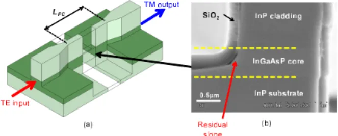
Figure 1 shows the structure of the InP half-ridge PC, hav- ing an asymmetric cross section: One side of the waveguide has a shallow ridge structure with a residual InGaAsP core layer and the other has a deeply-etched high-mesa structure.
Fig. 1 (a) Schematic of the integrated half-ridge PC, (b) Cross-section image of the fabricated PC [22].
Copyright c⃝2014 The Institute of Electronics, Information and Communication Engineers
Fig. 2 Polarization conversion inside asymmetric waveguides.
By optimizing the waveguide widthwand the residual core thicknessd (see Fig. 2), this asymmetric waveguide oper- ates as a birefringent medium with the principal axis ro- tated by±45◦. In such a case, as shown in Fig. 2, a hori- zontally polarized, transverse electric (TE) mode input light excites the two eigenmodes in the PC with an equal mag- nitude, which would recombine into a vertically polarized, transverse magnetic (TM) mode after propagating the half- beat length [Lπ =π/(β1−β2), whereβmis the propagation constant of modemin the half-ridge PC].
The eigenmodes in a given cross-sectional structure of the PC are calculated by using a full-vector finite difference method [23]. As a measure of the angle of equivalent princi- pal axes of the eigenmodes, we define the rotation parameter Rby
R≡
"
|Hx|2dxdy/"
Hy2dxdy (1) whereHxandHyare thex- andy-components of the mag- netic fields of the eigenmode, respectively. This parameter approximately expresses a rotation angleθof the principal axes of the eigenmodes in waveguides as
R≈|Hx|2
Hy2 =1/tan2θ. (2) The maximum conversion ratioCmax is approximately ex- pressed byRas
Cmax=sin22θ≈ 4R
(1+R)2. (3)
A net TE-to-TM conversion ratioC is expressed by using CmaxandLπas
C=Cmax·1 2
{ 1−cos
(π LπLPC
)}
(4) whereLPC is the length of the PC section. The TE-to-TM conversion ratio follows Eq. 4, a sinusoidal function ofLPC
as shown in Fig. 2.
In our previous demonstration [22], the fabricated de- vice had a residual slope at the ridge side of the InGaAsP core as shown in Fig. 1(b), which was due to a slight anisotropic etching during the Cl2/Ar dry-etching process.
In order to allow direct comparison with the actual devices,
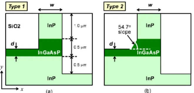
Fig. 3 Cross-section structure of the half-ridge PC: (a) Type 1 has a rect- angular ridge side. (b) Type 2 has a 54.7◦residual slope on the InGaAsP core which reflects the structure of the actual device shown in Fig. 1.
we assume two types of half-ridge PCs in our calculation.
They have different cross-sectional structures as shown in Fig. 3. Type 1 has a rectangular etching profile at the ridge side as designed initially [21]. On the other hand, Type 2 has a 54.7◦slope corresponding to (111) crystal plane of the InGaAsP, which reflects the actual fabricated device [22].
The eigenmodes in each structure are calculated for various values of the width of the PCwand the residual InGaAsP thicknessdat the ridge side. The thicknesses of the InP top cladding, the InGaAsP entire core, and the overetched depth of the InP bottom cladding are fixed to be 1.0µm, 0.50µm, and 0.50µm, respectively. The refractive indices of InP, In- GaAsP, and background (SiO2) are set to 3.17, 3.40, and 1.45, respectively. The wavelength is set to 1.55µm during the simulation.
3. Numerical results
Figures 4 and 5 show the calculatedCmaxandLπas a func- tion ofwanddfor Type 1 and Type 2, respectively. In both types, a conversion ratio of more than 99% is obtained by selecting w andd appropriately. We see from the figures that bothCmax andLπ become less sensitive towas we in- creasedfrom 0 to 0.30µm. This implies that the residual In- GaAsP layer at the ridge side has a crucial role of extending the tolerance against the fabrication error inw. We also see that the fabrication tolerances in bothwanddare larger for Type 2 compared with Type 1; the residual slope at the ridge side contributes to the increase in the tolerances. In the case of asymmetric PCs, triangular shape is the most ideal cross sectional structure to obtain efficient TE-to-TM conversion with short length [24]. The residual slope on the InGaAsP makes the light-confinement structure closer to the triangu- lar shape, and therefore the tolerances in Type 2 is enlarged compared with Type 1.
The fabrication tolerance of an actual PC with a fixed lengthLPC can be calculated by inserting the results plotted in Fig. 4 or 5 into Eq. 4. First, we selectwanddat which Cmaxapproaches 100%, and setLPC =Lπ. Under this fixed length ofLPC, the allowed range ofwanddcan be obtained from Eq. 4 and Fig. 4 or 5.
Figure 6 shows the calculated net conversion C for Type 1 and Type 2 as a function ofwatd=0.30µm.LPCis fixed to 200µm for Type 1 and 100µm for Type 2, which are
Fig. 4 Calculation result for Type 1 structure: (a) Maximum conversion ratioCmax, (b) Half-beat lengthLπas a function ofwandd.
Fig. 5 Calculation result for Type 2 structure: (a) Maximum conversion ratioCmax, (b) Half-beat lengthLπas a function ofwandd.
the optimized length to maximize the fabrication tolerance ofw. From Fig. 6, we see that a higher net conversion than 90% is obtained withw =810±105 nm for Type 2, while w =1000±50 nm for Type 1. We thus achieve factor-of- two improvement in the fabrication tolerance by using Type 2 over Type 1. Moreover, the half-beat length of Type 2 is also reduced to half than that of Type 1. We should note that this value of fabrication tolerance is larger than other types of asymmetric InP PCs [12], [15], and is readily achieved by the current fabrication technology.
4. Proposal of a width-tolerant PC using a novel layer- stack
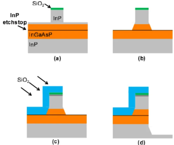
Figure 7 shows the proposed procedure to fabricate Type 2 PC. As we have demonstrated in the previous section, the precise control of the thickness of the residual InGaAsP layerd is crucial in achieving a high fabrication tolerance inw. To this end, we propose to introduce a few-nm-thick InP etch-stop layer at the middle of the InGaAsP core. Af- ter forming a ridge waveguide along [01¯1] direction by dry etching (a), we selectively wet-etch InGaAsP layer until the InP etch-stop layer, so that a precisely defined slope corre- sponding to the (111) plane is formed. Similar to the half- ridge fabrication procedure [22], SiO2is deposited from an angle, covering only one side of the ridge waveguide (c). Fi- nally, the Type 2 structure is obtained after the second dry- etching (d).
The etching depth of the InGaAsP can be precisely controlled with a nanometer-scale precision by using the
Fig. 6 Calculated net conversion ratioCas a function of converter width w, using Type 1 PC,LPC=200µm (dashed line), and Type 2 PC,LPC= 100µm (solid line).
Fig. 7 Fabrication procedure of Type 2 PC using an InP etch-stop layer at the middle of the InGaAsP core.
InP etch-stop layer, owing to the excellent selectivity of the chemical etching process such as H2SO4+H2O2+H2O sys- tem [25]. Consequently, we can precisely tune the value of d in Type 2 PC. Although there would be a slight undercut during the InGaAsP wet etching, this effect should be negli- gible or easily calibrated because the total etching depth in this case is 0.20 µm and the etching rate of (111) plane is much slower than (100) plane.
5. Conclusion
We have presented numerical analyses on the integrated InP/InGaAsP PCs based on the half-ridge structure. From the analyses of both the original design (Type 1) and the ac- tual fabricated structure (Type 2), we have revealed that the residual InGaAsP layer, as well as the slope at the ridge side plays an important role in extending the tolerances against fabrication errors. As an example case, we have demon- strated a high polarization conversion over 90% with a broad range of the waveguide width from 705 to 915 nm. Fi- nally, we proposed a simple fabrication procedure of this new type of PC, where a thin etch-stop layer was introduced to control the thickness of the residual InGaAsP layer pre- cisely. With the inherent compatibility with other active InP
Japan Society for the Promotion of Science (JSPS).
References
[1] M. Kato, P. Evans, S. Corzine, J. Gheorma, M. Fisher, M. Raburn, A. Dentai, R. Salvatore, I. Lyubomirsky, A. Nilsson, J. Rahn, R. Na- garajan, C. Tsai, B. Behnia, J. Stewart, D. Christini, M. Missey, A. Spannagel, D. Lambert, S. Agashe, P. Liu, D. Pavinski, M. Ref- fle, R. Schneider, M. Ziari, C. Joyner, F. Kish, and D. Welch,
“Transmitter PIC for 10-channel×40 Gb/s per channel polarization- multiplexed RZ-DQPSK modulation,” in proc. Optical Fiber Com- munication Conference (OFC2009), paper OThN2, San Diego, CA, USA, Mar. 2009.
[2] H. Yamazaki, T. Yamada, T. Goh, and A. Kaneko, “PDM-QPSK modulator with a hybrid configuration of silica PLCs and LiNbO3
phase modulators,” J. Lightw. Technol., vol. 29, no. 5, pp. 721–727, Mar. 2011.
[3] R. Nagarajan, J. Rahn, M. Kato, J. Pleumeekers, D. Lambert, V. Lal, H. S. Tsai, A. Nilsson, A. Dentai, M. Kuntz, R. Mal- endevich, J. Tang, J. Zhang, T. Butrie, M. Raburn, B. Little, W. Chen, G. Goldfarb, V. Dominic, B. Taylor, M. Reffle, F. Kish, and D. Welch, “10 channel, 45.6 Gb/s per channel, polarization- multiplexed DQPSK, InP receiver photonic integrated circuit,” J.
Lightw. Technol., vol. 29, no. 4, pp. 386–395, Feb. 2011.
[4] C.R. Doerr, N.K. Fontaine, and L.L. Buhl, “PDM-DQPSK silicon receiver with integrated monitor and minimum number of controls,”
Photon. Technol. Lett., vol. 24, no. 8, pp. 697–699, Apr. 2012.
[5] Y. Shani, R. Alferness, T. L. Koch, U. Koren, M. Oron, B. I. Miller, and M. G. Young, “Polarization rotation in asymmetric periodic loaded rib waveguides,” Appl. Phys. Lett., vol. 59, no. 11, pp. 1278–
1280, Sept. 1991.
[6] C. van Dam, L. H. Spiekman, F. P. G. M. van Ham, F. H. Groen, J. J. G. M. van der Tol, I. Moerman, W. W. Pascher, M. Hamacher, H. Heidrich, C. M. Weinert, and M.K. Smit, “Novel compact polar- ization convertors based on ultra short bends,” IEEE Photon. Tech- nol. Lett., vol. 8, no. 10, pp. 1346–1348, Oct. 1996.
[7] M. R. Watts and H. A. Haus, “Integrated mode-evolution-based po- larization rotators,” Opt. Lett., vol. 30, no. 2, pp. 138–140, Jan. 2005.
[8] T. Barwicz, M. R. Watts, M. A. Popovi´c, P. T. Rakich, L. Socci, F. X. Kärtner, E. P. Ippen, and H. I. Smith, “Polarization-transparent microphotonic devices in the strong confinement limit,” Nat. Pho- tonics, vol. 1, pp. 57–60, Jan. 2006.
[9] H. Fukuda, K. Yamada, T. Tsuchizawa, T. Watanabe, H. Shinojima, and S. Itabashi, “Polarization rotator based on silicon wire waveg- uides,” Opt. Express, vol. 16, no. 4, pp. 2628–2635, Feb. 2008.
[10] J. Zhang, T. Y. Liow, M. Yu, G. Q. Lo, and D.L. Kwong, “Silicon waveguide based TE mode converter,” Opt. Express, vol. 18, no. 24, pp. 25264–25270, Nov. 2010.
[11] J. Z. Huang, R. Scarmozzino, G. Nagy, M. J. Steel, and R. M. Os- good, Jr., “Realization of a compact and single-mode optical passive polarization converter,” IEEE Photon. Technol. Lett., vol. 12, no. 3, pp. 317–319, Mar. 2000.
[12] H. El-Refaei, D. Yevick, and T. Jones, “Slanted-rib waveguide InGaAsP-InP polarization converters,” J. Lightw. Technol., vol. 22, no. 5, pp. 1352–1357, May 2004.
pp. 11267–11273, Jul. 2009.
[17] C. Alonso-Ramos, S. Romero-García, A. Ortega-Moñux, I. Molina- Fernández, R. Zhang, H. G. Bach, and M. Schell, “Polarization ro- tator for InP rib waveguide,” Opt. Lett., vol. 37, no. 3, pp. 335–337, Feb. 2012.
[18] M. Aamer, A. Gutierrez, A. Brimont, D. Vermeulen, G. Roelkens, J. M. Fedeli, A. Hakansson, and P. Sanchis, “CMOS compatible silicon-on-insulator polarization rotator based on symmetry break- ing of the waveguide cross section,” Photon. Technol. Lett., vol. 24, no. 22, pp. 2031–2034, Nov. 2012.
[19] D. O. Dzibrou, J. J. G. M. van der Tol, and M. K. Smit, “Improved fabrication process of low-loss and efficient polarization converters in InP-based photonic integrated circuits,” Opt. Lett., vol. 38, no. 7, pp. 1061–1063, Apr. 2013.
[20] M. Smit, J. van der Tol, and M. Hill, “Moore’s law in photonics,”
Laser & Photon. Rev., vol. 6, no. 1, pp. 1–13, Jan. 2012.
[21] T. Tanemura, T. Amemiya, K. Takeda, A. Higo, and Y. Nakano,
“Simple and compact InP polarization converter for polarization- multiplexed photonic integrated circuits,” Proc. 22nd Annual Meet- ing of IEEE Lasers and Electro-Optics Society (LEOS2009), paper WF4, Belek-Antalya, Turkey, Oct. 2009.
[22] M. Zaitsu, T. Tanemura, A. Higo, and Y. Nakano, “Experimental demonstration of self-aligned InP/InGaAsP polarization converter for polarization multiplexed photonic integrated circuits,” Opt. Ex- press, vol. 21, no. 6, pp. 6910–6918, Mar. 2013.
[23] P. Lüsse, P. Stuwe, J. Schüle, and H. G. Unger, “Analysis of vec- torial mode fields in optical waveguides by a new finite difference method,” J. Lightw. Technol., vol. 12, no. 3, pp. 487–494, Mar. 1994.
[24] J. Yamauchi, M. Yamanoue, and H. Nakano, “A short polarization converter using a triangular waveguide,” J. Lightw. Technol., vol. 26, no. 12, pp. 1708–1714, June 2008.
[25] F. Fiedler, A. Schlachetzki, and G. Klein, “Material-selective etch- ing of Inp and an InGaAsP alloy,” J. Mater. Sci., vol. 17, no. 10, pp. 2911–2918, Oct. 1982.
Masaru Zaitsu received the B.E. and M.S.
degrees in Electronic Engineering from the Uni- versity of Tokyo, Tokyo, Japan, in 2009 and 2011, respectively. He is currently a Ph.D. stu- dent in Dept. Electronic Engineering and Infor- mation Systems (EEIS), School of Engineering, the University of Tokyo. He is a student member of IEEE photonics society, the Institute of Elec- tronics, Information and Communication Engi- neers (IEICE) of Japan, and Japan Society of Applied Physics (JSAP). His research interests includes semiconductor photonic integrated circuits and polarization han- dling devices.
Takuo Tanemura received the B.E., M.S., and Ph.D. degrees in Electronic Engineering, all from the University of Tokyo, Japan, in 2001, 2003, and 2006, respectively. In 2006, he joined the Department of Electronic Engineering, the University of Tokyo and moved to the Research Center for Advanced Science and Technology, the University of Tokyo in 2007 as a Lecturer.
In April 2012, he moved back to the Depart- ment of Electronic Engineering, the Univer- sity of Tokyo, and became Associate Professor.
From March 2010 to February 2012, he was a Visiting Scholar at Ginz- ton Laboratory, Stanford University. His research interest includes semi- conductor photonic integrated circuits, nanophotonic and nanometallic de- vices, photonic switching networks, and optical interconnection. Dr. Tane- mura is a member of IEEE and the Institute of Electronics, Information and Communication Engineers (IEICE) of Japan. He was the recipient of the 2005 IEEE Photonics Society Graduate Student Fellowships and Ericsson Young Scientist Award 2006.
Yoshiaki Nakano is the director and pro- fessor at the Research Center for Advanced Sci- ence and Technology, the University of Tokyo.
He is also with the Department of Electronic Engineering, School of Engineering, the Uni- versity of Tokyo. He received the B.E., M.S., and Ph.D. degrees in electronic engineering, all from the University of Tokyo, Japan, in 1982, 1984, and 1987, respectively. In 1984, he spent a year at the University of California, Berkeley, as an exchange student. In 1987, he joined the Department of Electronic Engineering, the University of Tokyo, became Associate Professor in 1992, Professor in 2000, and the Department Head in 2001. He moved to the Research Center for Advanced Science and Technology, the University of Tokyo, in 2002, and became the director of the center in 2010. His research interests have been physics and fab- rication technologies of semiconductor distributed feedback lasers, semi- conductor optical modulators/switches, monolithically-integrated photonic circuits, and high-efficiency heterostructure solar cells. In 1992, he was a visiting Associate Professor at the University of California, Santa Bar- bara. Dr. Nakano was an elected member of the Board of Governors of IEEE LEOS, a member of the Board of Directors of the Japan Society of Applied Physics (JSAP), the Editor-in-Chief of Applied Physics Express (APEX) and Japanese Journal of Applied Physics (JJAP), and a member of the Board of Directors of the Japan Institute of Electronics Packaging (JIEP). He is currently the chairman of the Optoelectronics Technology Trend Research Committee of the Optoelectronics Industry and Technol- ogy Development Association (OITDA), and the chairman of the Optical Interconnect Standardization Committee of Japan Electronics Packaging
and Circuits Association (JPCA). He is also Fellow of the Institute of Elec- tronics, Information, and Communication Engineers (IEICE), Fellow of JSAP, and a member of IEEE EDS and OSA. He served as the project leader of Japanese National Project on “Photonic Networking Technology”
organized by the Ministry of Economy, Trading, and Industry (METI), and as the project leader of SORST Program on “Non-reciprocal Semiconduc- tor Digital Photonic Integrated Circuits and their Applications to Photonic Networking” sponsored by Japan Sciency and Technology Corporation. He is currently the project leader of METI National R&D Project on “Post- Silicon Solar Cells for Ultra-High Efficiencies.” He is the recipient of the 1987 Shinohara Memorial Prize from the IEICE, the 1991 Optics Paper Award from the JSAP, the 1997 Marubun Science Prize, the 2007 Ichimura Prize, the 2007 IEICE Electronics Society Award, and the 2007 Sakurai Medal from the OITDA. He was presented the Prime Minister Award in Collaborative Research between Academia and Industry in 2007. He au- thored and coauthored over 250 refereed journal publications and over 450 international conference papers, and holds 40 patents.