dark reveals that its threshold voltage gradually shifts in the positive direc- tion as the cumulative exposure time increases. This shift is slowly reversed when the transistor is stored under dark. The onset voltage defined as the gate bias at which the sub-threshold current exceeds a certain level behaves in a similar manner. Mobility remains more or less the same during this exposure period and the storage period. Time evolution of the threshold voltage shift is fit by a model assuming two charged meta-stable states de- caying independently. A set of parameters consists of a decay constant for each state and the ratio of the two states. A single parameter set reproduces the positive shift during the exposure period and the negative shift during the storage period. Time evolution of the onset voltage is reproduced by the same parameter set. We have also studied photo-induced effects in two types of n-type transistors where either a pure solution of a perylene deriva- tive or a solution mixed with an insulating polymer is used for printing each semiconductor layer. A similar behavior is observed for these transistors:
blue light irradiation under a negative gate bias shifts the threshold and the onset voltages in the negative direction and these shifts are reversed under dark. The two-component model reproduces the behavior of these voltage shifts and the parameter set is slightly different among the two transistors made from different semiconductor solutions. The onset voltage shift is well correlated to the threshold voltage shift for the three types of organic transistors studied here. The onset voltage is more sensitive to illumination than the threshold voltage and its sensitivity differs among transistors.
key words: organic transistor, persistent photoconductivity, threshold volt- age, onset voltage
1. Introduction
Thin-film transistors (TFTs) have been successfully applied for displays and sensors for some decades. Amorphous and polycrystalline silicon plays a major role as a semiconduct- ing material for a TFT. Organic and oxide materials are at- tracting much attention in the last decade because they are expected to generate new applications and to replace cur- rent materials in some existing applications [1]–[3]. Organic transistors are particularly suited for flexible electronics be- cause they can be produced by printing processes at low temperature.
In any applications, reliability of a product is essential.
Understanding a phenomenon known as persistent photo- conductivity (PPC) is important especially for sensor, dis-
Manuscript received February 21, 2013.
Manuscript revised April 28, 2013.
†The authors are with Ritsumeikan University, Kusatsu-shi, 525-8577 Japan.
††The author is with Palo Alto Research Center, 3333 Coyote Hill Rd., CA 94304, U.S.A.
a) E-mail: [email protected] DOI: 10.1587/transele.E96.C.1360
tion at a back channel and ionization of oxygen vacancies in bulk materials are identified to cause this phenomenon [4]–
[7]. Similar photo-induced effects have been studied also in organic transistors based on various semiconductor materi- als such as polymers [8]–[10], pentacene [11], [12], rubrene [13], [14], and small-molecule n-type materials [15], [16].
Recently, [1]benzothieno[3,2-b]benzothiophene (BT- BT) derivatives are studied by many researchers for a p-type semiconductor layer because they are soluble, air-stable, high-mobility materials [17]–[19]. We have studied photo- induced effects in top-contact C8-BTBT transistors. Expo- sure to blue light shifts the threshold voltage in the posi- tive direction. The shift is reversed when the transistors are stored under dark [20]. We have assumed charged meta- stable sites and shown that the measured temporal evolution of the threshold voltage shift is reproduced by a model as- suming two meta-stable states decaying independently [21].
In this paper, we first extend this analysis to account for the photo-induced effect on the sub-threshold current in a C8-BTBT transistor. By using the two-component model, we show that the same set of parameters used for fitting the threshold voltage shift reproduces the behavior of the onset voltage shift. Second, we describe experiments on n-type transistors and show that the two-component model repro- duces the measurement as well.
2. PPC in C8-BTBT Transistor
First, we describe the experiment with a C8-BTBT transis- tor and analysis on its photo-induced threshold voltage shift [20], [21]. Second, we analyze the behavior of the onset voltage observed in the same experiment and show that the two-component model reproduces its temporal evolution.
2.1 Threshold Voltage Shift
We fabricated top-contact C8-BTBT transistors as follows.
The semiconductor material synthesized in house was dis- solved in chloroform (0.4 wt%) and the solution was spin- coated on a heavily-doped silicon substrate with a 200 nm- thick thermal oxide layer. No self-assembled monolayer was used to treat the surface of the oxide layer. We heated the sample at 120◦C in air for 30 min and let it cool gradually to room temperature. Finally, 100 nm-thick top electrodes were formed by sputtering Au through a metal mask. The Copyright c2013 The Institute of Electronics, Information and Communication Engineers
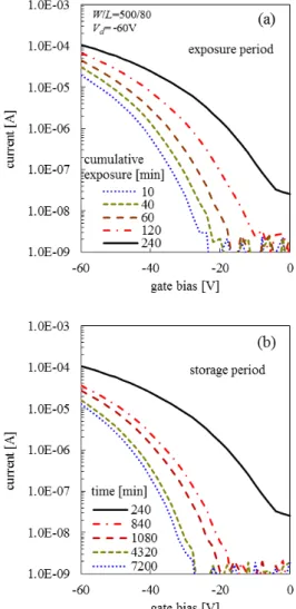
Fig. 1 Transfer characteristics of a C8-BTBT transistor measured under dark during the exposure period (a) and the storage period (b). The legend indicates the cumulative exposure in (a) and the time elapsed under dark in (b). The drain bias was fixed at−60 V. The channel length and width are indicated in the figure.
channel width and length of the transistor used in this exper- iment were 500μm and 80μm, respectively. The thickness of the semiconductor layer was 100 nm.
The transistor was exposed to blue laser light for 5 min in air at room temperature. The wavelength and the irradi- ance were 408 nm and 10 mW/cm2, respectively. No bias was applied to the transistor during the exposure. Transfer and output characteristics were measured under dark. This exposure and characterization cycle was repeated so that the cumulative exposure time reached 240 min. Then the tran- sistor was stored in a nitrogen-filled desiccator under dark and it was taken out for characterization at selected times.
The results are shown in Fig. 1. The noise level is a little lower than 1 nA due to the source meters used in this mea- surement (Keithley, Model 2400).
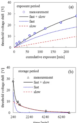
We extracted threshold voltage and mobility by fitting these curves with the standard equation for drain current in saturation regime [22]. The results are shown in Fig. 2. The mobility remains more or less the same. Large positiveVt
Fig. 2 Parameters extracted from the measured transfer curves in Fig. 1.
The abscissa represents the cumulative exposure during the exposure period and the time elapsed under dark during the storage period.
shift is observed during the exposure and the trend is re- versed during the storage period. The threshold voltages extracted from the output curves (not shown) coincide with the data in Fig. 2 [20].
We assume that the blue light generates charged meta- stable states in the channel region. The channel charge in the gradual channel approximation is slightly modified and the density of these states per unit areaNmsis related to the threshold voltage shiftΔVtby,
qNms=CiΔVt, (1)
whereCi is the capacitance of the gate insulator per unit area andqis the elementary charge. To account for its time evolution, we consider the following rate equations with a generation termGand a decay term.
dNms
dt =G−Nms
τ , for 0≤t≤T, (2)
dNms
dt =−Nms
τ , forT <t. (3)
Here, τ is a time constant for the decay andT is the cu- mulative exposure at the end of the exposure period. For simplicity, we ignore the duration required for the electrical characterization. Solutions under the boundary conditions ofNms(0)=0 andNms(T)=N0, are simple expressions con- taining an exponential function, which cannot fit the data in Fig. 2. Stretched exponential function is often used for fit- ting relaxation phenomena. In place of this phenomenolog- ical approach, we consider a model with two types of meta- stable states decaying independently. Now the expressions forNms(t) is given as follows.
Nms(t)=N0
2
i=1
αi
1−exp (−t/τi)
1−exp (−T/τi), for 0≤t≤T, (4) Nms(t)=N0
2
i=1
αiexp [−(t−T)/τi], forT <t, (5)
α1+α2 =1. (6)
Fig. 3 The two-component model reproduces the temporal behavior of the threshold voltage shift. The same fitting parameters are used for fitting the data during the two periods.
We calculated each component and compared with the data in Fig. 2. As shown in Fig. 3, theVt shift is well de- scribed by the sum of these two components. The same set of parameters (τ1 = 200 min, τ2 = 2000 min, α1 = 0.65, T = 240 min,ΔVt(T) = 28.0V) is used for Figs. 3(a) and (b).
2.2 Onset Voltage Shift
Onset voltageVon is defined as the gate bias at which sub- threshold current starts to flows. This definition is somewhat arbitrary. In practice, we extracted the gate voltages corre- sponding to the drain current of 50 nA and 100 nA from each transfer curve in Fig. 1. In Fig. 4, these are indicated by the triangles and the circles, respectively. Because they are sep- arated by a small fixed amount, the shift inVon (ΔVon) is almost the same for these two definitions.
Because the time evolution ofVonin Fig. 4 is so similar to the behavior ofVtin Fig. 2, it is tempting to use the same functional forms with Eqs. (4)–(6) to fitΔVon. In fact, the result of this fitting (not shown) is almost identical to Fig. 3.
Therefore, the two-component model reproduces the behav- ior of the onset voltage in this experiment. This empirical result is somewhat surprising because there is no explicit ex- pression connecting the charged meta-stable states and the onset voltage. We will discuss this issue in Sect. 4.
Fig. 4 Onset voltage extracted from the transfer curves in Fig. 1. The legend indicates the level of the drain current used for defining the onset voltage.
3. PPC in n-Type Transistor
We observed similar photo-induced effects with two types of top-gate n-type transistors. In this paper, these are denoted as pure or blend devices because their semiconductor layers were inkjet printed with inks made from either a pure solu- tion of perylene derivative or a solution mixed with an in- sulating polymer. Blending an insulator polymer suppresses the coffee ring effect during the film-forming process. In addition, vertical phase separation is expected to improve the channel quality. However, we have not yet been able to determine how the semiconductor material is distributed in this film. More detailed information on these transistors is found in Ref. [16]. For both devices, Vtshift was dramati- cally enhanced when the gate was negatively biased during illumination. A higher temperature accelerated the recovery process for both devices [16].
It is interesting to see if the two-component model de- scribed in Sect. 2 can reproduce the behavior ofVtandVon
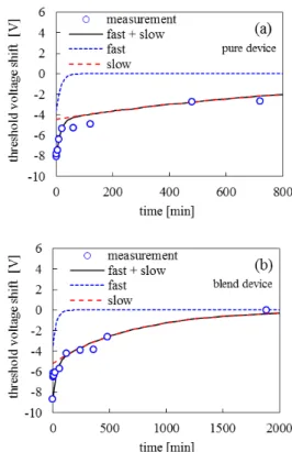
in these transistors. We carried out a similar stress-recovery experiment with two minor changes: (a) a blue LED is used as a light source and (b) the channel region was illumi- nated through their plastic substrates. The irradiance at the channel of a transistor was set to 1 mW/cm2. The transis- tors were exposed to the blue light for 1 min under the gate bias of−20 V. We monitored the recovery process after this single stress event with a source meter and a picoammeter (Keithley, Model 2400 and Model 6487). Transfer curves obtained at selected times are shown in Figs. 5(a) and (b) for a pure and blend device, respectively.
We extract threshold voltage and mobility from the re- gions of the curves in Fig. 5 where the gate bias is clearly beyond the threshold voltage. These transfer curves are slightly curved in linear plot. Therefore, we have adjusted the gate voltage range for each curve so that a similar level of drain current flows. Even with this adjustment, bumpy features appear in the extracted parameters as shown in Fig. 6. Nevertheless, the same trend with the right hand
Fig. 5 Transfer characteristics of the two n-type transistors. The legend indicates the time elapsed after the stress. The drain bias was fixed at 5 V.
The channel length and width are indicated in each figure.
side of Fig. 2 is still observed for these n-type transistors:
the threshold voltage shifts recover with time after the stress while the mobility is not affected.
We start the same analysis by assuming two meta- stable states (fast and slow component). In this case, the recovery process starts att=0. With a slight modification in the boundary condition, the following equation is obtained.
Nms(t)=N0αexp (−t/τ1)+(1−α) exp (−t/τ2) (7) The parameterα(0< α <1) represents the ratio of the two components att=0.
The threshold voltage shift ΔVt is related toNms via Eq. (1). We calculatedΔVtand compared with the measure- ment in Fig. 7. The solid lines represent the sum of the two calculated components and they reproduce the measurement well. Table 1 summarizes fitting parameters used for each n-type transistor and for the C8-BTBT transistor described in Sect. 2.
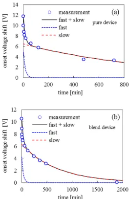
Next, we attempt to fit onset voltages of these n-type transistors. In this case, we define onset voltage as the gate bias at which the drain current exceeds 10 nA. This defini-
Fig. 6 Threshold voltage and mobility extracted from Fig. 5. The thresh- old voltage slowly returns to its initial value for each device. The blend device shows slower recovery.
Fig. 7 The two-component model reproduces the temporal behavior of the threshold voltage shift in the two n-type transistors. The parameter set is different for the two devices.
tion is again somewhat arbitrary but we can still discuss the behavior of the shiftΔVon. The values extracted from Fig. 5 are shown in Fig. 8. The same parameter set is used for fit- tingΔVtandΔVonfor each device as summarized in Table 1.
Fig. 8 Onset voltages extracted from Fig. 5. In both devices, the onset voltage slowly returns to initial values. The recovery is slower for the blend device.
Fig. 9 The temporal behavior of the onset voltage shift is reproduced by the two-component model. For each device, the same parameter set is used for fittingΔVtandΔVon.
4. Discussion
The model assuming charged meta-stable states in the grad- ual channel approximation is for the on current only. It ap- plies for the shift in the threshold voltage but not for the onset voltage. However, a common parameter set repro- duces time evolution of Vt and Von for each of the three types of transistors examined here. This is due to the fact
Fig. 10 Correlation between the photo-induced shifts inVonandVtfor the three transistors in our experiment as well as for the pentacene transistor in Ref. [11]. Correlation coefficient and gradient of the linear fitting are indicated for each data set.
that changes inVtare well correlated to those inVonin these experiments on photo-induced effects. This empirical fact is clearly shown in Fig. 10 where the open circles, triangles and squares represent the data from these transistors. Also plotted is the data set for a pentacene transistor [11]. Corre- lation coefficient and gradient of the linear fitting are indi- cated for each data set.
Sub-threshold current has been analyzed numerically [11] and some analytical expressions have been proposed for circuit simulations [23], [24]. A qualitative understanding of sub-threshold current is as follows. There is no charge ac- cumulation at the interface with the gate insulator when the gate electrode is biased below the threshold voltage. Sub- threshold current flows in the bulk material when a conduct- ing path exists. The current varies as the resistivity of this region is altered by the gate bias. When the amount of fixed space charges increases in this region, the gate voltage re- quired for this partial depletion becomes larger and the sub- threshold current increases.
As shown in Fig. 10, the gradient of the linear fitting for the C8-BTBT transistor is very close to unity. Lateral translation of the initial transfer curve in Fig. 1 reproduces most parts of the other curves. This suggests that the meta- stable space charges exist in a sheet-like form at the interface between the gate insulator and the semiconductor, blocking the effect of the gate bias. In case of the n-type transistors, the gradient is larger than unity and the onset voltage is more sensitive to the illumination than the threshold voltage. It is likely that the meta-stable space charges are distributed in the semiconductor.
One would wonder what the origins for the two com- ponents are. Phonon-assisted relaxation process observed in these n-type transistors [16] suggests that these are traps.
One possible origin might be some irregular molecular ar- rangements at the interface as well as in the bulk. These sites could generate deep and shallow states. Because the electronic structures would be different at the interface from the bulk, two types of trap states might result. In addi-
tion, heavy impurity atoms might precipitate at the inter- face of a bottom-gate transistor during a solution process and form some complexes that become charged upon illu- mination. Further experiment and analysis are needed to test these speculations.
Finally, it is reasonable to expect that these photo- induced effects depend on the quality of the semiconductor film. For the n-type transistors, mixing an insulating poly- mer to the semiconductor solution altered the recovery pro- cess. As for the C8-BTBT transistors, the thermal treatment induced phase change in the spin-coated films. Polarized microscope observation revealed optical anisotropy in these thermally-treated films [25]. The field-effect mobility of our transistors is of the order of 1cm2/Vs. These facts suggest that the C8-BTBT molecules are reasonably well packed and that they are oriented along a certain direction. Temperature gradient can be utilized to control the direction of this phase change [26]. Although we have not yet been able to vary its film quality in a systematic manner, it would be interesting to see how the photo-induced effects manifest themselves in transistors with improved semiconductor crystallinity.
5. Conclusion
In a p-type top-contact C8-BTBT transistor, positive shifts of both threshold voltage and onset voltage are observed.
The shifts in these voltages add up after each illumination step and recover under dark. We have used a model with two charged meta-stable states decaying independently to account for this behavior. The same parameter set repro- duces the time evolution of the threshold voltage during the build-up phase and the recovery phase. The behavior of the onset voltage is also reproduced by the same parameters due to the empirical fact that these two voltage shifts are well correlated. We have also studied photo-induced effects in n-type top-gate transistors based on a perylene derivative.
The threshold voltage and the onset voltage shift in the neg- ative direction upon illumination under a negative gate bias and they recover under dark. The two-component model re- produces the time evolution of these shifts. They are also well correlated in these transistors. The onset voltage shift is more sensitive to the illumination than the threshold volt- age shift. This sensitivity differs among the transistors and it might give some ideas on how these meta-stable sites are distributed.
Acknowledgments
We thank Yuuske Suenaga for synthesizing the C8-BTBT material. Our gratitude is extended to Ryohei Yamanaka, Junpei Nishiyama and Munehisa Matsuda for their assis- tances in the electrical characterization.
References
[1] R.A. Street, “Thin-film transistors,” Adv. Mater., vol.21, pp.1–16, 2009.
[2] Z. Bao and J. Locklin, Organic Field-Effect Transistors, CRC Press, Taylor & Francis Group, 2007.
[3] E. Fortunato, P. Barquinha, and R. Martins, “Oxide semiconduc- tor thin-film transistors: A review of recent advances,” Adv. Mater., vol.24, pp.2945–2986, 2012.
[4] R.L. Hoffman, B.J. Norris, and J.F. Wager, “ZnO-based transparent thin-film transistors,” Appl. Phys. Lett., vol.82, pp.733–735, 2003.
[5] K. Ghaffarzadeh, A. Nathan, J. Robertson, S. Kim, S. Jeon, C. Kim, U-I. Chung, and J.-H. Lee, “Persistent photoconductivity in Hf-In- Zn-O thin film transistors,” Appl. Phys. Lett., vol.97, 143510, 2010.
[6] K. Nomura, T. Kamiya, and H. Hosono, “Interface and bulk ef- fects for bias-light-illumination instability in amorphous-In-Ga-Zn- O thin-film transistors,” J. Soc. Information Display, vol.18, pp.789–
795, 2010.
[7] S.-E. Ahn, I. Song, S. Jeon, Y.W. Jeon, Y. Kim, C. Kim, B. Ryu, J.- H. Lee, A. Nathan, S. Lee, G.T. Kim, and U-I. Chung, “Metal oxide thin film phototransistor for remote touch interactive displays,” Adv.
Mater., vol.24, pp.2631–2636, 2012.
[8] K.S. Narayan and N. Kumar, “Light responsive polymer field-effect transistor,” Appl. Phys. Lett., 79, vol.1891, 2001.
[9] A. Salleo and R.A. Street, “Light-induced bias stress reversal in polyfluorene thin-film transistors,” J. Appl. Phys., vol.94, pp.471–
479, 2003.
[10] S. Ogawa, T. Naijo, Y. Kimura, H. Ishii, and M. Niwano, “Pho- toinduced doping of organic field effect transistors studied by displacement current measurement and infrared absorption spec- troscopy in multiple internal reflection geometry,” Jpn. J. Appl.
Phys., vol.45(1B), pp.530–533, 2006.
[11] A.R. V¨olkel, R.A. Street, and D. Knipp, “Carrier transport and den- sity of state distributions in pentacene transistors,” Phys. Rev. B, vol.66, 195336, 2002.
[12] C. Feng, T. Mei, and X. Hu, “Influence of trapping states at the dielectric-dielectric interface on the stability of organic field- effect transistors with bilayer gate dielectric,” Org. Electron. vol.12, pp.1304–1313, 2011.
[13] V. Podzorov, V.M. Pudalov, and M.E. Gershenson, “Light-induced switching in back-gated organic transistors with built-in conduction channel,” Appl. Phys. Lett., vol.85, pp.6039–6041, 2004.
[14] N. Mathews, D. Fichou, E. Menard, V. Podzorov, and S.G.
Mhaisalkar, “Steady-state and transient photocurrents in rubrene single crystal free-space dielectric transistors,” Appl. Phys. Lett., vol.91, 212108, 2007.
[15] M. Barra, F. Bloisi, A. Cassinese, F.V. Di Girolamo, and L. Vicari,
“Photoinduced long-term memory effects in n-type organic perylene transistors,” J. Appl. Phys., vol.106, 126105, 2009.
[16] T.N. Ng, I. Fujieda, R.A. Street, and J. Veres, “Persistent photocon- ductivity effects in printed n-channel organic transistors,” J. Appl.
Phys., vol.113, 094506, 2013.
[17] H. Ebata, T. Izawa, E. Miyazaki, K. Takimiya, M. Ikeda, H. Kuwabara, and T. Yui, “Highly soluble [1]benzothieno[3,2- b]benzothiophene (BTBT) derivatives for high-performance, sol- ution-Processed organic field-effect transistors,” J. Am. Chem. Soc., vol.129, 15732, 2007.
[18] H. Minemawari, T. Yamada, H. Matsui, J. Tsutsumi, S. Haas, R.
Chiba, R. Kumai, and T. Hasegawa, “Inkjet printing of single-crystal films,” Nature, vol.475, pp.364–367, 2011.
[19] J.E. Northrup, “Two-dimensional deformation potential model of mobility in small molecule organic semiconductors,” Appl. Phys.
Lett., vol.99, 062111, 2011.
[20] T. Hoshino, S. Kitahama, T. Hiraki, I. Fujieda, Y. Suenaga, and T. Hanasaki, “Light-induced effect on electrical charac- teristics of a transistor based on 2,7-dioctyl[1]benzothieno[3,2- b][1]benzothiophene,” presented at the International Conference on Flexible and Printed Electronics, Tokyo, Sept. 2012.
[21] I. Fujieda, T. Hohsino, and T. Hanasaki, “A model for photo-induced threshold voltage shift in a transistor based on a BTBT derivative,”
Proc. IDW/AD’12, pp.959–960, Dec. 2012.
gawa, paper number 28p-PA8-11 (in Japanese), March 2013.
Ichiro Fujieda received his B.S. in physics from Waseda University in 1981 and Ph.D. in nuclear engineering from the University of Cal- ifornia, Berkeley in 1990. From 1990 to 1992 he was a research associate at Xerox Palo Alto Research Center. For the next 11 years, he was with NEC. He has been a professor at Rit- sumeikan University since 2003.
Tse Nga Ng received her B.A. in chem- istry from Knox College in 2000 and Ph.D. in physical chemistry from Cornell University in 2006. She has been working at Palo Alto Re- search Center since 2006, and she is currently Senior Member of Research Staff.
Tomoya Hoshino received his B.S. de- gree from the department of photonics at Ritsumeikan University in March 2012. He is currently a graduate student and is engaged in research related to organic electronics.