Yasuo KOIDE
††, Nonmembers, Yoshinori WATANABE
††, Member, Nobuhiko OZAKI
†††, Shunsuke OHKOUCHI
††††, Tsuyoshi NOMURA
†††††, Daisuke INOUE
†††††, Nonmembers, Takayuki MATSUI
†††††, Member, Atsushi MIURA
†††††, Hisayoshi FUJIKAWA
†††††, Nonmembers, and Kazuo SATO
†††††, Member
SUMMARY This paper reviews our recent activities on nanophotonics based on a photonic crystal (PC)/quantum dot (QD)-combined structure for an all-optical device and a metal/semiconductor composite structure using surface plasmon (SP) and negative refractive index material (NIM). The former structure contributes to an ultrafast signal processing component by virtue of new PC design and QD selective-area-growth technologies, while the latter provides a new RGB color filter with a high precision and optical beam-steering device with a wide steering angle.
key words:photonic crystal, quantum dot, surface plasmon, negative index material, all-optical switch
1. Introduction
An integrated optoelectronic device/circuit, developed widely in 1990’s as a planar light wave circuit (PLC), has far advanced in 2000’s along with a proposal of photonic crystals (PCs) and an advanced growth technology of quan- tum dots (QDs) [1], [2]. In addition, appearance of sur- face plasmon (SP) [3] and negative refractive index ma- terial (NIM) [4] have stimulated such trend towards new nano-photonics-based integrated circuits. Figure 1 shows our nano-photonics roadmap predicting potential PC, QD, SP and NIM abilities towards new application fields such as silicon photonics and novel imaging/sensing as well as next generation photonic network system. Based on this map, we have recently verified that an optical nonlinearity (ONL) in the QD significantly contributes to a key role for a PC- based all-optical switch, while SP and NIM are promising for unique applications such as optical nano-antenna, novel RGB color filter and optical beam-steering device. This pa- per reviews such nano-photonic technologies and applica- tions.
Manuscript received June 30, 2011.
Manuscript revised October 18, 2011.
†
The author is with University of Tsukuba, Tsukuba-shi, 305- 8571 Japan.
††
The authors are with National Institute for Materials Science (NIMS), Tsukuba-shi, 305-0047 Japan.
†††
The author is with Wakayama University, Wakayama-shi, 640-8510 Japan.
††††
The author is with NEC Corporation, Tsukuba-shi, 305-8501 Japan.
†††††
The authors are with Toyota Central R&D Labs., Inc., Aichi- ken, 480-1192 Japan.
a) E-mail: [email protected] DOI: 10.1587/transele.E95.C.178
Fig. 1 Key roles, their relevance and road map in our nano-photonics research.
2. Photonic Crystal Nanotechnology
2.1 Photonic Crystal-Based All Optical Switch
The PC, having a wide band gap and strong dispersion [1], exhibits strong optical confinement and light/matter inter- action in the defect waveguide. The QD, having a high density-of-state [2], exhibits large ONL such as absorption saturation under low pumping energy. We have proposed all-optical switches with a PC and QD combined symmet- rical Mach-Zehnder (SMZ) configuration [5], named PC- SMZ (analogue switch) and PC-FF (digital flip flop switch) [6]. An ultrafast operation principle and schematic diagram of the PC-SMZ are shown in Figs. 2(a) [5] and (b) [6]. A
“switch-on” control pulse (CP) incident in the upper ONL
arm causes nonlinear (absorption saturation in the QD in
this case) optical refractive index change, δn, leading to a
phase shift φ
1= 2π(δn/λ)l
ONLfor a series of signal pulses,
where λ is a wavelength of the signal pulse and l
ONLis an
ONL arm length. The phase shift φ
2is generated similarly
in the lower ONL arm by the “switch-off” control pulse. As
a result, a phase-shift di ff erence Δ φ = | φ
1− φ
2| is generated at
the combined Y-junction. Only when Δ φ = π /2 or π, the sig-
nal pulses are switched spatially. Time response of the δn is
rapid (sub-ps) in rise but slow (sub-ns) in fall in the semicon-
ductor. However, since the δn is excited time-differentially,
Copyright c 2012 The Institute of Electronics, Information and Communication Engineers
Fig. 2 (a) All-optical switching principle. (b) Schematic diagram. (c) Time-differential phase shift responses pumped by the on-CP and off-CP.
(d) Phase shift difference between two identical arms in the PC-SMZ.
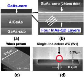
Fig. 3 Cross sectional SEM images of the PC-SMZ. (a) GaAs/AlGaAs layers. (b) Magnified GaAs core layer including InAs QD layers. (c) The whole chip pattern. (d) Magnified cleaved PC waveguide.
the δn in the tailing slow component are cancelled, so that the PC-SMZ is operated as a time-di ff erential phase modu- lator [5], [6]. Figures 2(c) and (d) show time differences of the δn’s in the upper / lower ONL arms and the resultant dif- ference of the phase shift Δ
φ= Δ φ
on− Δ φ
off, respectively.
In this sense, the SMZ device has a rectangular-like time re- sponse with sharp abruptness. We have so far demonstrated single switching by single on- and o ff -CPs at 2-ps-rise / fall times in as low as 10–100 fJ switching energy [7].
2.2 Photonic Crystal Waveguide Structure
Our PC waveguide is composed of an air-bridge type slab waveguide with single line defect, as shown in Fig. 3. Figure 3(a) shows a cross section of MBE-grown GaAs/AlGaAs epitaxial layers on the GaAs substrate, while Fig. 3(b) shows a magnified GaAs-core (PC waveguide) layer with four InAs-QD layers embedded in it. The air-
Fig. 4 Computational model of the TO design including the design domain.
bridge type PC waveguide is fabricated by eliminating a sac- rificial AlGaAs layer. Figures 3(c) and (d) show a cross sec- tional PC-SMZ chip and magnified cross section of the PC waveguide area, respectively. A solid line circle in Fig. 3(d) shows a cross section of about 0.7-μm-wide and 0.25-μm- thick single-line defect PC waveguide [8].
2.3 Advanced Photonic Crystal Waveguide Design For implementation of the PC-SMZ and PC-FF, a new de- sign method called topology optimization (TO) has been de- veloped for improving band-narrowed non-straight waveg- uides into wide / flat-band waveguides in the PC-SMZ. It requires intersection, bend, λ-selective Y-junction and di- rectional coupler (DC) waveguides as non-straight waveg- uides. The TO technology and experimental results are shown later.
As shown in Fig. 4, the TO procedure is performed to
maximize transmittance in a straightforward line (indicated
in arrows) by modifying refractive index distributions in the
design domain indicated by solid circles. For more details,
see other descriptions [9], [10]. The TO design has so far
been applied to intersection [11], bend [12], wavelength-
selective Y-junction [13], DC [14] waveguides and the dra-
matic improvement of this method has been experimentally
verified. Here, application of the TO method for designing
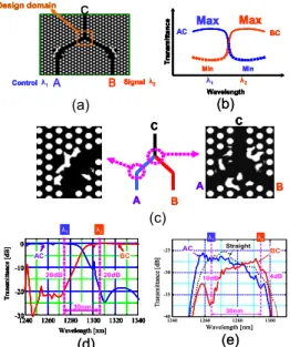
the wavelength-sensitive Y-junction is shown. In Figs. 5(a)
and (b), the TO method was adopted to (1) maximize the
transmittances along AC and BC channels, (2) minimize the
transmittance along unwanted AB and BA channels, and (3)
optimize them at two separate (by 30 nm in this case) wave-
lengths. TO designed unique air-hole patterns are shown in
Fig. 5(c). Comparison of calculated transmission spectra be-
tween AC and BC channels at 30-nm-apart wavelengths re-
sult in 20 dB isolation, as shown in Fig. 5(d), while Fig. 5(e)
shows corresponding measured transmission spectra along
the channels AC and BC. The results are well reproducing
the calculation mentioned above, although the isolation is
not enough. The result is realized for the first time by the
TO method and almost impossible by the conventional de-
sign method. The result is also essential for designing the
wavelength-selective Y-junction used in the PC-FF.
Fig. 5 (a) Computational model of the TO-designed Y-junction. (b) Schematic picture of the required asymmetric transmission spectra. (c) SEM images of the bend (left) and Y-junction (right) parts in the fabricated TO-designed waveguides. (d) and (e) Respective calculated and measured transmission spectra of the channels AC and BC in the TO-designed Y- junction.
Fig. 6 (a) Pseudo-flip-flop operation of the PC-SMZ. (b) Remarkable on- state decaying for a large set-reset pulse distance in (a). (c) Clock pulse refreshment-induced optical bi-stability in the PC-SMZ. (d) Resultant flip- flop pulse operation in (c).
2.4 Photonic Crystal Waveguide Based All-Optical Flip- Flop
Taking into account the principle of the time-differential phase-modulator of the PC-SMZ, it reminds us of the sim- ilarity to the flip-flop (FF) operation, as shown in Fig. 6(a), because “switch-on” and “switch-off” control pulses serve as “set” and “reset” pulses. However, when the “reset”
pulse is far delayed from the “set” pulse, the decay of the
“on” state is remarkable due to the carrier relaxation in the QD, so that a complete bi-stable state is difficult to main- tain, as shown in Fig. 6(b). For improving this problem, we introduce a series of clock pulse for refreshment of the decaying “on” state between control pulses, as shown in
Fig. 7 Configuration of the PC waveguide and areas of QDs with different absorption wavelengths in the PC-FF.
Fig. 6(c), which shows an operational principle of an opti- cal bi-stability in the PC-FF evolved from the PC-SMZ, as indicated by a resultant flip-flop pulse shape in Fig. 6(d) [6].
The proposed optical flip-flop is available by the wave- guide configuration in Fig. 7. Two identical PC-SMZs (SW- 1 and SW-2) [6] are coupled by a feedback loop supporting the bi-stability. This device is hereinafter referred to simply as PC-FF. In this scheme, the delay time on the feed-back loop should be reduced to as short as ps if the period of the “on” state is less that 10 ps corresponding to more than 40 Gb/s switching speed.
Since the total length of the PC waveguides in the PC- FF is as short as several 100 μm (corresponding to several ps delay time), the PC-FF is capable of operation at more than 40 Gb/s switching speed.
The principle of the PC-FF has been verified so far by computer simulation [6]. For the calculation, a period and width of set-reset pulses were 100–25 ps and 32–8 ps, re- spectively, while the repetition rate of the clock pulse, delay time for the feed-back loop and carrier relaxation time were 100–25 ps, 10 ps and 100–25 ps, respectively. For these pa- rameters, the PC-FF was operated successfully at the speed of 10–40 Gb / s and eye patterns were clearly opened [15].
3. Quantum Dot Nanotechnology for All-Optical Switch
3.1 Selective-Area-Growth of Quantum Dot
Recent development of self-assembled InAs QDs has at-
tracted a great deal of attention because of its potential for
use in telecommunication systems. As indicated in Fig. 2,
the PC-SMZ requires InAs QDs partially embedded in the
GaAs PC waveguide as ONL materials. Specifically, the
PC-FF requires two separate QD sites, as shown in Fig. 7,
where a QD ensemble with the wavelength λ
1= 1.29 μm in
SW-1 and QD ensemble with the wavelength λ
2= 1.31 μm
in SW-2 are grown several tens-hundreds apart on a chip
for example [6]. For this purpose, selective-area-growth
(SAG) of QDs has been developed by using a metal-mask
(MM) method [16], [17]. Wavelength of the SAG-QD can
be controlled by the thickness of an inserted InGaAs layer
as a stress reducing layer (SRL) between the InAs-QD and
GaAs-spacer layer [18].
Fig. 8 (a) MM configuration in the MBE growth chamber. (b) Atomic force micrograph (AFM) image of the QD ensemble on the unmasked re- gion. (c) PL peak showing high uniformity of the QD ensemble.
Fig. 9 (a) Optical microscope photograph of the rotatable MM mounted in the substrate holder. (b) Two different positions of the MM before and after 180◦rotation of the MM for SAG of QD1 and QD2.
Fig. 10 (a) Optical microscope photograph of PC-SMZ waveguide. (b) PL intensity mapping at separate colour zones in QD-1 and QD-2 areas.
(c) PL spectra at QD-1 and QD-2 areas, showing different wavelengths for QD-1 and QD-2.
Figure 8(a) shows an MM configuration in the MBE growth chamber, while Fig. 8(b) shows a typical atomic force micrograph (AFM) image of the QD ensemble on the unmasked region grown by the MM method. The QD den- sity is as high as 4×10
10/cm
2. QD uniformity is estimated to be 28 meV in term of FWHM (full width at half maximum) in the PL peak, as shown n Fig. 8(c).
SAG for the separate QD ensemble is carried out as fol- lows: The MM is designed to be 180
◦rotational on the MBE wafer holder, as shown in Fig. 9(a) [19]. After the QD1 en- semble is grown, as illustrated in Fig. 9(b), an In
0.2Ga
0.8As layer is deposited on the QD and capped with a GaAs layer.
Then, the MM is rotated by 180
◦and the QD2 is grown in the same manner except for the thickness of SRL. The SRL thickness is set to 2.7 nm for the QD1 and 4.5 nm for the QD2, respectively.
Figure 10(a) shows an optical microscope photograph of fabricated two sets of PC-SMZ waveguides designed in
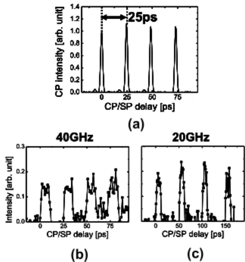
Fig. 11 (a) Input four-pulse train with a period of 25 ps used for se- quential operation for the PC-SMZ. (b) and (c) Output pulses in sequential switching with repetition frequencies at 40 and 20 GHz, respectively.
the 300 μm × 500 μm chip. Two shadowed areas indicate positions of the buried QD-1 with 1.29-μm wavelength and QD-2 with 1.31-μm wavelength. Areas of the QD-1 and QD-2 were identified by the PL intensity mapping, as shown by the two separate zones in Fig. 10(b) [19]. Both QD-1 and QD-2 are located as designed on the PC waveguides. In ad- dition, control of different wavelengths for QD-1 and QD-2 were confirmed to be designed as 1,290 and 1,310 nm, re- spectively, as shown by the PL spectra in Fig. 10(c). Exper- imental demonstration of the ultra-fast all-optical switching by the PC-SMZ and current problems for succeeding optical FF operation by using the PC-FF are discussed in the next section.
3.2 Ultra-Fast Operation and Future Challenge of PC/QD All-Optical Switch
An optical switching response of the PC-SMZ is shown here. In 2004, a successful switching operation pumped by a set of on-pulse and o ff -pulse was reported [7], [20], [21].
Resultant rise and fall times were as fast as ∼2 ps and input pulse energy was as low as 100 fJ. Modulation (switching ratio) was 50%, half the desired value (100%) due to the deficient phase shift Δ φ of π /2 and not π. Recently, high repetition-rate operation of the PC-SMZ has been demon- strated by using an input four-pulse train with a period of 25 ps. The results are shown in Fig. 11(a). Two cases of rep- etition frequencies at 40 and 20 GHz were demonstrated, as shown in Figs. 11(b) and (c), respectively [22]. A switch- ing ratio in this experiment was as low as 16%. A possible improvement of the switching ratio is discussed later.
For sequential operation with repetitive sets of on-/off-
CPs, we have to investigate detailed relationship between
the sequential CP rate and temporal change of the Δ
φheight,
as shown in Fig. 2(d). Otherwise, the Δ
φcould be gradually
decreased below 180˚ due to the decreasing Δ
φ, that is, due
to the carrier accumulation effect caused by the following
density) QD populations in the QD/PC waveguides, respec- tively. (c) and (d) show accumulations of the phase shifts for cases in (a) and (b), respectively. See Ref. [22] for detailed discussions. The resultant Δ
φιdefined by Δ φ
i−on− Δ φ
i−offremains constant or decays gradually depending on the re- lationship between a repetitive-rate of the pumping and the available number of the QDs, as shown in (e) and (f). The switching can be operated completely or incompletely ac- cording to these situations. So far, the waveguide was de- signed as to achieve the low group velocity for enhancing light / matter interaction, thus increasing the ONL at the QD arms [23].
For detailed mechanisms and characterized results of the ONL for the current QD sample in detail, see Ref. [22].
In the current experiment, however, switching modulation was as low as 16% due to un-optimized waveguide parame- ters including low group velocity. In the new design, 100%
modulation is to be achieved at 40 GHz by increasing the QD layer, n
g(reciprocal of group velocity) and QD arm.
Regarding the PC-FF, it is noted that, in spite of suc- cessful ultrafast all-optical switching of the PC-SMZ, op- eration of the PC-FF was not confirmed experimentally by the current sample. Main reason is that the value of the
Fig. 12 Schematic pictures showing the condition for the constant phase shift difference independent of carrier accumulation in QDs. (a) and (b) Relationship between the originally grown QD state and QDs pumped by the CP. (c) and (d) Accumulated phase shift induced by the sequential CPs.
(e) and (f) Sequential phase-shift difference between the two arms in the PC-SMZ.
vice from the practical application view point.
4. Surface-Plasmonic Nanotechnologies
Surface plasmon (SP) is a light wave propagating at the metal/dielectric boundary as a result of coupling to the elec- tron motion in the metal. Since energy of the SP is con- fined in the interface, enhanced ONL in nano-scale and other interesting phenomena and applications have been reported recently. One of the unique features of the SP is an extra- ordinary transmission of light incident on a nano-scale via- hole on a metal/dielectric material [3], [24], [25]. It can be applied to an RGB color filter with high precision. Recent experimental results of such a device in an aluminum-film hole-array is shown here [26]–[28]. Figure 13 is a target- ing picture. Usage of the aluminum enables RGB color filters covering a shorter wavelength as a result of a high plasma frequency than in use of silver and gold. In addition, nanofabrication of aluminum materials has been matured by the conventional semiconductor technologies.
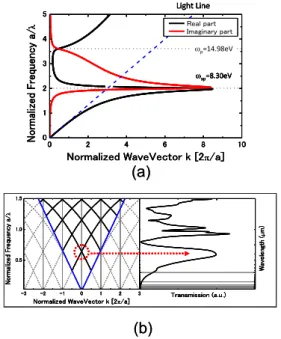
Figure 14(a) shows a dispersion relation of the SP in an aluminum / SiO
2system calculated by the Lorentz-Drude model. The SP generates in the frequency range below ω
sp(8.30 eV), while ω
sp< ω < ω
p(14.98 eV) and ω
p< ω cor- respond to absorptive and transparent regions for the light, respectively. In the periodic structure, on the other hand, the SP is subject to a band diagram as a result of Bloch func- tion, as shown at the left hand side in Fig. 14(b). In the fig- ure, the transmission spectrum at the Γ point is shown also.
The large peak indicated by the dotted arrow corresponds to the energy of the SP used in the experiment. Samples were triangle-lattice air-hole arrays with a unit circle hole pattern, where lattice constant a = 240–420 nm (a / λ = 0.6, λ
= 400–700 nm). Final aluminum hole-array patterns on the glass were covered with SiO
2layer. Figure 15 shows mea- sured optical transmission spectra for samples with different lattice constants in an air-hole array. The light source was
Fig. 13 Schematic picture of an RGB color filter comprising an aluminum-film hole-array.
Fig. 14 (a) Dispersion relation of the SP in an aluminum/SiO2system.
(b) Dispersion relation of the SP in a periodic structure (left) and transmis- sion spectrum at theΓpoint (right).
Fig. 15 Measured optical transmission spectra for samples with different lattice constants in an air-hole array.
a halogen lamp (white light), while a detector was a CCD camera. A transmitted color (wavelength) has been found to agree with a calculated result in the band diagram. In this way, an SP induced RGB color filter with high color (wave- length) selectivity has been demonstrated for the first time.
5. Negative Refractive Index Material with Metal/
Dielectric Composites
A negative refractive index material (NIM) is one of the re- cent topics in the nano-photonic field as indicated in Fig. 1 [4], [29]–[35]. Recently we proposed a planar-prism type beam steering device using NIM which is available in an infrared wavelength region (1.55 μm) [36]. The negative re- fractive index effect generates at a composite structure of multi-stacked aluminum (Al) metal layers embedded in the host SiO
2medium. An air-hole array with sub-wavelength
Fig. 16 Schematic diagram of the planar prism with graded NIM for near infrared beam steering.
Fig. 17 Calculated band diagrams of the planar prism with varied curvatures of corners at the square holes.
shapes in size is formed in the plane. The beam steering is caused by the air-hole shape changing side by side from circle to square in the steering direction. Figure 16 shows a schematic diagram of the device. The detailed structure is as follows: In the thickness direction, the structure has five stacked aluminum/SiO
2composite layers. Each unit layer has 20-nm-thick Al film and 80-nm-thick SiO
2, thus form- ing alternative Al / SiO
2layers with a period (d) of 100 nm.
Dispersion effect of this structure exhibits the negative re- fractive index behaviour because the product of the phase velocity and group velocity on the dispersion curve is neg- ative, as shown later. The secret of this device is that the dispersion is gradually controlled side by side due to the spatially changing air-hole shape.
Figure 17 shows dispersion curves for a stacked com-
posite with 1 μm × 1 μm square and single air-hole in it. In
order to form a graded index distribution, a curvature, R, of
the square corner in the air-hole is gradually changed from
0 to 250 nm, as shown by the different dispersion curves in
Fig. 17. In the lateral direction on the device plane, such
elements with di ff erent hole shapes are gradually arranged,
e.g., 10 by 10 with a 1-μm-pitch over the entire plane. For
this structure, simulated results of the electromagnetic wave
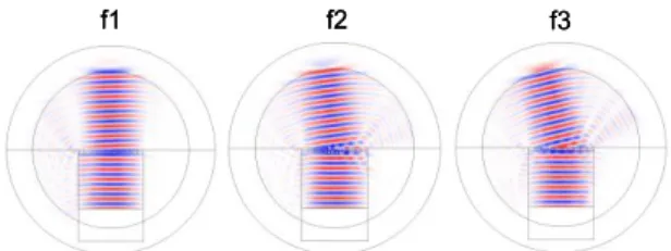
propagation at the three different normalized frequencies, f1
(0.990), f2 (0.965) and f3 (0.940), are shown in Fig. 18. In
the figure, when the frequency is changed from f1 to f3, a ra-
diated angle of the output beam is changed from 0
◦to 12.5
◦Fig. 18 Simulated electromagnetic wave propagations at the correspond- ing frequencies, f1, f2 and f3 in Fig. 16 (in unitω).
due to the graded index distribution e ff ect, although the de- tailed procedure for derivation from the dispersion curve to the radiated angle is omitted here. Thus, beam steering behaviour in this structure is clearly shown. Alternatively, for practical application, output beam angle is changed by changing the refractive index of the liquid crystal infiltrated in the air-hole by applying the external electric or magnetic field. The planar prism is achieved in this way.
6. Conclusion
Our resent research on nano-photonics involving the PC, QD, SP and NIM has been reviewed. For PC/QD-combined devices, new topology optimization method for design of high performance PC waveguides and novel selective-area- growth method for QD-containing advanced photonic inter- graded circuits have been developed and applied to ultrafast and low-energy all-optical switches using ONL in the QD- embedded waveguide. On the other hand, SP has been in- vestigated for a novel plasmonic RGB color filter. Finally, negative refractive index in the stacked metal / dielectric composite with an air-hole array has been applied to an op- tical beam-steering device with a wide range of steering an- gle. These nano-photonics will pave the road to novel sens- ing / imaging components as well as new integrated signal processing components/circuits in a next generation pho- tonic network system.
Acknowledgement
Authors would like to acknowledge kind contributions of A. Watanabe, S. Nakamura, Y. Nakamura, H. Nakamura, K. Kanamoto, Y. Tanaka, Y. Takata and Y. Kitagawa. Re- search works reviewed here were partly supported by the New Energy and Industrial Technology Development Orga- nization (NEDO), a Grant-in-Aid from the Ministry of Ed- ucation, Culture, Sports, Science and Technology (MEXT), and Nanotechnology Network Program of MEXT, Japan.
References
[1] E. Yablonovitch, “Inhibited spontaneous emission in Solid-state physics and electronics,” Phys. Rev. Lett., vol.58, no.20, pp.2059–
2062, May 1987.
[2] Y. Arakawa and H. Sakaki, “Multidimensional quantum well laser and temperature dependence of its threshold current,” Appl. Phys.
Lett., vol.40, no.11, pp.939–941, June 1982.
[3] T.W. Ebbesen, H.J. Lezec, H.F. Ghaemi, T. Thio, and P.A. Wolff,
[5] K. Tajima, “All-Optical Switch with Switch-OffTime Unrestricted by Carrier Lifetime,” Jpn. J. Appl. Phys., vol.32, no.12A, pp.L1746–
L1749, Dec. 1993.
[6] K. Asakawa, Y. Sugimoto, Y. Watanabe, N. Ozaki, A. Mizutani, Y.
Takata, Y. Kitagawa, H. Ishikawa, N. Ikeda, K. Awazu, X. Wang, A.
Watanabe, S. Nakamura, S. Ohkouchi, K. Inoue, M. Kristensen, O.
Sigmund, P.I. Borel, and R. Baets, “Photonic crystal and quantum dot technologies for all-optical switch and logic devices,” New J.
Phys., vol.8, 208, 2006.
[7] H. Nakamura, Y. Sugimoto, K. Kanamoto, N. Ikeda, Y. Tanaka, Y.
Nakamura, S. Ohkouchi, Y. Watanabe, K. Inoue, H. Ishikawa, and K. Asakawa, “Ultra-fast photonic crystal/quantum dot all-optical switch for future photonic networks,” Opt. Express, vol.12, no.26, pp.6606–6614, Dec. 2004.
[8] N. Ikeda, Y. Sugimoto, Y. Tanaka, K. Inoue, Y. Watanabe, and K. Asakawa, Semiconductor Science and Technology, vol.22, no.2, pp.149–157, Jan. 2007.
[9] P.I. Borel, L.H. Frandsen, A. Harpøth, J.B. Leon, H. Liu, M.
Kristensen, W. Bogaerts, P. Dumon, R. Baets, V. Wiaux, J. Wouters, and S. Beckx, “Topology optimised broadband photonic crystal Y- Splitter,” Electron. Lett., vol.41, pp.69–71, 2005.
[10] J.S. Jensen, O. Sigmund, L.H. Frandsen, P.I. Borel, A. Harpøth, and M. Kristensen, “Topology design and fabrication of an efficient dou- ble 90-degree photonic crystal waveguide bend,” IEEE Photonics Technol. Lett., vol.17, pp.1202–1204, 2005.
[11] Y. Watanabe, Y. Sugimoto, N. Ikeda, N. Ozaki, A. Mizutani, Y.
Takata, Y. Kitagawa, and K. Asakawa, “Broadband waveguide inter- section with low-crosstalk in two-dimensional photonic crystal cir- cuits by using topology optimization,” Opt. Express, vol.14, no.20, pp.9502–9507, Oct. 2006.
[12] Y. Watanabe, N. Ikeda, Y. Sugimoto, Y. Takata, Y. Kitagawa, A.
Mizutani, N. Ozaki, and K. Asakawa, “Topology optimization of waveguide bends with wide, flat bandwidth in air-bridge-type pho- tonic crystal slabs,” J. Appl. Phys., vol.101, no.11, 113108, June 2007.
[13] Y. Watanabe, N. Ikeda, Y. Takata, Y. Kitagawa, N. Ozaki, Y.
Sugimoto, and K. Asakawa, “Topology optimization of wavelength selective Y-junction for 2D photonic crystal waveguides,” J. Phys.
D, vol.41, no.17, 175109, Aug. 2008.
[14] Y. Watanabe, N. Ikeda, Y. Takata, Y. Kitagawa, N. Ozaki, Y.
Sugimoto, and K. Asakawa, “Wideband operation of 2D pho- tonic crystal directional coupler with topology optimized waveguide bends,” J. Nonlinear Optical Physics & Materials, vol.19, no.4, pp.543–550, Dec. 2010.
[15] S. Nakamura, A. Watanabe, X. Wang, N. Ikeda, Y. Sugimoto, N. Ozaki, Y. Watanabe, and K. Asakawa, “Optical flip-flop based on coupled ultra-small Mach-Zehnder all-optical switches,”
OFC/NFOEC 2008, pp.045–10, San Diego, USA, Feb. 2008.
[16] S. Ohkouchi, Y. Nakamura, H. Nakamura, N. Ikeda, Y. Sugimoto, and K. Asakawa, “Selective growth of high quality InAs quan- tum dots in narrow regions using in situ mask,” J. Cryst. Growth., vol.293, no.1, pp.57–61, July 2003.
[17] N. Ozaki, Y. Takata, S. Ohkouchi, Y. Sugimoto, Y. Nakamura, N.
Ikeda, and K. Asakawa, “Selective area growth of InAs quantum dots with a metal mask towards optical integrated circuit devices,” J.
Cryst. Growth., vol.301-302, pp.771–775, April 2007.
[18] S. Ohkouchi, Y. Nakamura, H. Nakamura, and K. Asakawa, “Con- trol of InAs quantum dot emission wavelengths in narrow regions by selective formation of GaInAs covered layers grown with in situ
mask,” Jpn. J. of Appl. Phys., vol.44, no.7B, pp.5677–5679, July 2005.
[19] N. Ozaki, Y. Takata, S. Ohkouchi, Y. Sugimoto, N. Ikeda, and K.
Asakawa, “Selective-area-growth of InAs-QDs with different ab- sorption wavelengths via developed metal mask/MBE method for integrated optical devices,” Appl. Surf. Sci., vol.254, pp.7968–7971, May 2008.
[20] H. Nakamura, S. Nishikawa, S. Kohmoto, K. Kanamoto, and K.
Asakawa, “Optical nonlinear properties of InAs quantum dots by means of transit absorption measurements,” J. Appl. Phys., vol.94, no.2, pp.1184–1189, July 2003.
[21] H. Nakamura, K. Kanamoto, Y. Nakamura, S. Ohkouchi, H.
Ishikawa, and K. Asakawa, “Nonlinear optical phase shift in InAs quantum dots measured by a unique two-color pump/probe ellipso- metric polarization analysis,” J. Appl. Phys., vol.96, no.3, pp.1425–
1434, Aug. 2004.
[22] Y. Kitagawa, N. Ozaki, Y. Takata, N. Ikeda, Y. Watanabe, Y.
Sugimoto, and K. Asakawa, “Sequential operations of quantum Dot/Photonic crystal All-optical switch with high repetitive fre- quency pumping,” J. Lightwave Technol., vol.27, no.10, pp.1241–
1247, May 2009.
[23] K. Inoue, N. Kawai, Y. Sugimoto, N. Carlsson, N. Ikeda, and K.
Asakawa, “Observation of small group velocity in two-dimensional AlGaAs-based photonic crystal slabs,” Phys. Rev. B, vol.65, 121308, March 2002.
[24] T. Ishi, J. Fujikata, K. Makita, T. Baba, and K. Ohashi, “Si Nano- Photodiode with a surface plasmon antenna,” Jpn. J. Appl. Phys., vol.44, no.12, pp.L364–L366, March 2005.
[25] C. Genet1 and T.W. Ebbesen, “Light in tiny holes,” Nature, vol.445, pp.39–46, Jan. 2007.
[26] N. Ikeda, D. Tsuya, Y. Sugimoto, Y. Koide, K. Asakawa, A. Miura, D. Inoue, T. Nomura, H. Fujikawa, and K. Sato, “Systematic study on surface plasmon-enhanced extra-ordinary optical transmission in an aluminium-film hole-array,” PECS-VIII, International Sympo- sium on Photonic and Electromagnetic Crystal Structures, Sydney, Australia, #51, April 2009.
[27] D. Inoue, T. Nomura, A. Miura, H. Fujikawa, K. Sato, N. Ikeda, D. Tsuya, Y. Sugimoto, Y. Koide, and K. Asakawa, “RGB color fil- ter comprising aluminum film with surface plasmon enhanced trans- mission through sub-wavelength hole-arrays,” Optical MEMS and Nanophotonics 2009, Clearwater Beach, Florida, ThA5, Aug. 2009.
[28] D. Inoue, A. Miura, T. Nomura, H. Fujikawa, K. Sato, N. Ikeda, D.
Tsuya, Y. Sugimoto, and Y. Koide, “Polarization independent visi- ble color filter comprising aluminum film with surface-plasmon en- hanced transmission through a subwavelength array of holes,” Appl.
Phys. Lett., vol.98, 093113, March 2011.
[29] J. Pendry, “Negative refraction makes a perfect lens,” Phys. Rev.
Lett., vol.85, pp.3966–3969, Oct. 2000.
[30] D.R. Smith, J.B. Pendry, and M.C.K. Wiltshire, “Metamaterials and negative refractive Index,” Science, vol.305, no.5685, pp.788–792, Aug. 2004.
[31] A. Sanada, C. Caloz, and T. Itoh, “Planar distributed structures with negative refractive index,” IEEE Trans. Microw. Theory Tech., vol.52, no.4, pp.1252–1263, 2004.
[32] V.M. Shalaev, W. Cai, U.K. Chettiar, H.-K. Yuan, A.K. Sarychev, V.P. Drachev, and A.V. Kildishev, “Negative index of refraction in optical metamaterials,” Opt. Lett., vol.30, no.24, pp.3356–3358, Dec. 2005.
[33] S. Zhang, W. Fan, N.C. Panoiu, K.J. Malloy, R.M. Osgood, and S.R.J. Brueck, “Experimental demonstration of Near-Infrared Negative-Index metamaterials,” Phys. Rev. Lett., vol.95, no.13, 137404, Sept. 2005.
[34] G. Dolling, C. Enkrich, M. Wegener, C.M. Soukoulis, and S. Linden,
“Simultaneous negative phase and group velocity of Light in a meta- material,” Science, vol.312, no.5775, pp.892–894, May 2006.
[35] S. Linden, C. Enkrich, G. Dolling, M.W. Klein, J. Zhou, T. Koschny, C.M. Soukoulis, S. Burger, F. Schmidt, and M. Wegener, “Photonic
metamaterials: Magnetism at optical frequencies,” IEEE J. Sel. Top.
Quantum Electron., vol.12, no.6, pp.1097–1105, June 2006.
[36] T. Nomura, D. Inoue, A. Miura, H. Fujikawa, K. Sato, N. Ikeda, D.
Tsuya, Y. Sugimoto, Y. Koide, and K. Asakawa, “Design of planar prism with graded negative index material for SWIR range using metal-dielectric composite structure,” International Conference on Nanophotonics 2010, Tsukuba, Japan, P-B65, June 2010.
Kiyoshi Asakawa received Doctor of En- gineering, University of Tokyo (1992). Grad- uated from the University of Tokyo, Applied Physics Department, in 1968. Joined the NEC Corporation as a Researcher of the Central Re- search Laboratories 1968 and built his career to Senor Research Scientist at the Opto-electronic Research Laboratory. Subsequently, served as a Guest Researcher at the University of Califor- nia, Santa. Barbara (1987–1988) and as a Senior Group Leader at the Femtosecond Technology Research Association (FESTA) (1996–2004). Served as the Professor of the TARA Center, University of Tsukuba (2004–2008), the Auditor at Na- tional Institute for Materials and Science (NIMS) (2008–2009), a Visiting Researcher at NIMS (2009–2010). Became a Visiting Professor at Grad- uate School of Pure and Applied Sciences, University of Tsukuba (2010–
2011).
Yoshimasa Sugimoto received the B.E.
degree, the M.E. degree and Ph.D. degree in electronic engineering from Shizuoka Univer- sity, Shizuoka, Japan, in 1978, 1980 and 1996, respectively. In 1980, he joined the Central Re- search Laboratories, NEC Corporation, Kawa- saki. He has been engaged in the research and development of photo-detectors, VCSELs and dry etching process for III-V compound semi- conductors. Since 2007, he is engaged in the National Institute for Materials Science (NIMS), where he is currently developing nanoprocessing technologies of Nanopho- tonic devices such as photonic crystals for ultra-fast photonic devices, plas- monic optical color filters and metamaterial devices. From 2004 to 2007, he was a Visiting Professor in the Center of Tsukuba Advanced Research Al- liance (TARA), University of Tsukuba, Japan. From 2010 to present, he is a Visiting Professor in the Faculty of Science and Engineering, Ritsumeikan University.
Naoki Ikeda received the B.E. degree from Tokyo University of Science in 1998 and Ph. Ddegree from Tsukuba University in 2007.
In1998, he joined the Femtosecond Technology Research Association (FESTA), where he devel- oped nano-fabrication technologies of photonic crystals. In 2004, he moved to the National In- stitute of Advanced Industrial Science and Tech- nology (AIST), where he developed photonic crystals devices. Since 2007, he is engaged in the National Institute for Materials Science (NIMS), where he is currently developing nanoprocessing technologies of Nanophotonic devices such as photonic crystals devices, plasmonic optical devices.
Institute for Materials Science, where he is cur- rently developing nano/microfabrication tech- nology for advanced nanomaterials.
Yasuo Koide is Group Leader of Wide Bandgap Materials group of Electrical and Op- tical Materials Unit, Manager of the Nanotech- nology Innovation Station (NISt), and Deputy Managing Director of Center of Materials Re- search for Low Carbon Emission (CMRLC), National Institute for Materials Science (NIMS) in Japan. He received his BS (1982) and MS (1984) degrees for Toyohashi University of Technology and his PhD (1988) degree from Nagoya University, where he made the pioneer- ing work for AlGaN growth by metal organic vapor phase epitaxy and its electrical and optical properties. He was an Assistant Professor of Na- goya University from 1987 to 1993 and engaged in the Si and SiGe device processing sciences which connected with insulator/Si and metal/Si inter- faces. He was an Associate Professor of Kyoto University from 1993 to 2002 and engaged in the development of electrode contact materials for wide bandgap semiconductors, and then he joined NIMS since 2002. His research interest is the electrical and optical device properties of diamond.
He is now leading diamond power device project in NIMS. He has more than 220 publications including technical articles, invited reviews, mono- graphs, and books in semiconductor materials and devices. He regularly organizes and leads international and domestic conferences related with wide bandgap semiconductor materials.
Yoshinori Watanabe received the B.E., M.E., and Dr.Eng. degrees in applied physics from the University of Tsukuba, Tsukuba, Japan, in 1991, 1993, and 1999, respectively.
He was a Research Staffat the University of Tsukuba from 1999 to 2002. In 2001, he was also associated with the Femtosecond Technol- ogy Research Association (FESTA). He was a Research Staff at the National Institute of Advanced Industrial Science and Technology (AIST) from 2002 to 2004, and an Assistant Professor at the Center for Tsukuba Advanced Research Alliance (TARA), University of Tsukuba from 2004 to 2009. Since 2010, he has been a Re- search Staffat the National Institute for Materials Science (NIMS).
tant Professor. Since 2009, he is engaged in Wakayama University. He has been working for development of the ultra-small ultra-fast all- optical device based on photonic crystal waveguides and quantum dots. His current research includes the selective-area-growth of quantum dots and ap- plications of quantum dots to a NIR broadband light source.
Shunsuke Ohkouchi received the B.E., M.E., and Ph.D. degrees from the Tokyo Insti- tute of Technology, Japan, in 1984, 1986, and 1995, respectively. In 1986, he joined the Opto- Electronics Research Laboratories, NEC Corpo- ration, Kawasaki, Japan, where he was engaged in the research on III–V compound semiconduc- tors for optoelectronic devices. He temporar- ily joined the Optoelectronics Technology Re- search Laboratory (OTL) from 1988 to 1995, and the Femtosecond Technology Research As- sociation (FESTA) from 2002 to 2005, Tsukuba, Japan, where he was en- gaged in the development of the characterization and fabrication methods for nanostructures using a scanning probe microscope. Since 2009, he is temporarily engaged in The University of Tokyo, where he is currently working on the growth of quantum nanostructures. From 2007 to 2008, he was a Visiting Professor in the Center of Tsukuba Advanced Research Alliance (TARA), University of Tsukuba, Japan.
Tsuyoshi Nomura received the B.S. and M.S. degrees from the Department of Mechano- Informatics & Systems, Nagoya University, Na- goya, Japan, in 1995 and 1997, respectively, and the Ph.D. degree from Kyoto University, Kyoto, Japan, in 2008. He joined Toyota Central Re- search and Development Laboratories, Inc., Ai- chi, Japan, in 1997. He has been engaged in re- search on numerical analysis of composite ma- terials and topology optimization.
Daisuke Inoue received the B.A. degree, the M.E. degree and the Ph.D. degree in engi- neering from the University of Tokyo, Tokyo, in 1997, 1999 and 2002, respectively. While he was a student, he engaged in improvement of semiconductor laser. In 2002, he joined Toy- ota Central Research and Development Labora- tories Inc. He is currently working on develop- ment of LIDAR for automotive application.
Takayuki Matsui received B.E. and M.E.
degrees in applied chemistry from the Tohoku University, Sendai, Japan, in 2003 and 2005. In 2005, he joined Toyota Central R&D Laborato- ries, Inc., Aichi, Japan, where he has been en- gaged in research into guided-wave optical de- vices and plasmonic devices.
Atsushi Miura received the B.E. degree in electrical engineering from Nagoya Institute of Technology, Nagoya, Japan, in 1989. In 1982, He joined Toyota Central R&D Laboratories, Inc., Aichi, Japan, where he has been engaged in research into nano-fabrication processes for photonic devices.
Hisayoshi Fujikawa received the B.E., M.E. and Dr. Eng. degrees in electrical engineer- ing, from Osaka University, Osaka, Japan, in 1987, 1989, and 1999. He joined Toyota Central Research and Development Laboratories, Inc., Aichi, Japan, in 1989. He has been engaged in research on organic light-emitting diodes and plasmonic devices.
Kazuo Sato received the B.S. and M.S. de- grees from the Institute of Applied Physics, Uni- versity of Tsukuba, Ibaraki, Japan, in 1985 and 1987, respectively, and a Doctorate in Engineer- ing from Nagoya University, Nagoya, Japan, in 1996. He joined Toyota Central Research and Development Laboratories, Inc., Aichi, Japan, in 1987. He has been engaged in research on numerical analysis of antennas for mobile com- munication and automotive radar systems. He is a member of IEEE.