INVITED PAPER
Special Section on Fabrication Technologies Supporting the Photonic/Nanostructure DevicesRoom-Temperature Bonding of Wafers with Smooth Au Thin Films in Ambient Air Using a Surface-Activated Bonding Method
Eiji HIGURASHI†a),Member, Ken OKUMURA†, Yutaka KUNIMUNE†, Tadatomo SUGA†, andKei HAGIWARA††,Nonmembers
SUMMARY Wafers with smooth Au thin films (rms surface roughness:
<0.5 nm, thickness:<50 nm) were successfully bonded in ambient air at room temperature after an Ar radio frequency plasma activation process.
The room temperature bonded glass wafers without any heat treatment showed a sufficiently high die-shear strength of 47–70 MPa. Transmission electron microscopy observations showed that direct bonding on the atomic scale was achieved. This surface-activated bonding method is expected to be a useful technique for future heterogeneous photonic integration.
key words: heterogeneous integration, room-temperature bonding, surface-activated bonding, Au-Au bonding
1. Introduction
The heterogeneous integration of materially different opti- cal components made with wide ranges of fabrication pro- cesses onto a single platform enables us to construct small, high-performance, and multifunctional optoelectronic de- vices. Although traditional bonding techniques such as fu- sion bonding[1], thermo-compression bonding[2], and eu- tectic bonding[3] are widely used, they typically require high-temperature treatment (>300◦C), which generates se- rious problems such as defect diffusion, dopant diffusion, and the introduction of large thermal stresses caused by a mismatch in the coefficients of thermal expansion be- tween dissimilar materials. Therefore, in recent years, low- temperature bonding techniques have become very impor- tant integration methods to create unique device structures for a wide range of photonic applications[4].
Among the various low-temperature bonding tech- niques, surface-activated bonding (SAB)[5]and atomic dif- fusion bonding (ADB)[6] methods are promising candi- dates for achieving room-temperature bonding. Here, we focus on intermediate layer bonding using gold (Au). Since Au has several highly desirable properties, such as oxida- tion and corrosion resistance, the Au–Au SAB method has been applied for the die bonding of laser diodes and pho- todiodes in ambient air[7]–[11]and the chip size packag- ing of optical microsystems[12]. In the case of the Au-Au ADB method, Au thin films were deposited on the wafers by magnetron sputtering in vacuum, and then the wafers
Manuscript received June 20, 2016.
Manuscript revised September 20, 2016.
†The authors are with The University of Tokyo, Tokyo, 113–
8656 Japan.
††The author is with NHK Science and Technology Research Laboratories, Tokyo, 157–8510 Japan.
a) E-mail: [email protected] DOI: 10.1587/transele.E100.C.156
were bonded at room temperature in air[13],[14]. How- ever, freshly vacuum-deposited Au thin films are contami- nated spontaneously when they are exposed to ambient air or treated by chemical solutions. Surface contamination by carbon obstructs the Au-Au bonds at the interface and re- sults in low bonding strength.
In this paper, the room-temperature bonding of wafers with smooth Au thin films was demonstrated using the SAB method.
2. Smooth Au Thin Films
2.1 Materials and Methods
A conventional electron beam (e-beam) evaporation sys- tem (ANELVA, EVC-400B) was used to deposit metal thin films in the present work. Titanium/gold (Ti/Au) films were deposited on commercially available silicon or syn- thetic quartz glass wafers (2 or 3 inches in diameter) at a substrate temperature of 25◦C. Ti was used for improving the adhesion of Au on to the substrate. The pressure in the chamber during deposition was less than 3×10⁻⁴Pa.
Atomic force microscopy (AFM, SII nanotechnology, L- trace II) and scanning electron microscopy (SEM, JEOL JSM-7001F) were used to observe the surface morphology of the deposited films. The texture of the deposited films was characterized using electron back-scattered diffraction (EBSD) techniques by use of a JEOL JSM-7001F SEM with TSL OIM EBSD system. A transmission electron micro- scope (TEM, JEOL JEM-ARM200F) system was used to measure the thickness of the metal thin films.
2.2 Film Microstructure
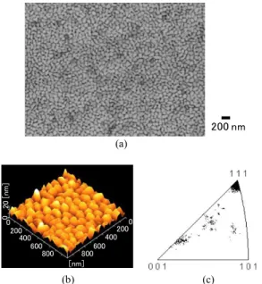
Figure 1 (a) and (b) shows typical SEM and AFM images of the Ti/Au (50 nm/500 nm) film on a Si substrate, re- spectively. The grain structure was clearly observed in the as-deposited film. Figure 1 (c) shows an inverse pole fig- ure obtained from EBSD analysis. The result shows that most of the grains on the as-deposited film have a<111>
orientation. The measured root-mean-square (rms) surface roughness obtained from AFM was 3.6 nm. Most studies of Au-Au SAB using Au films with a surface roughness of a few nanometers showed that a high bonding pressure of 300 MPa was required for the interatomic attraction to over- come surface asperities, and this makes it difficult to achieve Copyright c2017 The Institute of Electronics, Information and Communication Engineers
Fig. 1 Surface morphology and inverse pole figure of Au films prepared by e-beam evaporation with a film thickness of 500 nm. (a) SEM image, (b) AFM image (rms roughness: 3.6 nm), (C) inverse pole figure obtained using EBSD analysis.
Fig. 2 AFM images of Au thin films prepared by e-beam evaporation. (a) Film thickness: 15 nm, rms roughness: 0.24 nm, (b) film thickness: 75 nm, rms roughness: 1.14 nm.
a wafer-scale bonding process without a high bonding pres- sure[7],[12].
The present paper focuses on the use of Au thin films with a film thickness of below 50 nm. To study the depen- dences of the structural and morphological properties on the film thickness, a series of films with an Au thickness of 15 nm∼125 nm were prepared on glass wafers. The rms sur- face roughness of the bare glass wafers was 0.19 nm. Fig- ure 2 shows AFM images of the Ti/Au (3 nm/15 nm) and Ti/Au (3 nm/75 nm) films on the glass substrates. These im- ages clearly show that the grain size increases with the in- crease in the film thickness. Figure 3 shows the rms surface roughness of the Au thin films as a function of the film thick- ness. The surface roughness decreases with the reduction of thickness, and a surface roughness below 0.5 nm was ob- tained when the film thickness was below 50 nm. Surface roughness values below 0.5 nm were smooth enough for di- rect Au-Au bonding.
Fig. 3 Surface roughness of Au thin films as a function of film thickness.
The influence of the Ar plasma treatment on the surface roughness and thickness of the Au thin films was studied.
The rms roughness was 0.42 nm for the Ti/Au (3 nm/30 nm) film on the glass substrate treated with Ar radio frequency (RF) plasma for 30 s (100 W), compared with 0.39 nm for the non-treated sample, indicating that the Ar plasma treat- ment does not significantly deteriorate the surface rough- ness. The change in thickness of the Au thin films between before and after the plasma treatment was typically only a few nanometers from TEM observation.
3. Room-Temperature Wafer Bonding
3.1 Experimental Procedures
Bonding was based on Au-Au SAB at room temperature in ambient air. The bonding procedure is as follows. Prior to bonding, surface activation using Ar radio RF plasma treat- ment (100 W, 30 s) is first carried out to remove organic contamination from the Au surfaces and obtain active sur- faces. Then, the two wafers are brought into contact man- ually within 5 minutes at room temperature in ambient air.
No additional annealing is applied to the samples.
The influence of the air exposure time after Au deposi- tion on the bonding strength in Au-Au bonding was investi- gated. After the Au evaporation, the wafer pairs were stored in air and a particle-free environment (temperature: 20–
25◦C, humidity: 10–15%) for different air exposure times from 10 minutes to 2000 hours. Au-Au bonding with and without Ar RF plasma treatment was performed for com- parison.
After bonding, the bonding strength was measured by a razor blade test (crack-opening method)[15]. In this test, a razor blade is inserted at the interface and the crack length along the bonded interface is observed through the glass wafer. The bonding energyγ[J/m2] (or surface energy) of the bonded pairs, which indicates the bonding strength, is given by
γ= 3
32·ETb2Tw3
L4 (1)
where E(Pa) is the Young’s modulus of the wafer, Tb(m)
Fig. 4 Initiation and self-propagation of bonded area in glass/glass wafer bonding with Ti/Au (3 nm/30 nm) thin films (3 inches in diameter). Bright areas correspond to bonded areas. (a) 0.0 s, (b) 0.2 s, (c) 0.4 s, (d) 0.6 s.
Fig. 5 Bonding energy as a function of the air exposure time after Au deposition[16]. Copyright (2016) The Japan Institute of Electronics Pack- aging
is the blade thickness,Tw(m) is the wafer thickness, andL (m) is the crack length.
Die shear testing for bonding strength measurements was also performed with a die shear tester (Rhesca PTR- 1100). The bonded wafers were diced into chips of 3×3 mm in size for die shear testing.
The microstructure of the bonded interface was ob- served using a TEM system (JEOL JEM-ARM200F).
3.2 Bonding Results
When placing two wafers with the Au sides facing each other, a thin air layer is usually trapped between them, and this prevents immediate spontaneous bonding. Therefore, a light pressure was applied locally on the top wafer to cre- ate the first contact point. In the case of bonding with Ar RF plasma treatment, the bonding front spread immediately after pushing the center of the top wafer, regardless of the long-term air exposure (800 and 2000 h). Figure 4 shows
Fig. 6 Cross-sectional TEM images of Au-Au bonded interface prepared by SAB method at room temperature in ambient air. (a) Low-magnification image, (b) (c) high-magnification image.
a typical example of a bonding front propagation observa- tion. The bonded area expanded across the entire wafer area within 1 s. The bonding process can be simply mon- itored by observing the color change of the wafers owing to the thickness-dependent optical transparency of the Au thin films as the surfaces are brought together. With the excep- tion of the peripheral areas, the entire area was bonded with few voids.
Figure 5 shows experimental results of the bonding en- ergy as a function of the air exposure time after Au depo- sition[16]. The wafers with Ti/Au (3 nm/30 nm) thin films on glass wafers were used for the experiments. The surface
energy of Au is 1.63 J/mm2[17]. In the case of bonding without Ar plasma treatment, the bonding energy decreased with the increasing air exposure time. This result is con- sistent with previously reported results[14]. In the case of an air exposure time of 800 or 2000 hours, the bonded area did not expand by itself across the entire wafer area, and the bonding strength was too low to withstand a dicing process.
On the other hand, the Ar plasma treatment increased the bonding energy significantly.
Bonded wafers with a high bonding energy showed a high die-shear strength (47–70 MPa), and the fractures typi- cally occurred within the bulk of the glass.
Figure 6 shows cross-sectional TEM images of the Au (thickness: 15 nm)–Au (thickness: 15 nm) bonded in- terface with the Ar plasma treatment. The TEM observa- tions showed that even in room temperature bonding in air, a bonded interface at the atomic level was achieved.
Based on these experimental results, the bonding of GaAs and SiC wafers (2 inch in diameter) with Ti/Au (3 nm/
30 nm) films was also successfully achieved at room tem- perature in air. The die shear test showed that the fractures typically occurred within the bulk GaAs rather than at the bonded interface. The wafer-scale GaAs/SiC hetero struc- ture is expected to enable efficient heat dissipation in high- power semiconductor laser applications[18].
4. Conclusions
Room-temperature wafer bonding using smooth Au thin films was demonstrated in air. Without plasma treatment, the bonding strength decreased with the increasing air expo- sure time after Au deposition. Ar RF plasma pretreatment improved the bonding energy significantly, regardless of the air exposure time. The cross-sectional TEM images of the Au–Au bonded interface showed that bonding occurred di- rectly at the atomic level even at room temperature in am- bient air. These results suggest that this technique will be useful for future wafer-scale heterogeneous optoelectronic integration.
Acknowledgments
This work was supported by JSPS KAKENHI Grant Num- ber JP25289085.
References
[1] Z.L. Liau and D.E. Mull, “Wafer fusion: A novel technique for op- toelectronic device fabrication and monolithic integration,” Appl.
Phys. Lett., vol.58, no.8, pp.737–739, 1990.
[2] D. Andrijasevic, M. Austerer, A.M. Andrews, P. Klang, W. Schrenk, and G. Strasser, “Hybrid integration of GaAs quantum cascade lasers with Si substrates by thermocompression bonding,” Appl. Phys.
Lett., vol.92, no.5, 051117, 2008.
[3] E. Higurashi, D. Chino, and T. Suga, “Residue-free solder bump- ing using small AuSn particles by hydrogen radicals,” IEICE Trans.
Electron., vol.E92-C, no.2, pp.247–251, 2009.
[4] E. Higurashi, “Low-Temperature Bonding Technologies for Pho- tonics Applications,” ECS Transactions, vol.50, no.7, Semiconduc-
tor Wafer Bonding 12: Science, Technology, and Applications, pp.351–362, 2012.
[5] T. Suga, Y. Takahashi, H. Takagi, B. Gibbesch, and G. Elssner,
“Structure of Al-Al and Al-Si3N4interfaces bonded at room temper- ature by means of the surface activation method,” Acta Metallurgica et Materialia, vol.40, pp.S133–S137, 1992.
[6] T. Shimatsu, R.H. Mollema, D. Monsma, E.G. Keim, and J.C.
Lodder, “Metal bonding during sputter film deposition,” J. Vac. Sci.
Technol. A, vol.16, no.4, pp.2125–2131, 1998.
[7] E. Higurashi, T. Imamura, T. Suga, and R. Sawada, “Low temper- ature bonding of laser diode chips on Si substrates using plasma activation of Au films,” IEEE Photon. Tech. Lett., vol.19, no.24, pp.1994–1996, 2007.
[8] E. Higurashi, D. Chino, T. Suga, and R. Sawada, “Au-Au Sur- face-Activated Bonding and Its Application to Optical Microsensors with 3-D Structure,” IEEE J. Sel. Topics Quantum Electron., vol.15, no.5, pp.1500–1505, 2009.
[9] R. Takigawa, E. Higurashi, T. Suga, and R. Sawada, “Room-Tem- perature Bonding of Vertical-Cavity Surface-Emitting Laser Chips on Si Substrates Using Au Microbumps in Ambient Air,” Applied Physics Express, vol.1, no.11, 112201, 2008.
[10] T. Sato, E. Higurashi, T. Sato, and R. Sawada, “Low-temperature bonding of laser diode chips using Au stud bumps,” IEICE Trans.
Electron. (Japanese Edition), vol.J94-C, no.11, pp.470–471, Nov.
2011.
[11] E. Higurashi, M. Yamamoto, T. Sato, T. Suga, and R. Sawada,
“Room-temperature gold-gold bonding method based on argon and hydrogen gas mixture atmospheric-pressure plasma treatment for optoelectronic devices integration,” IEICE Trans. Electron., vol.E99-C, no.3, pp.339–345, 2016.
[12] S. Yamamoto, E. Higurashi, T. Suga, and R. Sawada, “Low-tempera- ture hermetic packaging for microsystems using Au-Au surface-acti- vated bonding at atmospheric pressure environment,” J. Micromech.
Microeng., vol.22, no.5, 055026, 2012.
[13] T. Shimatsu, M. Uomoto, K. Oba, and Y. Furukata, “Atomic Diffu- sion Bonding of Wafers in Air with Thin Au Films and Its Applica- tion to Optical Devices Fabrication,” Proc. 2012 3rd IEEE Interna- tional Workshop on Low Temperature Bonding for 3D Integration (LTB-3D), p.103, Tokyo, Japan, May 22-23, 2012.
[14] H. Kon, M. Uomoto, and T. Shimatsu, “Room temperature bonding of wafers using Au films with various holding times in air,” Jour- nal of The Japan Institute of Electronics Packaging, vol.17, no.5, pp.431–435, 2014 (in Japanese).
[15] M.P. Maszara, G. Goetz, A. Cavigila, and J.B. McKitterick, “Bond- ing of silicon wafers for silicon-on-insulator,” J. Appl. Phys., vol.64, no.10, pp.4943–4950, 1988.
[16] Y. Kunimune, K. Okumura, E. Higurashi, T. Suga, and K. Hagiwara,
“Room-temperature wafer bonding using smooth gold thin films for wafer-level MEMS packaging,” 2016 International Conference on Electronics Packaging (ICEP), pp.439–442, Sapporo, Japan, April 20-22, 2016.
[17] L.Z. Mezey and J. Giber, “The Surface Free Energies of Solid Chem- ical Elements: Calculation from Internal Free Enthalpies of Atom- ization,” Jpn. J. Appl. Phys., vol.21, pp.1569–1571, 1982.
[18] E. Higurashi, K. Okumura, K. Nakasuji, and T. Suga, “Surface activated bonding of GaAs and SiC wafers at room temperature for improved heat dissipation in high-power semiconductor lasers,”
Japanese Journal of Applied Physics, vol.54, no.3, 030207, 2015.
Eiji Higurashi received the M.E. and Ph.D.
degrees from Tohoku University, Sendai, Japan, in 1991 and 1999, respectively. He was with Ni- ppon Telegraph and Telephone Corporation, To- kyo, Japan, from 1991 to 2003, where he was engaged in the field of laser manipulation and optical microsensors. He was an associate pro- fessor in the Research Center for Advanced Sci- ence and Technology (RCAST) at the University of Tokyo from 2004 to 2014 and has been an as- sociate professor in the Department of Precision Engineering at the University of Tokyo since 2003. His current research interests include low-temperature bonding methods and the integration and packaging technology for optical microsystems.
Ken Okumura received the B.S. and M.S. degrees from University of Tokyo, Tokyo, Japan, in 2014 and 2016, respectively. During a master course, he was engaged in research on room temperature bonding methods. He is now with Central Japan Railway Company.
Yutaka Kunimune received B.E. degree from Waseda University, Tokyo, Japan, in 2015.
He is currently working toward the M.E. degree at The University of Tokyo, Tokyo, Japan. His current research interests include Au-Au surface activated bonding.
Tadatomo Suga joined the Max-Planck In- stitut f¨ur Metallforschung in 1979, obtained his Ph.D. degree in materials science from Univer- sity of Stuttgart in 1983. Since 1984 he has been a faculty member of the University of To- kyo, and has been a professor in the Department of Precision Engineering of the School of En- gineering since 1993. He was also the director of the Research Group of Interconnect Ecode- sign at the National Institute of Materials Sci- ence (NIMS), a Member of the Japan Council of Science, the Chair of IEEE CPMT Society Japan Chapter, and the Pres- ident of the Japan Institute for Electronic Packaging. His research focuses on microelectronics and microsystems packaging, and development of key technologies related to low temperature bonding and interconnects as well as disassembly concept for EcoDesign.
Kei Hagiwara received the B.S. degree in image science from Chiba University, Chiba, Japan, in 1995, and the Ph.D. degree in me- chanical engineering from the University of To- kyo, Tokyo, Japan, in 2015. He joined the Japan Broadcasting Corporation (NHK), Tokyo, Japan, in 1995, where he has been with the Science and Technology Research Laborato- ries, since 1998. His current research interests include wafer-bonding and layer-transfer tech- nologies, and 3-D integrated CMOS-MEMS de- vices.
![Fig. 5 Bonding energy as a function of the air exposure time after Au deposition[16]. Copyright (2016) The Japan Institute of Electronics Pack-aging](https://thumb-ap.123doks.com/thumbv2/123deta/5624255.1500010/3.892.107.394.108.430/bonding-energy-function-exposure-deposition-copyright-institute-electronics.webp)
