INVITED PAPER
Special Section on Progress towards System NanotechnologyRoom-Temperature Gold-Gold Bonding Method Based on Argon and Hydrogen Gas Mixture Atmospheric-Pressure Plasma
Treatment for Optoelectronic Device Integration
Eiji HIGURASHI†a),Member, Michitaka YAMAMOTO†, Takeshi SATO†, Tadatomo SUGA†, andRenshi SAWADA††,Nonmembers
SUMMARY Low-temperature bonding methods of optoelectronic chips, such as laser diodes (LD) and photodiode (PD) chips, have been the focus of much interest to develop highly functional and compact opto- electronic devices, such as microsensors and communication modules. In this paper, room-temperature bonding of the optoelectronic chips with Au thin film to coined Au stud bumps with smooth surfaces (Ra: 1.3 nm) using argon and hydrogen gas mixture atmospheric-pressure plasma was demon- strated in ambient air. The die-shear strength was high enough to exceed the strength requirement of MIL-STD-883F, method 2019 (×2). The mea- sured results of the light-current-voltage characteristics of the LD chips and the dark current-voltage characteristics of the PD chips indicated no degra- dation after bonding.
key words: heterogeneous integration, low-temperature bonding, surface- activated bonding, atmospheric-pressure plasma, optical microsystems
1. Introduction
Heterogeneous integration of materially different optical components made with wide ranges of fabrication processes onto a single platform enables us to construct small, high- performance, and multifunctional optoelectronic devices.
Low-temperature bonding methods are important integra- tion techniques for realizing advanced optoelectronic de- vices[1]. Table 1 summarizes typical bonding techniques used for semiconductor device fabrication. Bonding meth- ods are categorized into two groups: direct bonding, such as anodic bonding and fusion bonding, and intermediate layer bonding, such as solder bonding, thermocompression bond- ing, and adhesive bonding. All these methods have emerged in response to many different applications. Among these bonding methods, low-temperature bonding methods have been the focus of recent interest to create unique device structures for a wide range of photonic applications. The ad- vantage of low-temperature bonding methods is that they are free from the various problems caused by the large thermal expansion mismatch between the bonding materials during annealing in the conventional bonding methods.
Here, we focus on intermediate layer bonding using gold (Au). Au has several highly desirable properties, such
Manuscript received August 5, 2015.
Manuscript revised November 20, 2015.
†The authors are with The University of Tokyo, Tokyo, 113–
8656 Japan.
††The author is with Kyushu University, Fukuoka-shi, 819–
0395 Japan.
a) E-mail: [email protected] DOI: 10.1587/transele.E99.C.339
as oxidation and corrosion resistance, as well as high electri- cal and thermal conductivities. Due to these properties, Au has been typically used as the top layer metal of the elec- trodes of many optoelectronic devices. Recently, numerous experimental studies on low-temperature Au-Au bonding have been carried out[2]–[16]. Surface-activated bonding (SAB) is one of the most promising candidates for achieving low-temperature metal bonding. Au-Au SAB enables bond- ing at low-temperature (from room temperature to 150◦C) in ambient air. The SAB of a laser diode (LD) with Au thin films to Au thin film[4], to Au microbumps[6], or to coined Au stud bumps[8]has been reported using low-pressure ar- gon (Ar) radio frequency plasma. Three-dimensional (3D) integration of multiple chips has been demonstrated due to its characteristics of low-temperature solid-state bonding for high-density packaging. However, the low-pressure plasma process requires an expensive vacuum system and has the problem of increased process time for the vacuum process- ing.
In this paper, to realize a low-cost instrument and to improve productivity, atmospheric-pressure (AP) plasma, which has been successfully applied for a pretreatment method for ultrasonic bonding[17],[18], is applied to Au- Au SAB. The entire bonding process, including surface ac- tivation, is carried out in ambient air. In addition, to realize room-temperature bonding, thick Au bumps (>10µm) with smooth surfaces (Ra < 3 nm) fabricated by a simple stud bumping and coining process are used for bonding.
2. Experiments
2.1 Bump Fabrication and Bonding Processes
Au bump fabrication and low-temperature bonding pro- cesses are shown in Fig. 1. Au stud bumps are formed on silicon (Si) substrates by a stud bonding machine [Fig. 1 (a)].
They can be easily formed on the 3-D structure sub- strate, because the fabrication process does not require pho- tolithography. However, typical stud bumps have sharp tips on top of the bumps. If the LD chip is bonded on stud bumps with sharp tips, stress concentration will lead to its degrada- tion. Therefore, a coining process using the flat surface of the Si chips was used to flatten the tips and create smooth tops of the stud bumps. The tips of the Au stud bumps are Copyright c2016 The Institute of Electronics, Information and Communication Engineers
Table 1 Typical bonding techniques used for semiconductor device fabrication.
Fig. 1 Schematic diagram of the bump fabrication and bonding pro- cesses: (a) Au stud bumping, (b) coining using Si chip, (c) formation of a flat and smooth top surface, (d) atmospheric-pressure plasma treatment, (e) low-temperature bonding in ambient air.
coined by being pressed against the flat surface of the Si chip [Figs. 1 (b), (c)]. Then, the Au bumps on the Si substrate and the Au thin film on the chips are activated by AP plasma [Fig. 1 (d)]. After plasma activation, the Au bumps and Au thin film are brought into contact for 30 s with a controlled contact load and temperature in ambient air [Fig. 1 (e)].
2.2 Experimental Procedure
AP plasma based on a dielectric barrier discharge was used for the surface activation of Au prior to low-temperature Au- Au bonding. The plasma treatment was performed with two different mixed gases: argon-oxygen mixed gas (Ar+O2) and argon-hydrogen mixed gas (Ar+H2). An AP plasma processing unit (Aiplasma, Matsushita Electric Works Co.) was used for the experiments. The conditions of the AP plasma treatment are shown in Table 2.
For investigation of the AP plasma containing active species, optical emission spectroscopy was performed using a multiband plasma-process monitor (Hamamatsu Photon- ics, C10346-01).
Bonding strength was evaluated by using Si chips (width: 300µm, length: 300µm, height: 100µm) with Au thin films (thickness: 0.5µm, Ra: 1.3 nm) instead of real LD chips. The bumps array arrangement for the bonding
Table 2 Atmospheric-pressure plasma treatment conditions.
Fig. 2 Schematic diagram of the arrangement of bump arrays: (a) for die-shear test chips, (b) for LD chips.
of Si chips is shown in Fig. 2 (a). Au stud bumps (purity:
99.99%) coined at 450 gf (28 gf/bump) were used for the ex- periments. Bonding strength was tested by the shear tester (RHESCA PTR-1100). The fracture mode was analyzed with scanning electron microscopy (SEM) after the die shear test.
InGaAsP/InP buried heterostructure LD chips (width:
400µm, length: 450µm, height: 100µm, wavelength:
1.31µm) with Au thin film electrodes (thickness: 0.5µm, Ra: 2.1 nm) were used to evaluate the optoelectronic charac- teristics before and after bonding. The bumps array arrange- ment for the bonding of LD chips is shown in Fig. 2 (b). An active region of the buried heterostructure LD chip is buried in the lower refractive indices InP layers on all sides. The bumps were located away from the active region to reduce the stress in the active region, as described later.
Surface-illuminated and flip-chip-mountable InGaAs
PD chips (width: 280µm, length: 460µm, thickness:
150µm), which have the anode and cathode (pad diameter:
80µm) on the same side, were used to investigate the influ- ence of AP plasma treatment on the electric properties of PD chips. The electrode pads of a PD chip have a metallization consisting of 1µm of Au.
Light-current-voltage (L-I-V) characteristics of LD chips and dark current-voltage (I-V) characteristics of PD chips were measured by an L-I-V test system (Asahi Data Systems, ALT-7103B) and an electrometer (Keithley Model 6517A), respectively.
3. Numerical Analysis of Stress Distribution during Compressive Loading
To determine the arrangement of bump arrays, the stress distribution in the active region of the buried heterostruc- ture LD chip was analyzed based on the 3D elastic-plastic finite element method. It is known that large stress on an LD chip generates dislocations in the active region and leads to degradations. Therefore, it is required to reduce the stress caused by the compressive loading. Figure 3 shows the three-dimensional analysis model. For compar- ison, we prepared two models: InP LD chips with Au thin films (thickness: 0.5µm) to Au thin film (thickness: 0.5µm) [Fig. 3 (a)] and to Au stud bumps (45µm square and 10µm thick) [Fig. 3 (b)]. The location of the active region is 5µm from the bottom surface of the LD chip (junction-down con- figuration). The bumps were located away from the active region to reduce the stress in the active region.
Figure 4 shows the simulated cross-sectional profile of the von Mises stress distribution in the LD chip when the bonding pressure of 52 MPa was applied on top of the chip
Fig. 3 Schematic diagram of the three-dimensional analysis models:
(a) an InP LD chip on Au thin film, (b) an InP LD chip on Au bumps.
Fig. 4 Simulated cross-sectional profile of the von Mises stress distribu- tion in an InP LD chip when a bonding pressure of 52 MPa was applied on top of the chip: (a) Au thin film, (b) Au bumps.
(no change in temperature). Because there is an axis of sym- metry at the center of the LD chip, only one-half of the cross-section is shown. The results show that appropriate arrangement of bump arrays can reduce the stress in the ac- tive layer of the LD chip to a value as low as 20 MPa. Al- ternately, the LD chip on the Au thin film generated a large stress over 100 MPa at the edge of the active region. It has been reported that stress as small as 20 MPa does not affect the characteristics of quantum well structures[19].
4. Experimental Results and Discussion
4.1 Coined Stud Bumps
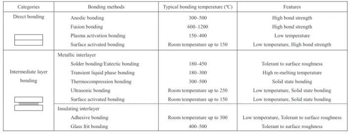
Coined Au stud bumps (purity: 99.99%) were fabricated us- ing Si chips (Ra: 0.2 nm). Typical SEM images of Au stud bumps before and after coining are shown in Fig. 5. The surface area increased and the height of the Au stud bumps decreased with increasing coining load (Table 3). Figure 6 shows a typical atomic force microscope (AFM) image of the top of a coined bump (28 gf/bump). Thick Au bumps (thickness: 15.3µm) with smooth surfaces (Ra: 1.3 nm) were realized on the Si substrate. These bumps are easily fabri- cated at the bottom of the cavity structures.
4.2 Optical Emission Spectroscopy
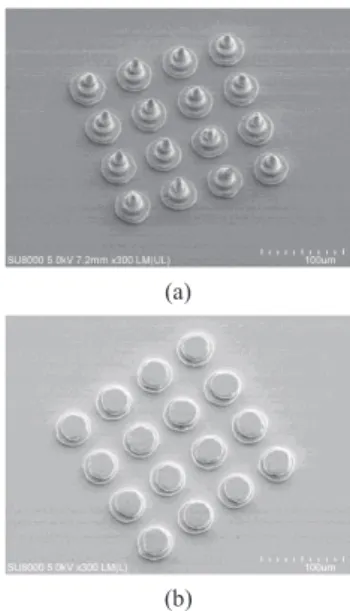
Typical emission spectra are shown in Fig. 7. The observed
Fig. 5 SEM images of Au stud bumps: (a) before coining, (b) after coining (coining load: 28 gf/bump).
Table 3 Relationship between the coining load, surface area, and height of Au stud bumps.
Fig. 6 AFM image of the top surface of an Au stud bump after coining (coining load: 28 gf/bump).
Fig. 7 Measured emission spectra: (a) Ar+O2AP plasma, (b) Ar+H2
AP plasma.
emission spectrum of Ar+O2AP plasma [Fig. 7 (a)] is dom- inated by bands of O (maximum at 777 nm) and Ar (maxi- mum at 811 nm). The atomic oxygen (O) can react with car- bon containing contamination on the Au surface to form gas phase products such as CO and CO2. Alternately, Ar+H2
AP plasma radiation [Fig. 7 (b)] contains the emission of NO (maximum at 236 nm), OH (maximum at 309 nm), NH (maximum at 336 nm) and Ar (maximum at 811 nm). The NO (NOγ-system) is from the water vapor in the air and is known to react with ozone (O3) and produce atomic oxygen (O)[20]. Therefore, highly reactive hydroxyl (OH) and O react with organic contaminants on the Au surface to form
Fig. 8 Typical cross-sectional SEM image of a bonded LD chip on the Si substrate.
Fig. 9 Die-shear strength with different gases and bonding temperatures (contact load: 680 gf).
gas-phase products.
The plasma-treated surfaces were characterized by X- ray photoelectron spectroscopy (XPS) analysis. The mea- sured C1s region was mainly composed of C-C bonds (284.5 eV)[21] and C-H bonds (285.4 eV)[21] before plasma treatment, and the C1s peak was significantly de- creased after the AP plasma treatment (30 s).
4.3 Bonding Strength
Figure 8 shows a typical SEM image of the cross section of a bonded LD chip on the Si substrate. Figure 9 shows the effect of the bonding temperature (25 and 150◦C) on the die-shear strength (contact load: 680 gf) of the Si chips. The shear strength failure criteria from MIL-STD-883F, method 2019 (×2), for the used chips (width: 300µm, length:
300µm) is 112 gf. The die-shear strength increased with in- creasing bonding temperature, and Ar+H2AP plasma treat- ment improved the die-shear strength significantly. Even at a bonding temperature of 25◦C, the die-shear strength ex- ceeded the failure criteria. However, with Ar+O2 plasma treatment, the die-shear strength did not exceed the failure criteria.
After the treatment of Ar+O2plasma, oxidation of the Au surface (Au2O3) was detected by the chemical shift of the 4f levels in XPS spectra[22],[23]. Although Au is most resistant against oxidation in air, even at high temperatures, the plasma oxidation of Au samples has been reported in the
Fig. 10 SEM images of fractured surfaces after the die-shear test (left:
substrate side, right: chip side): (a) Ar+O2AP plasma treatment, (b) Ar+H2
AP plasma treatment.
literature[18],[24],[25]. It has also been reported that the gold oxide thermally desorbs in two steps (170 and 260◦C) and that an annealing temperature of over 260◦C is neces- sary for the oxide removal[25]. The surface oxide layers impede bonding between Au and Au. Therefore, the need for oxide-free Au surfaces prior to Au-Au bonding is criti- cal for low-temperature bonding. In the case of Ar+H2AP plasma treatment, hydrogen radicals may remove the gold oxide.
SEM images of the fractured surfaces after the die- shear test are shown in Fig. 10. In the case of Ar+H2
AP plasma treatment, Au bumps were transferred to the chip side, as shown in Fig. 10 (b). This also indicates that Ar+H2 AP plasma treatment realizes strong bonding be- tween Au/Au surfaces.
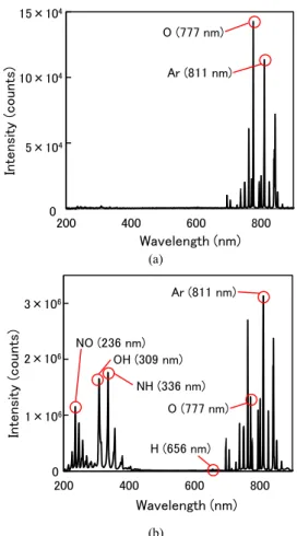
4.4 Electro-Optical Characteristics of LD and PD Chips InGaAsP/InP LD chips and InGaAs PIN PD chips were bonded with coined Au stud bumps (bonding temperature:
150◦C). Figure 11 shows the typical light-current-voltage characteristics of the LD chips and the dark current-voltage characteristics of the PD chips before and after bonding us- ing Ar+H2AP plasma treatment. These results indicated no degradation after bonding.
5. Conclusions
Room temperature bonding of the optoelectronic chips in ambient air was demonstrated using Au-Au SAB based on AP plasma treatment. Ar+H2AP plasma treatment was ef- fective in improving the bondability between Au/Au sur- faces compared with Ar+O2 AP plasma treatment. It has the advantage of being low-cost because an expensive vac- uum chamber and pump for evacuation are not required for plasma generation. This Au-Au SAB method is expected to
Fig. 11 Typical electro-optical characteristics of LD and PD chips before and after bonding using Ar+H2AP plasma treatment: (a) L-I-V character- istics, (b) Dark I-V characteristics.
be a useful technique for future optoelectronic device inte- gration.
Acknowledgments
Part of this study was supported by JSPS KAKENHI Grant Numbers 23246125 and 25289085.
References
[1] E. Higurashi, “Low-temperature bonding technologies for photonics applications”, ECS Transactions, vol.50, no.7, Semiconductor Wafer Bonding 12: Science, Technology, and Applications, pp.351–362, 2012.
[2] M.M.V. Taklo, P. Storås, K. Schjølberg-Henriksen, H.K. Hasting, and H. Jakobsen, “Strong, high-yield and low-temperature thermo- compression silicon wafer-level bonding with gold,” J. Micromech.
Microeng., vol.14, no.7, pp.884–890, 2004.
[3] Q.-Y. Tong, “Room temperature metal direct bonding,” Appl. Phys.
Lett., vol.89, 182101, 2006.
[4] E. Higurashi, T. Imamura, T. Suga, and R. Sawada, “Low- temperature bonding of laser diode chips on Silicon substrates using plasma activation of Au films,” IEEE Photon. Tech. Lett., vol.19, no.24, pp.1994–1996, 2007.
[5] X.F. Ang, Z. Chen, C.C. Wong, and J. Wei, “Effect of chain length on low temperature gold-gold bonding by self-assembled monolayers,”
Appl. Phys. Lett., vol.92, 131913, 2008.
[6] R. Takigawa, E. Higurashi, T. Suga, and R. Sawada, “Room- temperature bonding of vertical-cavity surface-emitting laser chips
on Si substrates using Au Microbumps in ambient air,” Applied Physics Express, vol.1, no.11, 112201, 2008.
[7] E. Higurashi, D. Chino, T. Suga, and R. Sawada, “Au-Au surface- activated bonding and its application to optical microsensors with 3-D structure,” IEEE J. Sel. Topics Quantum Electron., vol.15, no.5, pp.1500–1505, 2009.
[8] T. Sato, E. Higurashi, T. Suga, and R. Sawada, “Low-temperature bonding of laser diode chips using Au stud bumps,” IEICE Trans.
Electron. (Japanese edition), vol.J94-C, no.11, pp.470–471, 2011.
[9] T. Shimatsu, M. Uomoto, K. Oba, and Y. Furukata, “Atomic dif- fusion bonding of wafers in air with thin Au films and its applica- tion to optical devices fabrication,” Proc. 2012 3rd IEEE Interna- tional Workshop on Low Temperature Bonding for 3D Integration (LTB-3D), p.103, Tokyo, Japan, 2012.
[10] H. Oppermann and L. Dietrich, “Nanoporous gold bumps for low temperature bonding,” Microelectronics Reliability, vol.52, no.2, pp.356–360, 2012.
[11] H. Ishida, T. Ogashiwa, Y. Kanehira, H. Murai, T. Yazaki, S.
Ito, and J. Mizuno, “Surface compliant bonding properties of low- temperature wafer bonding using sub-micron Au particles,” 2013 IEEE 63rd Electronic Components and Technology Conference (ECTC), pp.1519–1523, 2013.
[12] A. Okada, S. Shoji, M. Nimura, A. Shigetou, K. Sakuma, and J. Mizuno, “Vacuum ultraviolet irradiation treatment for reduc- ing gold-gold bonding temperature,” Materials Transactions, vol.54, no.11, pp.2139–2143, 2013.
[13] A. Rantam¨aki, J. Lindfors, M. Silvennoinen, J. Kontio, M. Tavast, and O.G. Okhotnikov, “Low temperature gold-to-gold bonded semi- conductor disk laser,” IEEE Photon. Tech. Lett., vol.25, no.11, pp.1062–1065, 2013.
[14] Y. Kurashima, A. Maeda, R. Takigawa, and H. Takagi, “Room tem- perature wafer bonding of metal films using flattening by thermal imprint process,” Microelectronic Engineering, vol.112, pp.52–56, 2013.
[15] K. Okumura, E. Higurashi, T. Suga, and K. Hagiwara, “Room- temperature wafer bonding with smooth Au thin film in ambient air using Ar RF plasma activation,” Proc. 2014 4th IEEE Interna- tional Workshop on Low Temperature Bonding for 3D Integration (LTB-3D), p.26, Tokyo, Japan, 2014.
[16] W.-S. Wang, Y.-C. Lin, T. Gessner, and M. Esashi, “Fabrication of nanoporous gold and the application for substrate bonding at low temperature,” Jpn. J. Appl. Phys., vol.54, no.3, 030215, 2015.
[17] J.-M. Koo, J.-L. Jo, J.-B. Lee, Y.-N. Kim, J.-W. Kim, B.-I. Noh, J.-H. Moon, D.-U. Kim, and S.-B. Jung, “Effect of atmospheric pressure plasma treatment on transverse ultrasonic bonding of gold flip-chip bump on glass substrate,” Jpn. J. Appl. Phys., vol.47, no.5S, pp.4309–4313, 2008.
[18] J.-M. Koo, J.-B. Lee, Y.J. Moon, W.-C. Moon, and S.-B. Jung, “At- mospheric pressure plasma cleaning of gold flip chip bump for ul- trasonic flip chip bonding,” Journal of Physics: Conference Series, vol.100, 012034, 2008.
[19] S. Zankovych, I. Maximov, I. Shorubalko, J. Seekamp, M. Beck, S. Romanov, D. Reuter, P. Schafmeister, A.D. Wieck, J. Ahopelto, C.M.S. Torres, and L. Montelius, “Nanoimprint-induced effects on electrical and optical properties of quantum well structures,” Micro- electronic Engineering, vol.67, no.68, pp.214–220, 2003.
[20] M. Griggs, “Absorption coefficients of ozone in the ultraviolet and visible regions,” Journal of Chemical Physics, vol.49, no.2, pp.857–859, 1968.
[21] A.-M.B. Al-Ajlony, A. Kanjilal, S.S. Harilal, and A. Hassanein,
“Carbon contamination and oxidation of Au surfaces under extreme ultraviolet radiation: An x-ray photoelectron spectroscopy study,”
Journal of Vacuum Science & Technology B, vol.30, no.4, 041603, 2012.
[22] R. Takigawa, E. Higurashi, T. Suga, and R. Sawada, “Low- temperature bonding of laser diode chips on Si substrates with oxy- gen and hydrogen atmospheric-pressure plasma activation,” 2009 In-
ternational Conference on Electronic Packaging Technology & High Density Packaging (ICEPT-HDP), pp.475–477, Beijing, China, 2009.
[23] S. Matsuoka, M. Yamamoto, E. Higurashi, T. Suga, and R. Sawada,
“Low temperature Au-Au surface-activated bonding using nitro- gen atmospheric-pressure plasma treatment for optical microsys- tems,” 2015 International Conference on Electronics Packaging
& iMAPS All Asia Conference (ICEP-IAAC 2015), pp.850–853, Kyoto, Japan, 2015.
[24] H. Tsai, E. Hu, K. Perng, M. Chen, J.-C. Wu, and Y.-S. Chang,
“Instability of gold oxide Au2O3,” Surf. Sci. Letters, vol.537, pp.L447–L450, 2003.
[25] T. Sakata, Y. Okabe, K. Kuwabara, N. Sato, K. Ono, N. Shimoyama, K. Machida, and H. Ishii, “Surface cleaning of gold structure by annealing during fabrication of microelectromechanical system de- vices,” Jpn. J. Appl. Phys., vol.48, no.2R, 026501, 2009.
Eiji Higurashi received the M.E. and Ph.D.
degrees from Tohoku University, Sendai, Japan, in 1991 and 1999, respectively. He was with Nippon Telegraph and Telephone Corporation, Tokyo, Japan, from 1991 to 2003, where he was engaged in the field of laser manipulation and optical microsensors. He was an associate pro- fessor in the Research Center for Advanced Sci- ence and Technology (RCAST) at the University of Tokyo from 2004 to 2014 and has been an as- sociate professor in the Department of Precision Engineering at the University of Tokyo since 2003. His current research interests include low-temperature bonding methods and the integration and packaging of optical microsystems.
Michitaka Yamamoto received the B.S. and M.S. degrees from University of Tokyo, Tokyo, Japan, in 2012 and 2014, respectively. During a master course student, he was engaged in re- search on low temperature bonding methods. He is now with Kyocera corporation.
Takeshi Sato received the B.S. and M.S.
degrees from the University of Tokyo, Japan, in 2010 and 2012, respectively. During a mas- ter course, he was engaged in research on low- temperature bonding technology with Surface Activation. He is now with Hitachi, Ltd.
Tadatomo Suga joined the Max-Planck In- stitut f¨ur Metallforschung in 1979, obtained his Ph.D. degree in materials science from Univer- sity of Stuttgart in 1983. Since 1984 he has been a faculty member of the University of Tokyo, and has been a professor in the Department of Precision Engineering of the School of Engi- neering since 1993. He was also the director of the Research Group of Interconnect Ecode- sign at the National Institute of Materials Sci- ence (NIMS), a Member of the Japan Council of Science, the Chair of IEEE CPMT Society Japan Chapter, and the Pres- ident of the Japan Institute for Electronic Packaging. His research focuses on microelectronics and microsystems packaging, and development of key technologies related to low temperature bonding and interconnects as well as disassembly concept for EcoDesign.
Renshi Sawada received the B.E., M.E., and Ph.D. degrees from Kyushu University, Fukuoka, Japan, in 1976, 1978, and 1995, re- spectively. In 1978, he joined the Electri- cal Communication Laboratories, Nippon Tele- graph and Telephone, Tokyo. Since January 2004, he has been at Kyushu University, Fuku- oka, Japan, where he was engaged in the re- search on the polishing of Si substrates, getter- ing of Si crystalline defects, fabrication of di- electrically isolated Si substrates (silicon on in- sulator substrate process), and optical microelectromechanical systems, such as micromirror array, integrated optical displacement sensors, MEMS shearing sensor and MEMS slip sensor, MEMS integrated optical blood flow sensor, integrated scanning microscope, and sensors attachable to an- imals and humans for network.