INVITED PAPER
Special Section on Fabrication Technologies Supporting the Photonic/Nanostructure DevicesSurface Emitting Devices Based on a Semiconductor Coupled
Multilayer Cavity for Novel Terahertz Light Sources
Takahiro KITADA†a), Hiroto OTA†, Xiangmeng LU†, Naoto KUMAGAI†∗, and Toshiro ISU†, Nonmembers
SUMMARY Compact and room-temperature operable terahertz emit-ting devices have been proposed using a semiconductor coupled multilayer cavity that consists of two functional cavity layers and three distributed Bragg reflector (DBR) multilayers. Two cavity modes with an optical fre-quency difference in the terahertz region are realized since two cavities are coupled by the intermediate DBR multilayer. In the proposed device, one cavity is used as the active layer for two-color lasing in the near-infrared re-gion by current injection and the other is used as the second-order nonlinear optical medium for difference-frequency generation of the two-color funda-mental laser light. The control of the nonlinear polarization by face-to-face bonding of two epitaxial wafers with different orientations is quite effec-tive to achieve bright terahertz emission from the coupled cavity. In this study, two-color emission by optical excitation was measured for the wafer-bonded GaAs/AlGaAs coupled multilayer cavity containing self-assembled InAs quantum dots (QDs). We found that optical loss at the bonding inter-face strongly affects the two-color emission characteristics when the bond-ing was performed in the middle of the intermediate DBR multilayer. The effect was almost eliminated when the bonding position was carefully cho-sen by considering electric field distributions of the two modes. We also fabricated the current-injection type devices using the wafer-bonded cou-pled multilayer cavities. An assemble of self-assembled QDs is considered to be desirable as the optical gain medium because of the discrete nature of the electronic states and the relatively wide gain spectrum due to the inhomogeneous size distribution. The gain was, however, insufficient for two-color lasing even when the nine QD layers were used. Substituting two types of InGaAs multiple quantum wells (MQWs) for the QDs, we were able to demonstrate two-color lasing of the device when the gain peaks of MQWs were tuned to the cavity modes by lowering the operating tempera-ture.
key words: coupled multilayer cavity, two-color lasing, frequency
conver-sion, terahertz source 1. Introduction
Useful terahertz light sources have been extensively in-vestigated because of the wide range of possible appli-cations including wireless communication, spectroscopy, and imaging[1],[2]. Recent femtosecond laser technolo-gies have it made possible to generate ultrashort terahertz pulses covering extremely broad bandwidth[3]–[5]. Sev-eral types of semiconductor-based devices such as quantum cascade lasers (QCLs)[6]–[8], resonant tunneling diodes (RTDs)[9],[10], and photomixers[11],[12]have also been studied and developed for continuous-wave (cw) terahertz
Manuscript received June 10, 2016. Manuscript revised September 19, 2016.
†The authors are with the Graduate School of Science and
Technology, Tokushima University, Tokushima-shi, 770–8506 Japan.
∗Presently, with the National Institute of Advanced Industrial
Science and Technology (AIST). a) E-mail: [email protected]
DOI: 10.1587/transele.E100.C.171
emitter. Terahertz sources based on intracavity difference-frequency generation (DFG) in dual wavelength mid-infrared QCLs have also been recently reported[13],[14]. However, there are still challenges associated with each of these devices. For instance, the emission power becomes insufficient for higher frequency operation of RTDs. In ad-dition, although significant progress has been made on tera-hertz QCLs, near-room-temperature operation has not been demonstrated.
Optical microcavities are good candidates for nonlin-ear optical devices because an extremely strong electric field is realized in the cavity layer sandwiched between two dis-tributed Bragg reflector (DBR) multilayers. Efficient wave-length conversion is possible in the GaAs-based multilayer cavity when the structure is grown on a non-(001) substrate to allow the second-order nonlinearity of zincblende-type semiconductors[15]. In fact, blue vertical-cavity surface emitting lasers (VCSELs) have been demonstrated utilizing second-harmonic generation (SHG) on (113)B and (114)A GaAs substrates[16]. Recently, we have proposed a GaAs/
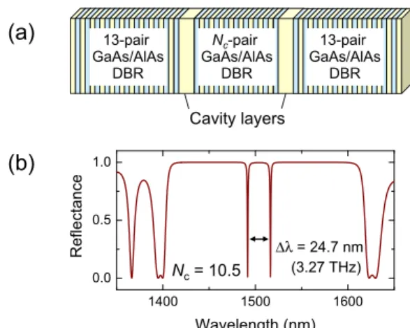
AlAs coupled multilayer cavity structure for novel terahertz emitting devices[17]. An example of the structure is shown in Fig. 1 (a). The structure consists of two equivalent cavity layers and three DBR multilayers. As shown in the sim-ulated optical reflection spectrum of Fig. 1 (b), two cavity modes appear in the center of the high reflection band. This is because a degenerate cavity mode is split into two dif-ferent modes as a result of coupling of the cavity layers. Note that the mode frequency difference can be precisely
Fig. 1 (a) An example of GaAs-based coupled multilayer cavity structure and (b) its reflection spectrum.
defined within the terahertz region according to the number (Nc) of pairs of the intermediate DBR. The electric field of
each mode is greatly enhanced in both cavity layer, allow-ing strong frequency-mixed signal to be generated. Since the effective second-order nonlinear coefficient is zero on a (001)-oriented GaAs substrate due to crystal symmetry[15], a non-(001) substrate is essential for crystal growth. We have obtained a strong sum-frequency generation (SFG) sig-nal from a GaAs/AlAs coupled multilayer cavity grown on a (113)B GaAs substrate when the two modes were si-multaneously excited by 100 fs laser pulses[18]–[20]. The peak intensity of the SFG signal was more than 400 times greater than that of the SHG from the (113)B GaAs bulk substrate. DFG signals from the (113)B coupled cavity sam-ples were also demonstrated at room temperature by time-resolved waveform measurements using 100 fs laser pulses and a photoconductive antenna[21]–[23]. In addition, we found that polarization control is necessary to obtain a large terahertz DFG signal from two modes[24],[25].
From the view point of practical device applications, the two modes should be generated inside the structure by current injection, since this enables terahertz emission through DFG without external light sources. We have al-ready demonstrated the two mode emission by optical exci-tation using self-assembled InAs quantum dots (QDs) that were inserted only in the one cavity layer to realize opti-cal gain in the near-infrared region[26]–[28]. In this pa-per, we report recent progress on design and fabrication technologies of the GaAs-based coupled multilayer cav-ity toward compact and room-temperature operable tera-hertz light emitting devices. We also fabricated the current-injection type devices using the coupled cavity wafers and demonstrated two-color lasing of the device in the near-infrared region.
2. Polarization Control for Efficient DFG
Let us consider nonlinear polarization P for DFG of two modes in the terahertz frequency region. According to the second-order nonlinear process, the polarization is ex-pressed by the relation P = χ(2)E∗
1E2, where χ(2) is the
second-order nonlinear susceptibility, and E1and E2are the
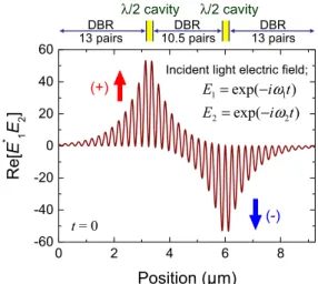
electric fields of the two modes inside the structure. Fig-ure 2 shows a spatial distribution of E1∗E2simulated for the
GaAs/AlAs coupled multilayer cavity at a given time. Ef-ficient DFG of the two modes might be expected since the amplitude of E∗1E2 is greatly enhanced in the cavity layer
regions. Note that the sign of E∗1E2 changes from positive
to negative moving from one side of the cavity to the other. As the time proceeds, the intensity oscillates with a period of the mode frequency difference while keeping the oppo-site signs of E1∗E2. The distance L between the two
cav-ity layers is much smaller than half the DFG wavelength λ/2nTHz, where nTHzis the refractive index of GaAs at the
corresponding terahertz frequency. For the structure shown in Fig. 2, L∼ 2.54 μm and λ/2nTHz∼ 12.6 μm. The radiated
terahertz fields from the two cavity layers, therefore, largely
Fig. 2 Spatial distribution of E∗1E2simulated for the GaAs/AlAs
coupled multilayer cavity.
cancel each other out due to the phase mismatch when both cavity layers have the sameχ(2). The cancellation could be significantly eliminated using the different χ(2)for each
cav-ity layer. In the normal incidence configuration, an effec-tiveχ(2) is nonzero on a high-index substrate and strongly
depends on the substrate orientation[15]. Note that a 180◦ rotation of the crystal around the appropriate axis inverts the sign of χ(2) on the (11n)-oriented substrate. Thus, the different χ(2) for each cavity is enabled by the face-to-face
connection of the two halves of the coupled cavity struc-ture grown on substrates with the same or different crystal orientations. We have already demonstrated significant en-hancement of the DFG signal by theχ(2)inversion. The
in-verted coupled cavity sample was fabricated by direct wafer bonding of two (113)B epitaxial wafers and the enhance-ment was confirmed through the comparison of inverted and normal coupled cavity samples in both simulated and exper-imentally observed terahertz waveforms produced by fem-tosecond laser pulses[25].
3. Coupled Multilayer Cavity
3.1 Design and Fabrication
An ensemble of self-assembled InAs QDs is a good can-didate for the optical gain medium because the gain spec-trum is broadened sufficiently such that it covers both cavity modes due to the size inhomogeneity, whereas the individ-ual QDs have discrete electronic states. Bright emission is typically observed from the InAs QDs on the (001) GaAs substrates. However, DFG through a second-order nonlin-ear process is forbidden on the (001) substrate due to crys-tal symmetry, that is,χ(2) = 0. The (113)B GaAs substrate
gives relatively largeχ(2)among high-index substrates while
keeping good crystalline quality of the epitaxially grown GaAs/AlGaAs multilayer structure. In our study, two epi-wafers were prepared by molecular beam epitaxy (MBE) on 3-inch diameter (001)- and (113)B-oriented GaAs
sub-strates.
Each epiwafer had a single cavity structure consisting of a GaAs-based double-wavelength-thick (2λ) cavity and GaAs/Al0.9Ga0.1As DBR multilayers. Three or nine QD
layers emitting in the 1.3μm wavelength region were em-bedded in the 2λ cavity of the (001) epiwafer while a single GaAs layer containing no QD was used as the 2λ cavity of the (113)B epiwafer. Each QD layer in the (001) side cav-ity was placed in the position where a strong electric field was realized for both modes. The thickness of each layer was set to a specific value so that the cavity modes would appear in the QD emission peak around 1.3μm. Note that a slight lateral thickness variation was intentionally intro-duced only for the (001) epiwafer to understand the coupling behavior of two cavities. Si and Be were used for n-type and p-type dopants, respectively, to form a p-i-n junction of the current-injection type device. In order to reduce the electri-cal series resistance, compositionally graded interfaces were used in each GaAs/Al0.9Ga0.1As DBR multilayer. The
dop-ing concentration was approximately 2× 1018cm−3for both the n- and p-type DBR multilayers, and a heavily Be-doped (∼3 × 1019 cm−3) GaAs layer was used as the p-type
con-tact layer. The two epiwafers were directly bonded at room temperature using the conventional surface-activated bond-ing method[30],[31], which is commonly used for the inte-gration of two dissimilar semiconductor materials. After the bonding, the (001) GaAs substrate was completely removed by mechanical polishing and selective wet etching using a citric acid-based etchant[32]for the optical measurements and device fabrication.
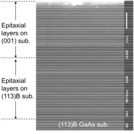
Figure 3 shows a cross-sectional image of the wafer-bonded coupled multilayer cavity observed by scanning electron microscopy (SEM). Smooth GaAs/AlGaAs inter-faces were formed over the entire region. In the structure shown in Fig. 3, two 2λ cavities were coupled by the 12.5-pair DBR to obtain the mode frequency difference of ∼ 2
Fig. 3 Cross-sectional view of the wafer-bonded coupled multilayer cavity observed by SEM.
THz while the 24- and 28-pair DBRs were formed at top and bottom sides, respectively. Note that the bonding inter-face located in the middle of the intermediate DBR could not be recognized clearly in SEM image, indicating that the de-signed coupled cavity structure was successfully fabricated. 3.2 Optical Characterization
Two mode emission from the coupled cavity was studied by optical excitation at room temperature. The excitation source was a multimode semiconductor laser with a nominal wavelength of 920 nm, which was operated in a cw mode. The laser beam was focused on the sample surface with a diameter of about 250 μm and the emitting light from the sample surface was detected using a spectrometer equipped with a cooled InGaAs photodiode array.
Figure 4 shows the emission spectra measured at var-ious wafer positions. In this sample, three layers of the QDs were embedded only in the topside cavity grown on the (001) substrate and the pairs of the top, middle, and bot-tom DBRs were 24, 12.5, and 28, respectively. The (001) epiwafer was prepared to have a few percent thickness vari-ation across the wafer, whereas the lateral thickness varia-tion of the (113)B epiwafer was as small as ∼0.2%. Due to the intentional thickness variation, the two mode emis-sion peaks were systematically shifted and the typical anti-crossing behavior could be observed by plotting the peak wavelengths of the two modes as a function of the measure-ment position (Fig. 5). Note that two cavities with identical optical thicknesses were coupled at the position where the minimum frequency difference was observed.
Let us consider emission intensity relation between the two modes when the two identical cavities are coupled. Ac-cording to the simulation by the conventional transfer
ma-Fig. 4 Emission spectra measured by optical excitation at various wafer positions.
Fig. 5 (a) Peak wavelengths of the two mode emission plotted as a func-tion of the measurement posifunc-tion. Estimated mode wavelengths before and after the bonding were indicated by broken and solid lines, respectively. (b) The frequency difference of the two mode emission peaks.
trix method, both modes show almost the same electric field distributions in the cavity region containing QDs. Thus, the emission intensity relation should be characterized by emis-sion properties of the bare QDs. Although the emisemis-sion spectrum of the bare QDs showed nearly the same sity at these two wavelengths, the measured emission inten-sity of the short-wavelength mode was much weaker than that of the long-wavelength mode as shown in Fig. 6 (c). This result was quite different from that previously observed when the entire structure was fabricated by MBE on the (001) substrate without using the wafer bonding[28]. In the case, emission intensity of each mode was almost iden-tical as expected. To understand the effect of the bonding interface, the simulated electric field distributions near the interface are shown in Fig. 6 (b). In the structure used in the initial attempt, the position of the bonding interface, which was located in the middle of the intermediate DBR as shown in Fig. 6 (a), corresponded to the anti-node of the short-wavelength mode, while it corresponded to the node of the long-wavelength mode. Consequently, optical loss caused by the bonding interface for the short-wavelength mode should be more significant compared with the long-wavelength mode. This might lead to the observed relation of the emission intensity between the two modes.
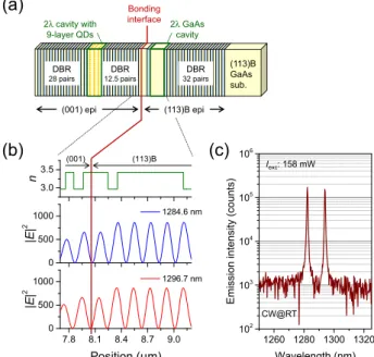
The coupled cavity structure shown in Fig. 7 (a) was designed to avoid optical loss at the bonding interface. In the intermediate DBR, aλ/4 GaAs layer nearest to the (113)B side cavity was replaced by a 3λ/4 GaAs layer. As indicated in the electric field distributions of Fig. 7 (b), one can find a position being very close to the nodes of both modes in the 3λ/4 GaAs. This position was used as the bonding interface in the next attempt. On the basis of the designed structure,
Fig. 6 (a) The structure used in the initial attempt. (b) The corresponding refractive index profile and electric field distributions of the two modes near the bonding interface. (c) The emission spectrum measured at the wafer position where the two identical cavities were coupled.
Fig. 7 (a) The structure designed to avoid optical loss at the bonding in-terface. (b) The corresponding refractive index profile and electric field distributions near the bonding interface. (c) The emission spectrum mea-sured at the wafer position where the two identical cavities were coupled.
the coupled cavity sample was fabricated in a similar man-ner as discussed above. Note that the structure contained nine QD layers in the (001) side cavity and the pairs of the top and bottom DBRs were increased to 28 and 32, respec-tively, to obtain better performance of the current-injection type devices. Figure 7 (c) shows the emission spectrum measured at the wafer position where two identical
cavi-ties were coupled. Two mode emission with identical inten-sity was clearly observed in the measured spectrum. This indicates that the optical loss at the bonding interface was greatly reduced by choosing the bonding position where the electric field had nearly zero amplitude for both modes.
4. Current-Injection Type Devices
4.1 QD Coupled Cavity
Using the coupled multilayer cavity structure shown in Fig. 7 (a), we fabricated the current-injection type devices (Fig. 8) by the following procedure. After a ring-shaped Ti/ Au (5 nm/100 nm) electrode was deposited onto the p-type DBR surface, a circular mesa with a diameter of 100 μm was formed via a following three-step wet etching process: (1) etching of the p-type DBR using a phosphoric acid solu-tion, (2) selective etching of the topside cavity using a citric acid solution, and (3) selective etching of the topmost n-AlGaAs layer of the intermediate DBR using a more diluted phosphoric acid solution. In order to realize the current con-finement structure, a thin AlAs layer inserted just above the topside cavity was selectively oxidized from the sidewall. The lateral oxidation of AlAs was accomplished by anneal-ing at 480◦C under a stem environment, which was supplied by bubbling a nitrogen gas through deionized water main-tained at 80◦C. Then, an n-type electrode was formed by depositing AuGe/Ni/Au (50 nm/12.5 nm/50 nm) onto the exposed n-type DBR surface, followed by rapid thermal an-nealing at 430◦C in nitrogen atmosphere. Finally, a poly-imide film was coated as a passivation layer. Figure 9 shows a picture of the fabricated device under room-temperature cw operation at an injection current of 10 mA. The inside di-ameter of the ring-shaped p-type electrode was 40μm, while the emission area was well restricted to a small spot with a dimeter of∼20 μm owing to the current confinement struc-ture.
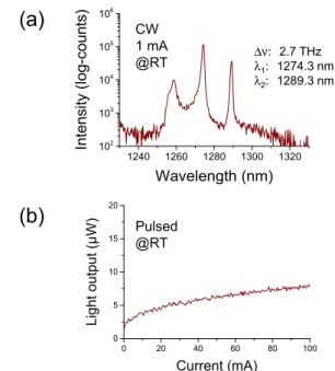
Figure 10 (a) shows the emission spectrum of the de-vice under room-temperature cw operation at 1 mA. Two
Fig. 8 A schematic of the current-injection type device.
sharp emission peaks due to the cavity modes were clearly observed at 1274.3 and 1289.3 nm. The additional small peak at 1258.4 nm was attributed to the emission from the area where the AlAs layer just above the topside cavity was selectively oxidized. The simulated optical reflection spec-trum revealed that the observed peak position corresponded to the short-wavelength mode in the region where the AlAs layer was replaced by Al2O3. Note that emission
wave-lengths of two modes from the current-injection type de-vices were almost the same as those observed in the optical excitation measurements at the corresponding wafer posi-tions. Figure 10 (b) shows the current versus light output (I-L) curve measured at room temperature using a pulsed current source with a pulse duration of 1μs and a duty cy-cle of 0.1%. Unfortunately, the measured I-L curve never showed the threshold behavior. Since the light output was almost saturated in the high current region, optical gain in the topside cavity sandwiched between the p-type and n-type DBRs seemed to be insufficient for lasing even though
Fig. 9 Top view of the fabricated device under room-temperature cw operation at 10 mA.
Fig. 10 (a) Emission spectrum of the device under room-temperature cw operation at 1 mA. (b) I-L curve measured under room-temperature pulsed operation.
Fig. 11 (a) I-L curve and (b) lasing spectrum at 40 mA of the device that contains InGaAs MQWs as optical gain media. (c) Edge emitting spectrum from the stripe-shaped mesa structure. The measurements were performed at room temperature under pulsed conditions with a pulse duration of 1μs and a duty cycle of 0.1%.
nine QD layers were introduced. An increased number of QDs by a specific stacking method would be required to en-large the optical gain enough for lasing at room temperature.
4.2 MQW Coupled Cavity
In order to realize two-color lasing from the coupled cav-ity by current injection, InGaAs multiple quantum wells (MQWs) were examined as optical gain media instead of InAs QDs. In the MQW device, an optical thickness of each cavity was set to 3λ/2 and two types of three-pair In0.15Ga0.85As/GaAs MQWs with different well widths of
3.6 and 4.4 nm were introduced only in the (001) side cav-ity. The layer structures on the (001) and (113)B wafers were designed so that two cavity modes would appear in two emission peaks of the MQWs after the bonding. Pairs of the top, middle, and bottom DBRs were 28, 12.5, and 34, respectively. The fabrication procedure was almost the same as that used for the QD devices but slightly modified. The details will be published elsewhere.
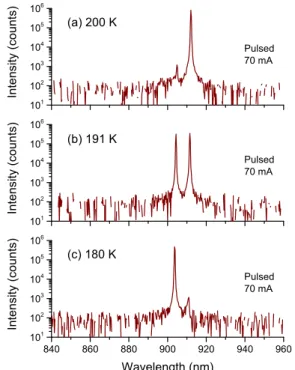
Figure 11 (a) shows the I-L curve measured under the same pulsed condition as mentioned. The threshold behav-ior was clearly observed even at room temperature. How-ever, the measured spectrum shown in Fig. 11 (b) indicated the single-color lasing due to the long-wavelength mode. In order to clarify emission peaks of the InGaAs MQWs with two different well widths, the edge-emitting spectrum shown in Fig. 11 (c) was measured for the stripe-shaped mesa structure. Comparing Figs. 11 (b) and 11 (c), we found that the wavelength mismatch between the cavity modes and gain peaks of the MQWs might cause the single-color lasing of the MQW device. The gain peaks were tuned to the cav-ity modes by lowering the operating temperature. Figure 12 shows the lasing spectra measured at 200, 191, and 180 K under a pulsed current of 70 mA. As shown in Figs. 12 (a) and 12 (c), the spectra measured at 200 and 180 K indicated
Fig. 12 Lasing spectra of the MQW device measured at (a) 200, (b) 191, and (c) 180 K under a pulse current of 70 mA.
single-color lasing due to the long- and short-wavelength modes, respectively. In contrast with this, two-color las-ing with identical intensities were successfully observed at the intermediate temperature of 191 K [Fig. 12 (b)]. The peak wavelengths were 904.4 and 911.6 nm, and the fre-quency difference was 2.6 THz. The results indicate that the intensity relation between two-color lasing in the pro-posed device can be well tuned by the operating tempera-ture. The current device is expected to emit terahertz light when the device is operated under a condition that two-color lasing is enabled. Terahertz emission would be further en-hanced by introducing nanostructured materials with excel-lent second-order nonlinearity in the (113)B side cavity. In addition, two-color laser lights should be strongly polarized in the [33¯2] direction of the (113)B epiwafer for efficient DFG. Since both the [1¯10] and [33¯2] polarization compo-nents were observed for both modes, the additional improve-ment of the device would be required for the specific polar-ization.
5. Conclusions
A semiconductor coupled multilayer cavity that consists of two cavity layers and three DBRs have been developed and studied toward novel terahertz emitting devices utiliz-ing DFG of two cavity modes. We have shown that the second-order nonlinear susceptibility have to be controlled by direct bonding of two epiwafers to achieve bright tera-hertz emission from the coupled cavity. The wafer-bonded GaAs/AlGaAs coupled multilayer cavity was fabricated us-ing the (001) and (113)B epiwafers and two-color emission due to InAs QDs only inserted in the (001) side cavity was
studied by optical excitation. We found that emission in-tensity of each mode was strongly dependent on the electric field amplitude at the bonding interface which might cause the optical loss. The optical loss could be greatly reduced by choosing the bonding position where the electric field had nearly zero amplitude for both modes. The current-injection type devices were fabricated using the wafer-bonded cou-pled multilayer cavity with nine QD layers. Unfortunately, the lasing action was never observed because of the insuffi-cient gain of the QDs. We also fabricated the MQW devices, in which two types of InGaAs MQWs were used instead of QDs. The threshold behavior was clearly observed in the
I-L curve even at room temperature. Two-color lasing was
successfully demonstrated when the gain peaks of MQWs were tuned to the cavity modes by lowering the operating temperature. This kind of device is a highly promising tera-hertz emitter because efficient DFG of the two-color laser light can be realized in the (113)B side cavity.
Acknowledgements
This work was partly supported by the Strategic Information and Communication R&D Promotion Programme (SCOPE) from the Ministry of Internal Affairs and Communications, Japan, and also by a Grant-in-Aid for Scientific Research (B) (No. 16H04351) from the Japan Society for the Promo-tion of Science (JSPS).
References
[1] M. Tonouchi, “Cutting-edge terahertz technology,” Nat. Photonics, vol.1, no.2, pp.97–105, Feb. 2007.
[2] W.L. Chan, J. Deibel, and D.M. Mittleman, “Imaging with terahertz radiation,” Rep. Prog. Phys., vol.70, no.8, pp.1325–1379, July 2007.
[3] D.H. Auston, K.P. Cheung, and P.R. Smith, “Picosecond pho-toconducting Hertzian dipoles,” Appl. Phys. Lett., vol.45, no.3, pp.284–286, Aug. 1984.
[4] P.Y. Han and X.-C. Zhang, “Coherent, broadband midinfrared tera-hertz beam sensors,” Appl. Phys. Lett., vol.73, no.21, pp.3049–3051, Nov. 1998.
[5] M. Nagai, K. Tanaka, H. Ohtake, T. Bessho, T. Sugiura, T. Hirosumi, and M. Yoshida, “Generation and detection of terahertz radiation by electro-optical process in GaAs using 1.56μm fiber laser pulses,” Appl. Phys. Lett., vol.85, no.18, pp.3974–3976, Nov. 2004.
[6] R. K¨ohler, A. Tredicucci, F. Beltram, H.E. Beere, E.H. Linfield, A.G. Davies, D.A. Ritchie, R.C. Iotti, and F. Rossi, “Terahertz semiconductor-heterostructure laser,” Nature, vol.417, no.6885, pp.156–159, May 2002.
[7] B.S. Williams, “Terahertz quantum-cascade lasers,” Nat. Photonics, vol.1, no.9, pp.517–525, Sept. 2007.
[8] M.A. Belkin, J.A. Fan, S. Hormoz, F. Capasso, S.P. Khanna, M. Lachab, A.G. Davies, and E.H. Linfield, “Terahertz quantum cas-cade lasers with copper metal-metal waveguides operating up to 178 K,” Opt. Express, vol.16, no.5, pp.3242–3248, March 2008.
[9] M. Asada, S. Suzuki, and N. Kishimoto, “Resonant tunneling diodes for sub-terahertz and terahertz oscillators,” Jpn. J. Appl. Phys., vol.47, no.6R, pp.4375–4384, June 2008.
[10] S. Suzuki, M. Asada, A. Teranishi, H. Sugiyama, and H. Yokoyama, “Fundamental oscillation of resonant tunneling diodes above 1 THz at room temperature,” Appl. Phys. Lett., vol.97, no.24, 242102, Dec. 2010.
[11] S. Matsuura, M. Tani, and K. Sakai, “Generation of coherent tera-hertz radiation by photomixing in dipole photoconductive antennas,”
Appl. Phys. Lett., vol.70, no.5, pp.559–561, Feb. 1997.
[12] H. Ito, F. Nakajima, T. Furuta, K. Yoshino, and T. Ishibashi, “Photonic terahertz-wave generation using antenna-integrated uni-travelling-carrier photodiode,” Electron. Lett., vol.39, no.25, pp.1828–1829, Dec. 2003.
[13] K. Vijayraghavan, Y. Jiang, M. Jang, A. Jiang, K. Choutagunta, A. Vizbaras, F. Demmerle, G. Boehm, M.C. Amann, and M.A. Belkin, “Broadly tunable terahertz generation in mid-infrared quantum cas-cade lasers,” Nat. Commun., vol.4, 2021, June 2013.
[14] K. Fujita, M. Hitaka, A. Ito, T. Edamura, M. Yamanishi, S. Jung, and M.A. Belkin, “Terahertz generation in mid-infrared quantum cas-cade lasers with a dual-upper-state active region,” Appl. Phys. Lett., vol.106, no.25, 251104, June 2015.
[15] N. Yamada, Y. Ichimura, S. Nakagawa, Y. Kaneko, T. Takeuchi, and N. Mikoshiba, “Second-harmonic generation in vertical-cavity surface-emitting laser,” Jpn. J. Appl. Phys., vol.35, Part 1, no.5A, pp.2659–2664, May 1996.
[16] Y. Kaneko, S. Nakagawa, Y. Ichimura, N. Yamda, D.E. Mars, and T. Takeuchi, “Blue vertical-cavity surface-emitting lasers based on second-harmonic generation grown on (311)B and (411)A GaAs substrates,” J. Appl. Phys., vol.87, no.4, pp.1597–1603, Feb. 2000.
[17] T. Kitada, F. Tanaka, T. Takahashi, K. Morita, and T. Isu, “GaAs/AlAs coupled multilayer cavity structures for terahertz emis-sion devices,” Appl. Phys. Lett., vol.95, no.11, 111106, Sept. 2009.
[18] F. Tanaka, T. Takahashi, K. Morita, T. Kitada, and T. Isu, “Strong sum frequency generation in a GaAs/AlAs coupled multilayer cavity grown on a (113)B-oriented GaAs substrate,” Jpn. J. Appl. Phys., vol.49, no.4S, 04DG01, April 2010.
[19] K. Morita, F. Tanaka, T. Takahashi, T. Kitada, and T. Isu, “Optical anisotropy of strongly enhanced sum frequency generation in (113)B GaAs/AlAs coupled multilayer cavity,” Appl. Phys. Express, vol.3, no.7, 072801, July 2010.
[20] F. Tanaka, T. Takimoto, K. Morita, T. Kitada, and T. Isu, “Time-resolved measurements of sum-frequency generation strongly en-hanced in (113)B GaAs/AlAs coupled multilayer cavity,” Jpn. J. Appl. Phys., vol.50, no.4S, 04DG03, April 2011.
[21] K. Morita, S. Katoh, T. Takimoto, F. Tanaka, Y. Nakagawa, S. Saito, T. Kitada, and T. Isu, “Generation of terahertz radiation from two cavity modes of a GaAs/AlAs coupled multilayer cavity,” Appl. Phys. Express, vol.4, no.10, 102102, Sept. 2011.
[22] S. Katoh, T. Takimoto, Y. Nakagawa, K. Morita, T. Kitada, and T. Isu, “Terahertz radiation from a (113)B GaAs/AlAs coupled multi-layer cavity generated by ultrashort laser pulse excitation,” Jpn. J. Appl. Phys., vol.51, no.4S, 04DG05, April 2012.
[23] T. Kitada, S. Katoh, T. Takimoto, Y. Nakagawa, K. Morita, and T. Isu, “Terahertz waveforms generated by second-order nonlinear po-larization in GaAs/AlAs coupled multilayer cavities using ultrashort laser pulses,” IEEE Photon. J., vol.5, no.3, 6500308, June 2013.
[24] T. Kitada, F. Tanaka, T. Takahashi, K. Morita, and T. Isu, “Novel terahertz emission devices based on efficient optical frequency con-version in GaAs/AlAs coupled multilayer cavity structures on high-index substrates,” Proc. SPIE, vol.7937, 79371H, Feb. 2011.
[25] T. Kitada, S. Katoh, T. Takimoto, Y. Nakagawa, K. Morita, and T. Isu, “Terahertz emission from a GaAs/AlAs coupled multilayer cav-ity with nonlinear optical susceptibilcav-ity inversion,” Appl. Phys. Lett., vol.102, no.25, 251118, June 2013.
[26] T. Kitada, C. Harayama, K. Morita, and T. Isu, “Two-color lasing in a coupled multilayer cavity with InAs quantum dots by optical pumping,” Phys. Status Solidi C, vol.10, no.11, pp.1434–1437, Oct. 2013.
[27] C. Harayama, S. Katoh, Y. Nakagawa, K. Morita, T. Kitada, and T. Isu, “Wafer-bonded coupled multilayer cavity with InAs quan-tum dots for two-color emission,” Jpn. J. Appl. Phys., vol.53, no.4S, 04EG11, Feb. 2014.
[28] C. Harayama, S. Katoh, Y. Nakagawa, X.M. Lu, N. Kumagai, T. Kitada, and T. Isu, “Effect of cavity-layer thicknesses on two-color emission in coupled multilayer cavities with InAs quantum dots,”
Jpn. J. Appl. Phys., vol.54, no.4S, 04DG10, March 2015.
[29] H. Ota, X.M. Lu, N. Kumagai, T. Kitada, and T. Isu, “Fabrication of two-color surface emitting device of a coupled vertical cavity structure with InAs quantum dots formed by wafer bonding,” Jpn. J. Appl. Phys., vol.55, no.4S, 04EH09, March 2016.
[30] T.R. Chung, L. Yang, N. Hosoda, H. Takagi, and T. Suga, “Wafer di-rect bonding of compound semiconductors and silicon at room tem-perature by the surface activated bonding method,” Appl. Surf. Sci., vol.117-118, pp.808–821, June 1997.
[31] H. Takagi, K. Kikuchi, R. Maeda, T.R. Chung, and T. Suga, “Sur-face activated bonding of silicon wafers at room temperature,” Appl. Phys. Lett., vol.68, no.16, pp.2222–2224, April 1996.
[32] T. Kanbara, S. Nakano, S. Yano, K. Morita, T. Kitada, and T. Isu, “Enhanced two-photon absorption in a GaAs/AlAs multilayer cav-ity,” Jpn. J. Appl. Phys., vol.48, no.4S, 04C105, April 2009.
Takahiro Kitada received B.E., M.E., and Ph.D. degrees from Osaka University, Osaka, Japan, in 1993, 1995, and 1999, respectively. From 1996 to 2006, he was a research associate of the Graduate School of Engineering Science, Osaka University, where he was engaged in re-search on molecular beam epitaxy of semicon-ductor nanostructures. In 2006, he joined the Nichia Funded Research Laboratory, Tokushima University as a designated associate professor. He is currently a designated professor of the Graduate School of Science and Technology, Tokushima University. His research interests include nonlinear optical devices based on semiconduc-tor nanostructures. He is a member of the Japan Society of Applied Physics (JSAP), the Physical Society of Japan (JPS), and the Institute of Electrical and Electronic Engineers (IEEE).
Hiroto Ota received B.E. from Tokushima University, Tokushima, Japan, in 2015. He is currently a graduate student at the Graduate School of Advanced Technology and Science, Tokushima University. He has been engaged in research on two-color surface-emitting de-vices by a GaAs-based coupled multilayer cav-ity together with faculty members of the Nichia Funded Research Laboratory, Tokushima Uni-versity. He is a graduate student member of the Japan Society of Applied Physics (JSAP).
Xiangmeng Lu received B.E. and M.E. degrees from the University of Science and Technology Beijing, China, in 2006 and 2009, respectively, and Ph.D. degree in engineering from Hokkaido University, Japan, in 2013. Since 2013, he has been a designated assistant professor at the Nichia Funded Research Labo-ratory, Tokushima University. His research in-terests include growing semiconductor nanos-tructures for nonlinear optical devices. He is a member of the Japan Society of Applied Physics (JSAP).
Naoto Kumagai received the B.E. degree in electrical and electronic engineering from Hosei University, Tokyo, Japan in 1996, and the M.E. and Ph.D. degrees in applied physics from To-hoku University, Sendai, Japan in 1998 and 2001, respectively. During the doctoral course, he was a research fellowship for young scien-tists of Japan Society for the Promotion of Sci-ence. After graduation, he joined the Joint Re-search Center for Atom Technology (JRCAT), Tsukuba, Japan, as a project research fellow. In 2002–2004, he was with the Diamond Research Center, National Institute of Advanced Industrial Science and Technology (AIST), Tsukuba, Japan, as a postdoctoral fellow. In 2004–2014, he was with the Institute of Indus-trial Science (IIS), The University of Tokyo, Tokyo, Japan, and engaged in the study on epitaxial growth of InAs quantum dots (QDs) by molecu-lar beam epitaxy for laser and single photon source applications as a des-ignated researcher and research associate. In 2014–2016, he joined the Nichia Funded Research Laboratory, Tokushima University, Tokushima, Japan, as a designated lecturer. He was engaged in the study on InAs QDs with ultrafast carrier relaxation for photoconductive switching application. In 2016, he has rejoined the AIST, Tsukuba, Japan, as a senior researcher. In the AIST, he is currently with the GaN Advanced Device Open Inno-vation Laboratory (GaN-OIL), and holds the concurrent post in the Elec-tronics and Photonics Research Institute. His research interests include the epitaxial growth of semiconductors and these optoelectronics applications. He is a member of the Japan Society of Applied Physics (JSAP).
Toshiro Isu received the B.E., M.E., and Ph.D. degrees from Osaka University in 1973, 1975, and 1978, respectively. In 1978 he joined the Central Research Laboratory, Mit-subishi Electric Corporation. In 1985–1986 he spent a year as a visiting scientist at Max-Planck Institute for Solid State Research in Stuttgart, Germany. From 1987 to 1990 he joined Opto-electronics Technology Research Laboratory in Tsukuba for the joint research project supported by Ministry of International Trade and Industry. From 2004 to 2006, he was a guest researcher in the National Institute of Information and Communication Technology (NICT) Tokyo. In 2006, he joined the University of Tokushima as a designated professor of Nichia Funded Research Laboratory, Institute of Technology and Science, and has been working on semiconductor nano-material technologies until 2016. His research interests include various aspects of semiconductor materials and optoelectronic devices such as molecular beam epitaxy, nonlinear optical responses of semiconductors, characterization of quantum structures, quan-tum dot lasers, all-optical switches, and terahertz devices. Dr. Isu is a mem-ber of The Japan Society of Applied Physics (JSAP), The Physical Society of Japan (JPS), American Physical Society (APS), The Vacuum Society of Japan, and Laser Society of Japan.