Two-color surface-emitting lasers by a GaAs-based
coupled multilayer cavity structure for coherent
terahertz light sources
Xiangmeng Lu∗, Hiroto Ota, Naoto Kumagai1, Yasuo Minami, Takahiro Kitada, Toshiro Isu
Graduate School of Science and Technology, Tokushima University, Tokushima 770-8506, Japan
Abstract
Two-color surface-emitting lasers were fabricated using a GaAs-based coupled multilayer cavity structure grown by molecular beam epitaxy. InGaAs/GaAs multiple quantum wells were introduced only in the upper cavity for two-mode emission in the near-infrared region. Two-color lasing of the device was suc-cessfully demonstrated under pulsed current operations at room temperature. We also observed good temporal coherence of the two-color laser light using a Michelson interferometer. A coherent terahertz source is expected when a wafer-bonded coupled cavity consisting of (001) and non-(001) epitaxial films is used for the two-color laser device, in which the difference-frequency generation can be enabled by the second-order nonlinear response in the lower cavity. Keywords: B3. Two-color surface-emitting laser, A3. Coupled cavity, B2. Semiconducting III-V materials, B3. Coherent terahertz source
1. Introduction
Terahertz sources have been extensively investigated because of its many potential applications, including wireless communications, spectroscopy, and
∗Corresponding author
Email address: [email protected] (Xiangmeng Lu)
1Present address: National Institute of Advanced Industrial Science and Technology (AIST), Tsukuba 305-8560, Japan
© 2017. This manuscript version is made available under the CC-BY-NC-ND 4.0 license http://creativecommons.org/licenses/by-nc-nd/4.0/ The published version is available via https://doi.org/10.1016/j.jcrysgro.2017.01.049.
imaging. Several semiconductor devices, such as quantum cascade lasers (QCLs) [1, 2, 3], resonant tunneling diodes (RTDs) [4, 5], and photomixers [6, 7] have been studied and developed for use as continuous wave (cw) terahertz emitters. Terahertz sources based on intracavity difference-frequency generation (DFG) in dual wavelength mid-infrared QCLs have also been recently reported [8, 9]. However, there are still challenges associated with each of these devices. As an example, the emission power of RTDs becomes insufficient when the devices are operated at higher frequencies. In addition, although significant progress has been made with regard to terahertz QCLs, near-room temperature operation has not been demonstrated.
Optical microcavities are good candidates for nonlinear optical devices be-cause an extremely strong electric field is realized in a cavity layer sandwiched between two distributed Bragg reflector (DBR) multilayers. In addition, effi-cient wavelength conversion is possible in a GaAs-based multilayer cavity when the structure is grown on a non-(001) substrate, taking advantage of the second-order nonlinearity of zincblende-type semiconductors [10]. In fact, blue vertical cavity surface emitting lasers (VCSELs) utilizing the second-harmonic gener-ation (SHG) on (113)B and (114)A GaAs substrates have been reported [11]. Recently, we have proposed a GaAs/AlAs coupled multilayer cavity structure for terahertz emitting devices [12]. This structure consists of two equivalent cav-ity layers and three DBR multilayers. Two cavcav-ity modes appear in the center of high reflection band as a result of coupling of the cavity layers, and the mode frequency difference can be defined in terahertz region according to the number of periods in the intermediate DBR. The electric field of each mode is greatly enhanced in both cavity layers, generating a strong frequency-mixed signal. Since the effective second-order nonlinear coefficient is zero on a (001)-oriented GaAs substrate due to crystal symmetry [10], a non-(001) substrate is essential for crystal growth. We have previously obtained a strong sum-frequency gen-eration (SFG) signal from a GaAs/AlAs coupled multilayer cavity grown on a (113)B GaAs substrate when the two modes were simultaneously excited by 100 fs laser pulses [13, 14, 15]. The peak intensity of the SFG signal was more than
400 times greater than that of the SHG from the (113)B GaAs bulk substrate. DFG signals from the (113)B coupled cavity samples were also demonstrated at room temperature by time-resolved waveform measurements using 100 fs laser pulses and a photoconductive antenna [16, 17, 18]. In addition, we found that controlling the nonlinear polarization via the face-to-face bonding of two epitax-ial wafers is an effective means of obtaining a large terahertz DFG signal from two modes [19, 20].
From the viewpoint of practical device applications, the two modes should be generated inside the structure by current injection, since this enables terahertz emission through DFG without the external light sources. Carlin et al. already demonstrated dual wavelength lasing in two-section VCSELs by current injec-tion at room temperature [21, 22]and its detailed theoretical analysis was also reported [23]. In the two-section VCSEL, both cavities had gain regions con-sisting of InGaAs multiple quantum wells (MQWs), and they also intentionally introduced an asymmetry in the two cavity length to stabilize dual wavelength laser emission. However, the use of two cavities with slightly different cavity lengths is quite unsuitable for DFG of two modes through the second-order nonlinear response inside the structure because the field overlap between two modes is largely reduced owing to the weak coupling of two cavities. Chusseau et al. studied current-injection surface-emitting devices based on strongly coupled two-cavity system that consisted of active and passive cavities [24]. However, two-color lasing was not yet experimentally demonstrated because of the struc-tural inhomogeneity. In our most recent study, current-injection two-color lasing was demonstrated using the strongly coupled two-cavity system that contains InGaAs MQWs with two different well widths only in the upper cavity layer [25]. In this paper, we report details of fabrication of the two-color lasing de-vices using GaAs/AlGaAs coupled multilayer cavity grown by molecular beam epitaxy (MBE). Temporal coherence of the two-color laser light was also studied using a Michelson interferometer to understand temporal coherence of terahertz light emitted by the DFG.
2. MBE growth and device fabrication
Our group has previously studied two mode emission resulting from optical excitation of the coupled multilayer cavity with self-assembled InAs quantum dots [26, 27], and we have recently found that significant optical loss results from the bonding interface when this interface is located at an anti-node in the electric field distribution of the mode [27]. In order to understand the intrinsic characteristics of two-color lasing in the coupled multilayer cavity, the entire structure employed in this study was prepared by solid-source MBE on a single (001) GaAs wafer.
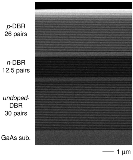
Figure 1 shows a cross-sectional scanning microscope (SEM) image of the coupled cavity structure. The structure was grown on a (001) undoped-GaAs substrate with a diameter of 2-inch using Varian GEN-II MBE system. Two types of five-period In0.2Ga0.8As/GaAs MQWs with well widths of 6.4 and 7.8 nm were introduced only in the upper 1.5 wavelength-thick (3λ/2) GaAs cavity, which was sandwiched between p- and n-type GaAs/Al0.9Ga0.1As DBRs for current injection. The periods of the top, middle and bottom DBRs were 26, 12.5, and 30, respectively. Each MQW was placed at a position where a strong electric field was present for both modes. Be and Si were used as p- and n-type dopants, respectively. The doping concentration was approximately 1.5× 1018cm−3for both the p- and n-type DBR multilayers, and a heavily Be-doped (∼1.5 × 1019 cm−3) GaAs layer was used as the p-type contact layer. A 20 nm-thick, compositionally graded digital alloy layer was inserted in each GaAs/ Al0.9Ga0.1As interface to reduce the electrical series resistance. A portion of the lower 3λ/2 GaAs cavity was grown without applying substrate rotation so that this lower cavity had a thickness distribution across the wafer. For the other layers, the substrate was rotated at 30 rpm during MBE. The nominal thickness of each layer was set to a specific value at which the cavity modes would coincide with the MQW emission peaks. The upper cavity including MQWs was grown at a substrate temperature of 500◦C, while the lower cavity and DBR multilayers were grown at 610◦C under an As4 pressure of 1× 10⁻⁵
Torr. Two Ga sources were used to set a growth rate of 1 µm/h for both GaAs and Al0.9Ga0.1As and the growth rate of InAs was 0.25 µm/h.
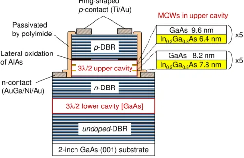
Schematic of the two-color surface-emitting device based on the coupled multilayer cavity is shown in Fig. 2. The devices were fabricated by depositing a ring-shaped Ti/Au (5 nm/100 nm) electrode onto a p-type DBR surface, after which a circular mesa with a diameter of 100 µm was formed via a three-step wet etching process. This consisted of (1) etching the p-type DBR using a phosphoric acid solution, (2) selective etching of the upper cavity using a citric acid solution, and (3) selective etching of the upper n-AlGaAs layer of the intermediate DBR using a more dilute phosphoric acid solution. In order to realize the current confinement structure, a thin AlAs layer inserted just above the upper cavity was selectively oxidized from the sidewall. This lateral oxidation of the AlAs was accomplished by annealing at 480◦C under a humid atmosphere, supplied by bubbling nitrogen gas through deionized water maintained at 80◦C. An n-type electrode was subsequently formed by depositing AuGe/Ni/Au (50 nm/12.5 nm/50 nm) onto the exposed n-type DBR surface, followed by rapid thermal annealing at 430◦C under nitrogen. Finally, a polyimide film coating was applied as a passivation layer.
3. Two-color lasing and temporal coherence
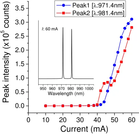
The devices were operated at room temperature using a pulsed current source with a pulse duration of 1 µs and a duty cycle of 0.1%. The light emitted from the optical window of each device was detected using a spectrometer equipped with a cooled InGaAs photodiode array. The injection current was varied from 10 to 60 mA. Two sharp emission peaks due to the cavity modes were clearly observed in all measured spectra. Figure 3 plots the intensities of the two emission peaks as a function of injection current. The inset of Fig. 3 is the spectrum measured for an injection current of 60 mA. The threshold behaviors were clearly observed for both modes with threshold currents around 40 mA. The energy separation between two laser lines was 13 meV, which corresponded
to a frequency difference of 3.1 THz. Note that two-color lasing of the device was achieved when the lower cavity had an optimal thickness relative to the upper cavity thickness and the MQW emission properties [25]. A number of devices were fabricated on a single epitaxial wafer in which the lower cavity had an intentionally induced lateral thickness variation, and the resulting emission spectra were measured at various injection-currents for each device. When the device had a relatively thin lower cavity, the long-wavelength mode exhibits threshold behavior, which was not observed for the short-wavelength mode. Conversely, a threshold was only observed for the short-wavelength mode when the device had a rather thick lower cavity. These single-color lasing behaviors can be explained by considering the electric field distribution of each mode when two cavities with different optical thicknesses are coupled. If the optical thickness of the lower cavity is less than that of the upper cavity, the electric fields of the short- and long-wavelength modes will tend to localize in the lower and upper cavities, respectively [26]. In this case, the long-wavelength mode will have a much stronger electric field in the MQW region compared to the short-wavelength mode, so that the stimulated emission will be more likely to occur in the long-wavelength mode. For similar reasons, the short-wavelength mode will be associated with stimulated emission when the lower cavity is thicker than the upper cavity. In contrast, both modes showed a threshold behavior when the lower cavity had a thickness between these two cases. Therefore, a careful adjustment of the thickness relation between the upper and lower cavities is necessary to realize two-color lasing of the proposed device.
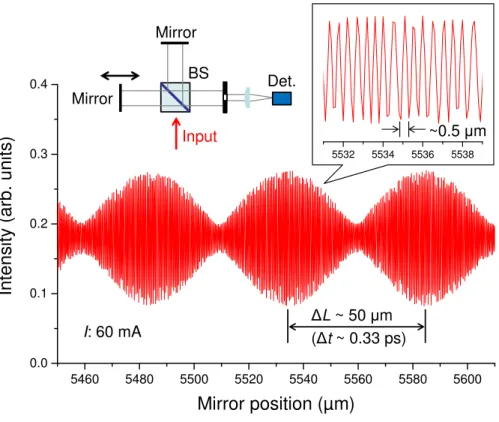
Temporal coherence of the two-color laser light was studied using a Michelson interferometer. The measured interferogram is shown in Fig.4. Two-color laser light was divided into two beams by a beam splitter and the interference signal between the light coming from two mirrors was detected using a Si photodiode. The interferogram was obtained by moving one of the mirrors using a motorized mechanical stage. The device was operated at an injection current of 60 mA under pulsed conditions with a pulse duration of 1 µs and a duty cycle of 0.1%, and a lock-in amplifier was used for the signal measurements. The intensity
oscillation with a period of∼0.5 µm can be clearly seen in the interferogram. The observed period almost corresponds to a half-wavelength of emitting laser light. Furthermore, the envelope of the oscillating signal also oscillates with a period of ∼50 µm, which is well consistent with a half-wavelength of the terahertz DFG of two-color laser light shown in Fig. 3.This oscillation behavior was clearly observed in the entire measurement range of the path difference over 1500 µm corresponding to a time delay of 10 ps. This result indicates that temporal coherence of the two-color laser light generated from the surface-emitting device based on the coupled multilayer cavity is good enough for the coherent terahertz light source by the DFG when thelowercavity is allowed to have the second-order nonlinearity.
4. Conclusions
Two-color surface-emitting lasers were successfully demonstrated using a GaAs/AlGaAs coupled multilayer cavity that consisted of two cavity layers and three DBR multilayers. Two types of five-period InGaAs/GaAs MQWs were introduced only in the upper cavity which was sandwiched between p- and n-type DBRs. Two-color lasing of the device was observed when the lower cavity had an appropriate thickness as defined by the upper cavity thickness and the MQW emission properties. Two-color laser light from the device was also characterized using a Michelson interferometer. The measured interferogram indicates that temporal coherence of the two-color laser light is good enough for the coherent terahertz light source. A coherent terahertz source is expected when thelower cavity can be responsible for DFG of two modes using a wafer-bonded coupled multilayer cavity consisting of (001) and non-(001) epitaxial films.
Acknowledgments
This work was partly supported by the Strategic Information and Com-munication R&D Promotion Programme (SCOPE) of the Ministry of Internal Affairs and Communications, Japan, and also by a Grant-in-Aid for Scientific
Research (B) (No. 16H04351) from the Japan Society for the Promotion of Science (JSPS).
References
[1] R. K¨ohler, A. Tredicucci, F. Beltram, H. E. Beere, E. H. Linfield, A. G. Davies, D. A. Ritchie, R. C. Iotti, F. Rossi, Nature 417 (2002) 156.
[2] B. S. Williams, Nat. Photonics 1 (2007) 517.
[3] M. A. Belkin, J. A. Fan, S. Hormoz, F. Capasso, S. P. Khanna, M. Lachab, A. G. Davies, E. H. Linfield, Opt. Express 16 (2008) 3242.
[4] M. Asada, S. Suzuki, N. Kishimoto, Jpn. J. Appl. Phys. 47 (2008) 4375.
[5] S. Suzuki, M. Asada, A. Teranishi, H. Sugiyama, H. Yokoyama, Appl. Phys. Lett. 97 (2010) 242102.
[6] S. Matsuura, M. Tani, K. Sakai, Appl. Phys. Lett. 70 (1997) 559.
[7] H. Ito, F. Nakajima, T. Furuta, K. Yoshino, T. Ishibashi, Electron. Lett. 39 (2003) 1828.
[8] K. Vijayraghavan, Y. Jiang, M. Jang, A. Jiang, K. Choutagunta, A. Vizbaras, F. Demmerle, G. Boehm, M. C. Amann, M. A. Belkin, Nat. Commun. 4 (2013) 2021.
[9] K. Fujita, M. Hitaka, A. Ito, T. Edamura, M. Yamanishi, S. Jung, M. A. Belkin, Appl. Phys. Lett. 106 (2015) 251104.
[10] N. Yamada, Y. Ichimura, S. Nakagawa, Y. Kaneko, T. Takeuchi, N. Mikoshiba, Jpn. J. Appl. Phys. 35 (1996) 2659.
[11] Y. Kaneko, S. Nakagawa, Y. Ichimura, N. Yamda, J. Appl. Phys. 87 (2000) 1597.
[12] T. Kitada, F. Tanaka, T. Takahashi, K. Morita, T. Isu, Appl. Phys. Lett. 95 (2009) 111106.
[13] F. Tanaka, T. Takahashi, K. Morita, T. Kitada, T. Isu, Jpn. J. Appl. Phys. 49 (2010) 04DG01.
[14] K. Morita, F. Tanaka, T. Takahashi, T. Kitada, T. Isu, Appl. Phys. Express 3 (2010) 072801.
[15] F. Tanaka, T. Takimoto, K. Morita, T. Kitada, T. Isu, Jpn. J. Appl. Phys. 50 (2011) 04DG03.
[16] K. Morita, S. Katoh, T. Takimoto, F. Tanaka, Y. Nakagawa, S. Saito, T. Kitada, T. Isu, Appl. Phys. Express 4 (2011) 102102.
[17] S. Katoh, T. Takimoto, Y. Nakagawa, K. Morita, T. Kitada, T. Isu, Jpn. J. Appl. Phys. 51 (2012) 04DG05.
[18] T. Kitada, S. Katoh, T. Takimoto, Y. Nakagawa, K. Morita, T. Isu, IEEE Photonics J. 5 (2013) 6500308.
[19] T. Kitada, F. Tanaka, T. Takahashi, K. Morita, T. Isu, Proc. SPIE 7937 (2011) 79371H.
[20] T. Kitada, S. Katoh, T. Takimoto, Y. Nakagawa, K. Morita, T. Isu, Appl. Phys. Lett. 102 (2013) 251118.
[21] J. F. Carlin, R. P. Stanley, P. Pellandini, U. Oesterle, M. Ilegems, Appl. Phys. Lett. 75 (1999) 908.
[22] M. Brunner, K. Gulden, R. H¨ovel, M. Moser, J. F. Carlin, R. P. Stanley, M. Ilegems, IEEE Photonics Technol. Lett. 12 (2000) 1316.
[23] V. Badilita, J. F. Carlin, M. Ilegems, K. Panajotov, IEEE J. Quantum Electron. 40 (2004) 1646.
[24] L. Chusseau, G. Almuneau, L. A. Coldren, A. Huntington, D. Gasquet, IEE Proc.-Optoelectron. 149 (2002) 88.
[25] T. Kitada, H. Ota, X. M. Lu, N. Kumagai, T. Isu, Appl. Phys. Express 9 (2016) 111201.
[26] C. Harayama, S. Katoh, Y. Nakagawa, X. M. Lu, N. Kumagai, T. Kitada, T. Isu, Jpn. J. Appl. Phys. 54 (2015) 04DG10.
[27] H. Ota, X. M. Lu, N. Kumagai, T. Kitada, T. Isu, Jpn. J. Appl. Phys. 55 (2016) 04EH09.
p
-DBR
26 pairs
n
-DBR
12.5 pairs
undoped
-DBR
30 pairs
GaAs sub.
1 µm
Figure 1: Cross-sectional SEM of the GaAs-based coupled multilayer cavity structure grown by MBE.
n-contact (AuGe/Ni/Au)
2-inch GaAs (001) substrate p-DBR n-DBR undoped-DBR Ring-shaped p-contact (Ti/Au) Passivated by polyimide Lateral oxidation of AlAs In x5 0.2Ga0.8As 7.8 nm GaAs 8.2 nm In0.2Ga0.8As 6.4 nm GaAs 9.6 nm x5
3λ/2 lower cavity [GaAs] 3λ/2 upper cavity
MQWs in upper cavity
Figure 2: Schematic of the two-color surface-emitting device based on the coupled multilayer cavity.
0
10
20
30
40
50
60
0.0
0.5
1.0
1.5
2.0
2.5
3.0
3.5
Peak1 [
λ
:971.4nm]
Peak2 [
λ
:981.4nm]
P
e
a
k
i
n
te
n
s
it
y
(x
1
0
5
c
o
u
n
ts
)
Current (mA)
950 960 970 980 990 1000Wavelength (nm)
Figure 3: Peak intensities of the two-color emission plotted as a function of injection current. The measurements were performed under pulsed operations at room temperature. The inset is the spectrum measured for an injection current of 60 mA.
5532 5534 5536 5538 5460 5480 5500 5520 5540 5560 5580 5600 0.0 0.1 0.2 0.3 0.4
In
te
n
s
it
y
(
a
rb
.
u
n
it
s
)
Mirror position (µm)
L~ 50 m ( t ~ 0.33 ps) BS Input Det. Mirror Mirror I: 60 mA ~0.5 mFigure 4: The interferogram of the two-color laser light measured by moving one of two mirrors in the Michelson interferometer. The device was operated by a pulsed current of 60 mA.