Japan Advanced Institute of Science and Technology Title
Fabrication of a submicron-channel organic field-effect transistor using a controllable
electrospun single fibre as a shadow mask Author(s) Ishii, Y; Sakai, H; Murata, H
Citation Nanotechnology, 22(20): 205202-205207
Issue Date 2011-03-28
Type Journal Article
Text version author
URL http://hdl.handle.net/10119/10503
Rights
Copyright (C) 2011 IOP Publishing. This is an author-created, un-copyedited version of an article accepted for publication in “Y Ishii, H Sakai, and H Murata, Nanotechnology, 22(20), 2011, 205202-205207”. IOP Publishing Ltd is not responsible for any errors or omissions in this version of the manuscript or any version derived from it. The definitive publisher-authenticated version is available online at
http://dx.doi.org/10.1088/0957-4484/22/20/205202 Description
All corresponding should be addressed to H. Murata E-mail: murata-h@jaist.ac.jp
Fabrication of a submicron-channel organic field-effect
transistor using a controllable electrospun single fibre as a
shadow mask
Y Ishii, H Sakai, and H Murata
School of Materials Science, Japan Advanced Institute of Science and Technology (JAIST), 1-1 Asahidai, Nomi, Ishikawa 923-1292, Japan
E-mail: murata-h@jaist.ac.jp
Abstract.
We demonstrate a simple and versatile method for the fabrication of a submicron channel for an organic field-effect transistor (OFET) using a single electrospun fibre as a shadow mask. A single electrospun fibre is produced by an alternative switching electrospinning method and is stretched 2.5-fold. The average diameter of the stretched fibres is 302 nm. The stretched fibre is placed on ultrathin dielectric layers of aluminium oxide and a self-assembled monolayer (SAM). The fibre acts as a very small shadow mask during electrode deposition. After removing the fibre, electrodes with very narrow gaps of around 350 nm and with high uniformity are easily obtained. We fabricate an OFET by depositing pentacene as an active layer onto the electrodes. The OFET is operable at low voltages, with a threshold voltage of -1.1 V and a sub-threshold swing of 0.27 V·decade-1, which are one order of magnitude lower than values obtained with a channel length of 75 m.
1. Introduction
In recent years, intensive study has resulted in the development of organic electronics. In particular, the organic field-effect transistor (OFET) is one promising device, as the transistor is an essential element for realizing versatile electronics [1]. Based on the scaling rule of FETs, the channel lengths in the OFET must be decreased for fast operation and increased channel current. To fabricate submicron-gap electrodes, various techniques have been developed, including photolithography, electron beam (EB) lithography [2–3], nanoimprinting [4], atomic force microscopy (AFM) lithography [5–6], and self-aligned printing [7]. Photolithography and EB
2 lithography are, for example, well-established and reliable techniques for the fabrication of submicron patterns of electrodes. However, these methods require expensive equipment and are complicated, multi-stage processes. In order to reap the benefits of low-cost organic electronics, the patterning process for the electrodes should be simple and use materials effectively.
In this paper, we demonstrate a simple and versatile technique for the fabrication of submicron-channel OFETs using a single electrospun fibre as a shadow mask. The electrospinning method has attracted much attention in the past decade as it is able to produce a large sheet composed of polymeric fibres with diameters ranging from a few micrometres to nanometres [8]. However, preparing a single, isolated fibre with the electrospinning method is quite difficult and requires advanced fabrication techniques [9–11]. Recently, we have developed a simple method for preparing a single electrospun fibre and identified an alternative switching electrospinning technique [12]. This technique allows us to control the number and diameter of submicron fibres. The alternative switching electrospinning technique also enables uniaxial alignment of the fibres. By applying the single aligned fibre as a shadow mask, we are able to fabricate submicron-gap electrodes. The performance of the fabricated OFETs is seen to be better than that of an OFET fabricated by metal shadow-masking, which produces larger channel lengths.
2. Experimental details
2.1. Materials
N-octadecylphosphonic acid was purchased from Alfa Aesar and used as received. Poly(DL-lactic acid) (PLA, Mv = 300,000–600,000) was purchased from Polyscience Inc. and used as received. Pentacene was purchased from Aldrich and purified twice by vacuum sublimation. 2-Propanol (99.9%), chloroform (99.0%), and N,N-dimethylformamide (DMF) (99.5%) were purchased from Kanto Chemical Co., Inc., and used as received.
2.2. AlOx/self-assembled monolayer gate dielectrics
To realize submicron-channel OFETs, not only the fabrication technique for the submicron-gap electrodes but also the choice of gate dielectric plays an important role. For example, the gate dielectric is required to be quite thin in order to suppress the short-channel effect. Here, we use ultrathin dielectrics (thicknesses of 6 nm or less) that are composed of an aluminium oxide (AlOx)
layer and a self-assembled monolayer (SAM) of an aliphatic phosphonic acid [13–14].
To prepare AlOx/SAM gate dielectrics, Al gate electrodes were deposited on cleaned glass
substrates with a thickness of 30 nm. Then, the Al gate electrodes were exposed to UV-O3 for 30
3 were immersed in a 2-propanol solution containing 5 mM of n-octadecylphosphonic acid. The solution was kept at room temperature and the substrates remained in solution for approximately 16 h. Substrates were then rinsed in pure 2-propanol and baked on a hotplate at 100 °C for 10 min.
2.3. Fabrication of submicron-channel OFETs
PLA was dissolved in a mixture of chloroform and DMF (chloroform:DMF = 3:2 in volume) with a concentration of 120 mg·ml-1. The solution was then loaded into a glass syringe equipped with a stainless steel needle (0.18 mm in diameter). The solution was continuously supplied using a syringe pump at a rate of 0.05 ml·h-1. The needle was connected to a high-voltage power supply (HVU-30P100, Mecc Co., Ltd.). The distance between the needle and collectors, composed of two pieces of stainless steel, was 7.5 cm and the voltage applied to the needle was 4.0 kV. Full details of the fabrication of number-controlled aligned fibres are given elsewhere [11]. Momentarily, one of the two collectors had a negative voltage (-800 V) applied while the other collector was grounded. The negatively biased electrode was switched alternatively by a switching electrode unit. Depending on switching times, number-controlled, aligned fibres were formed bridging the two collectors. Then, a certain number of the fibres were mechanically stretched in order to control the
Figure 1. Schematic illustration of fabrication of a submicron-channel OFET. STEP 1: a single
fibre is placed on the SAM/AlOx dielectrics formed on the Al gate electrodes and glass
substrates. STEP 2: the MoOx adhesion layer and Au electrode are deposited. STEP 3: the fibre
is removed manually and the submicron-gap electrodes are formed. STEP 4: pentacene is deposited onto the gap electrodes to complete the submicron-channel OFET.
4 diameter of the fibres. Here, we used a single PLA fibre which was stretched 2.5-fold from its initial length to be used as a shadow mask. Figure 1 shows a schematic illustration of our method for the fabrication of a submicron-channel OFET. The single stretched fibre was carefully placed on the AlOx/SAM gate dielectric (STEP 1). Then, a 2-nm-thick molybdenum oxide (MoOx) adhesion layer
and a 28-nm-thick Au layer were deposited on the substrates with a metal mask which defined the channel width of 200 m (STEP 2). Removing the single fibre mask formed patterned electrodes separated by a gap with a width equal to the diameter of the fibre (STEP 3). To complete the device, a 30-nm-thick pentacene layer was deposited on the gap as the active layer of the OFET (STEP 4).
2.4. Characterization
To confirm the uniformity of the fibre diameter, we measured the average diameter and standard deviation using scanning electron microscope (SEM, S-4500, Hitachi) images of six individual fibres. The average gap length (channel length for the transistors) and standard deviation of the patterned electrodes were calculated from 100 SEM images of each set of gap electrodes.
Electrical characteristics of the OFET were measured by applying a gate voltage (VG) and a
source-drain voltage (VD) with a semiconductor characterization system (4200scs, Keithley) in dry
nitrogen. Capacitances of the gate dielectric were measured with an LCR meter (4284A, Agilent) using the following capacitor layers: glass substrate/Al gate electrode/AlOx and SAM
dielectrics/MoOx (2 nm)/Au (28 nm).
3. Results and discussion
Recently, we reported diameters among electrospun fibres with twice as wide a distribution as that of diameters in an individual fibre [16]. The distribution of diameters among fibres directly affects the reproducibility of the gap length. One way to reduce this distribution is filtering by structural colour of the fibres. Kuwayama et al. reported that mats of electrospun fibres with a narrow distribution of diameters with wavelengths in the visible region show different structural colours depending on fibre diameter owing to the interference effect [15]. In this study, unstretched PLA fibres prepared by the alternative switching electrospinning method exhibited several colours among the fibres (although not within a fibre) as shown in figure 2, although PLA is transparent in the visible region. This means that the fibres have widely distributed diameters among them. Thus, we used only green-coloured single fibres as shadow masks. It should be noted that 33 fibres (figure 2) were intentionally prepared to show the difference in the colours of the fibres. For fabrication of gap electrodes, only a single fibre bridges the two collectors. The green-coloured single fibres were stretched 2.5-fold and progressed through gradual changes of colour such as
5 green → violet → yellow → greenish yellow. Figure 3(a) shows an SEM image of the single electrospun fibre stretched 2.5-fold. A uniformly aligned single fibre was obtained. We measured fibre diameters from the SEM images of the single stretched fibres (figure 3(b)). The average diameter of the fibres was 302 nm with a standard deviation of 29 nm. This fibre exhibited a very high aspect ratio of 2.5 × 10⁵ (i.e. the average fibre diameter was 302 nm and the total fibre length was 75 mm.).
By using the single 2.5-fold stretched fibre as a shadow mask, we succeeded in fabricating submicron-gap electrodes on AlOx/SAM gate dielectrics with high uniformity (figures 4(a) and (b)).
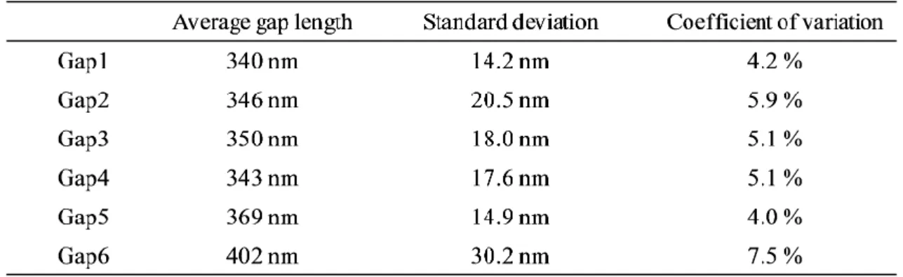
To evaluate the average gap length and standard deviation of each set of gap electrodes, we measured gap lengths at 100 points along the entire gap width of 200 m in each set of gap electrodes (figure 4(c)). To verify reproducibility and the distribution of gap lengths among multiple sets of gap electrodes, we measured six sets of gap electrodes (Gaps 1–6). Average gap lengths and standard deviations are summarized in table 1. We achieved reproducible fabrication of very narrow gap electrodes with average gap lengths ranging from 340 nm to 402 nm. The average gap lengths of the gap electrodes were slightly larger than the average diameter (302 nm) of the single fibre masks. This broadening is mainly caused by shadowing effects during the deposition process of the electrodes when we fixed the substrates during the evaporation of the layers of MoOx and Au [16].
Rotation of the substrates may further reduce the average gap lengths [17]. For precise comparison of uniformity of gap length, the coefficient of variation (ratio of standard deviation to mean value) was calculated (table 1). The coefficients of variation of the six samples ranged from 4.0% to 7.5%, which indicates very good reproducibility of fabrication.
We fabricated an OFET by depositing pentacene as an active layer onto the gap electrodes.
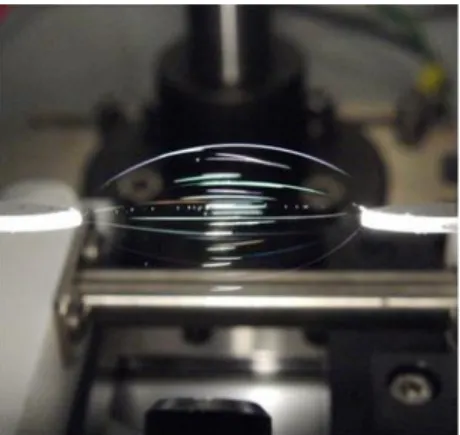
Figure 2. Photograph of unstretched PLA fibers prepared by the alternative
switching electrospinning method. Thirty-three fibers were formed bridging the two collectors.
6 Figure 5(a) shows the output characteristics of the OFET. The output characteristics are consistent with the behaviour of p-type semiconductors. Distinct saturation of drain currents (ID) and high ID
were observed at VG below -3 V. These results indicate that the short channel effect of drain currents
is effectively suppressed by the thin AlOx/SAM gate dielectrics. However, the nonlinear increase
below -1.0 V indicates the presence of contact resistance between the Au electrode and the pentacene layer. Figure 5(b) shows the transfer characteristics of the OFET at VD = -2.0 V. We
evaluated the threshold voltage (Vth) from the intercept (ID 1/2
= 0) of the plot of ID 1/2
versus VG
(figure 5(b)) of a linear fit. Carrier mobility was calculated by fitting the plot of ID 1/2
versus VG with
Figure 3. (a) SEM image of an electrospun single fibre stretched 2.5-fold. The scale bars are 5
m and 500 nm for the inset. (b) Histogram of diameters of single electrospun fibres stretched 2.5-fold. The total number of data counts is 120. The counting interval of fibre diameter is 5% of the average fibre diameter.
7
Figure 4. (a) SEM image and (b) AFM image of patterned gap electrodes. The scale bar in the
SEM image is 5 m. The inset in (a) shows a magnified SEM image of the gap electrodes (scale bar is 500 nm). (c) Histogram of gap lengths of one set of patterned electrodes (Gap 5). The total number of data counts is 100. The counting interval of the gap length is 3% of the average fibre diameter.
8
Table 1. Average gap length, standard deviation, and coefficient of variation of each set of gap
electrodes.
Figure 5. (a) Output characteristics of the OFET. (b) Transfer characteristics of the OFET at
9 the following equation [18]:
2 th G D 2L V V CW I
where is the carrier mobility, C is the capacitance per unit area of the gate dielectrics, W is the channel width (200 m), and L is the channel length (369 nm, the average gap length of the gap electrodes used). We measured C of the AlOx/SAM gate dielectrics and found the value to be 1.95
F·cm-2 at 100 Hz. This value is approximately three times the previously reported value of 0.7
F·cm-2 [13]. This would be due to insufficient formation of the SAM, which in turn was caused as a result of insufficient formation of AlOx layers and hydroxyl groups on the surface of the AlOx
layers, as we used UV-O3 treatment instead of the reported oxygen plasma treatment for the
formation of these layers. Thus, some parts of the dielectric are only composed of ultrathin, bare AlOx layers without the SAM, thus increasing the capacitance C of the dielectrics. The evaluated
values of Vth, , subthreshold swing, and on/off ratio were -1.1 V, 3.1 × 10 -3
cm2·V-1·s-1, 0.27 Vdecade-1, and 2.4 × 10³, respectively. The values of Vth and subthreshold swing are lower by one
order of magnitude than our reported values of -11.4 V and 4.1 V·decade-1, respectively, which were achieved with a channel length of 75 m [19]. However, the mobility is two orders of magnitude lower than our recently reported value of 0.16 cm2·V-1·s-1 observed with a channel length of 75 m [20]. One possibility is that there is a larger influence of contact resistance as channel length is reduced [21]. Since we prepared an OFET with a very narrow channel length compared to that of the previously reported OFET, the relative influence of contact resistance substantially increased and a quite low value was observed. Another possibility is that there was some influence of the poor quality of the gate dielectrics, which can be observed in the capacitance measurement. Inhomogeneous surfaces of gate dielectrics, such as surfaces with high roughness or with inhomogeneous surface energy, reduce mobility since the surface of gate dielectrics has a large influence on the morphology and the structural properties of active layers [22–25].
4. Conclusions
In conclusion, we demonstrated a simple and versatile technique for the fabrication of a submicron-channel OFET using a single electrospun fibre as a shadow mask. A single aligned fibre was prepared by the alternative switching electrospinning method and stretched 2.5-fold. The average diameter of the single stretched fibre was 302 nm. By employing the single fibre as a shadow mask, we succeeded in fabricating submicron-gap electrodes on ultrathin AlOx/SAM gate
dielectrics with average gap lengths of around 350 nm. Finally, we fabricated an OFET by depositing pentacene on the electrodes to act as an active layer and measured the transistor
10 characteristics of the resultant device. The threshold voltage of the OFET was -1.1 V and the subthreshold swing was 0.27 V·decade-1, which are one order of magnitude lower than values obtained for a channel length of 75 m. We believe that this method creates many opportunities for realizing high-performance, low-cost organic devices.
Acknowledgments
Y Ishii gratefully acknowledges financial support by research fellowships from the Japan Society for Promotion of Science for Young Scientists (doctoral course).
References
[1] Kymissis I 2009 Organic Field Effect Transistors (Springer, Berlin)
[2] Liu K, Avouris Ph, Bucchignano J, Martel R, Sun S and Michl J 2002 Appl. Phys. Lett. 80 865-7 [3] Tsukagoshi K, Shigeto K, Yagi I and Aoyagi Y 2006 Appl. Phys. Lett. 89 113507
[4] Chou S Y, Krauss P R and Renstrom P J 1996 Science 272 85-7 [5] Pyo S, Oh Y and Yi M 2006 Chem. Phys. Lett. 419 115-9
[6] Li L, Hirtz M, Wang W, Du C, Fuchs H and Chi L 2010 Adv. Mater. 22 1374-8 [7] Sele C W, Werne T von, Friend R H and Sirringhaus H 2005 Adv. Mater. 17 997-1001 [8] Li D and Xia Y 2004 Adv. Mater. 16 1151-70
[9] Tan E P S, Ng S Y and Lim C T 2005 Biomaterials 26 1453-6
[10] Inai R, Kotaki M and Ramakrishna S 2005 Nanotechnology 16 208-13
[11] Lee S W, Lee H J, Choi J H, Koh W G, Myoung J M, Hur J H, Park J J, Cho J H and Jeong U 2010 Nano. Lett. 10 347-51
[12] Ishii Y, Sakai H and Murata H 2008 Mater. Lett. 62 3370-2
[13] Klauk H, Zschieschang U, Pflaum J and Halik M 2007 Nature 445 745-8
[14] Jedaa A, Burkhardt M, Zschieschang U, Klauk H, Habich D, Schmid G and Halik M 2009 Org. Electron. 10 1442-7
[15] Kuwayama H, Matsumoto H, Morota K, Minagawa M and Tanioka A 2008 Sen’i Gakkaishi 64 1-4
[16] Ishii Y, Sakai H and Murata H 2009 Thin Solid Films 528 647-50
[17] Naitoh Y, Liang T-T, Azehara H and Mizutani W 2005 Jpn. J. Appl. Phys. 44 L472-4 [18] Sze S M 1981 Physics of Semiconductor Devices, 2nd ed. (Wiley, New York) [19] Sakai H, Takahashi Y and Murata H 2007 Appl. Phys. Lett. 91 113502 [20] Sakai H, Konno K and Murata H 2009 Appl. Phys. Lett. 94 073304
11 [21] Klauk H, Schmid G, Radlik W, Weber W, Zhou L, Sheraw C D, Nichols J A and Jackson T N 2003 Solid-State Electron. 47 297-301
[22] Steudel S, Vusser S D, Jonge S D, Janssen D, Verlaak S, Genoe J and Heremans P 2004 Appl. Phys. Lett. 85 4400-2
[23] Fritz S E, Kelley T W and Frisbie C D 2005 J. Phys. Chem. B 109 10574-7 [24] Knipp D, Street R A, Völkel A and Ho J 2003 J. Appl. Phys. 93 3455 [25] Yang S Y, Shin K and Park C E 2005 Adv. Funct. Mater. 15 1806-14