Mn4N thin films for spintronics applications
based on current-induced domain wall motion
著者(英)
Toshiki Gushi
year
2019
その他のタイトル
電流誘起磁壁移動に基づくスピントロニクス応用に
向けたMn4N薄膜の物性評価
学位授与大学
筑波大学 (University of Tsukuba)
学位授与年度
2018
報告番号
12102甲第8953号
URL
http://doi.org/10.15068/00156622
Mn
4
N thin films for spintronics applications based on
current-induced domain wall motion
Toshiki Gushi
Mn
4
N thin films for spintronics applications based on
current-induced domain wall motion
Toshiki Gushi
Doctoral Program in Nano-Science and Nano-Technology
Submitted to the Graduate School of
Pure and Applied Sciences
in Partial Fulfillment of the Requirements
for the Degree of Doctor of Philosophy in Engineering
at the
Outline
Extended Abstract ... 1
Introduction... 1
Magnetic domain structure in Mn4N thin films ... 1
Spin transfer torque measurement in Mn4N microstrips ... 3
Tailoring the magnetic properties by Ni-substitution into Mn4N ... 4
Summary ... 5
Introduction ... 7
State of the art ... 10
2.1. History of spintronics ... 10
2.2. Magnetic domain wall (DW) and dynamics ... 11
2.2.1. Energies in ferromagnets ... 11
2.2.2. Formation of magnetic domains ... 13
2.2.3. Magnetization dynamics ... 13
2.2.4. Spin-transfer torque (STT) ... 14
2.2.5. Current-induced domain wall motion ... 15
2.2.6. Spin-transfer torque in ferrimagnetic materials ... 17
2.3. Experimental reports of CIDWM ... 20
2.4. Anti-perovskite 3d-metal nitrides ... 22
2.4.1. Mn4N... 22
2.4.2. Substrates ... 24
Magnetic domain structure in Mn4N thin films ... 26
3.1. Growth and structure ... 26
3.1.1. MBE growth of Mn4N thin films ... 26
3.1.2. Crystallinity of the Mn4N film ... 28
3.2. Magnetic and electric properties ... 31
3.2.1. Fundamental magnetic properties ... 31
3.2.2. Magneto-transport properties ... 34
3.3. Magnetic domain structure ... 38
3.3.1. Magneto-optical Kerr effect (MOKE) imaging ... 38
3.3.2. Magnetic force microscopy (MFM) ... 39
3.3.3. Equilibrium domain size ... 40
3.4. The influence of substrates ... 41
3.5. Summary ... 42
Spin-transfer torque using direct current ... 43
4.1.3. Detailed steps for nanofabrication ... 44
4.2. Equivalency between current and magnetic field ... 45
4.3. Pinning of the DW on the notch ... 48
4.4. CIDWM without external field assistance ... 49
4.5. Summary ... 50
Evaluation of DW speed and spin-transfer efficiency ... 51
5.1. Device fabrication ... 51
5.2. Speed of DWs driven by current pulses ... 54
5.2.1. DW speed measurement ... 54
5.2.2. Current dependence of DW speed ... 55
5.2.3. Field driven Domain wall motion ... 57
5.3. Origin of the high DW mobility in Mn4N ... 58
5.4. Estimation of the spin-polarization ... 59
5.5. Influence of the non-adiabatic torque and of the damping parameter on CIDWM ... 60
5.6. Damping and non-adiabatic torque: the particular case for which = ... 61
5.7. Summary ... 62
Mn substitution by Ni in Mn4N thin films... 64
6.1. Growth and crystallinities ... 64
6.1.1. MBE growth of Mn4-xNixN ... 64
6.1.2. Crystalline quality of the Mn4-xNixN films ... 65
6.2. Magnetic and electric properties ... 65
6.2.1. VSM characterization ... 65
6.2.2. Magneto-transport properties ... 67
6.2.3. MOKE observation of the domain structure and sign of the MOKE signal ... 70
6.3. Temperature dependence of the magnetic and magneto-transports properties ... 71
6.3.1. Magnetization at low temperature ... 71
6.3.2. Magneto-transport properties at low temperature ... 74
6.4. Hypothesis of compensation by Ni atoms... 76
Total summary and prospects ... 78
Acknowledgement ... 80
Special thanks ... 82
Appendix ... 83
Cross-sectional TEM observation of Mn4N/STO interface ... 83
Voltage control of magnetic anisotropy ... 84
List of publications ... 86
Extended Abstract
Introduction
In the last 20 years, current-induced domain wall motion (CIDWM) has been studied theoretically and experimentally, mostly with the aim of discovering new ways to develop spintronic devices based on domain wall (DW) motion, such as the racetrack memory and the DW-motion MRAM. During one decade, the spin-transfer torque (STT), resulting from the transfer of angular momentum carried by the spin polarized current within the magnetic material, was the only physical effect known to allow current-induced domain wall motion. The discovery of spin-orbit torques (SOT) in multilayer systems brought more versatility and greater efficiency to CIDWM, and largely shifted the focus of the community towards spin orbitronics.
Simulations and experiments show that in perpendicularly magnetized ferrimagnets the critical current densities required to induce domain-wall motion by STT or by SOT is greatly reduced, because of the low value of the magnetization. Minimizing the operating currents allows obtaining a lower energy consumption. Thus, the combination of both STT/SOT and ferrimagnets is a very attracting pathway for creating spintronic devices based on DW motion or on nanomagnet switching.
Until now, most perpendicular ferrimagnetic materials used for DW motion experiments are rare-earth based, with a risk about material criticality in the context of the rising demand for these elements. Anti-perovskite-type nitrides with 3d transition metals are rare-earth free and could thus be interesting candidates for the replacement of the rare-earth based systems. Among them, Mn4N thin films have a high Néel temperature
TN of 745 K, a small spontaneous magnetization MS (100 kA/m) due to ferrimagnetic ordering between two
inequivalent sites, and a strong perpendicular magnetic anisotropy (PMA), with µ0HK values over 2.5 T. For the
last five years, Mn4N thin films with PMA have been successfully grown on MgO and SrTiO3(STO) substrates by
sputtering, molecular beam epitaxy (MBE), and pulse laser deposition. In this work, we have been interested in evaluating the magnetic and magneto-transport properties of Mn4N grown on STO by MBE, for the application to
spintronic devices based on CIDWM. Specifically, the fundamental properties of blanket layers, such as the magnetic anisotropy, the anomalous Hall effect, and the magnetic domain structures are studied in chapter 3, the magnitude and efficiency of STTs in Mn4N microstrips are detailed in chapters 4 and 5, and the modification of
the magnetic properties by substitution of Mn atoms by Ni is presented in chapter 6.
Magnetic domain structure in Mn
4N thin films
We have studied 10-nm-thick Mn4N epitaxial thin films grown on MgO(001) and STO(001) substrates
by MBE. Using structural characterizations, magneto-transport measurements, vibrating sample magnetometry (VSM) and magnetic imaging techniques, we studied the influence of the substrate on the magnetic properties.
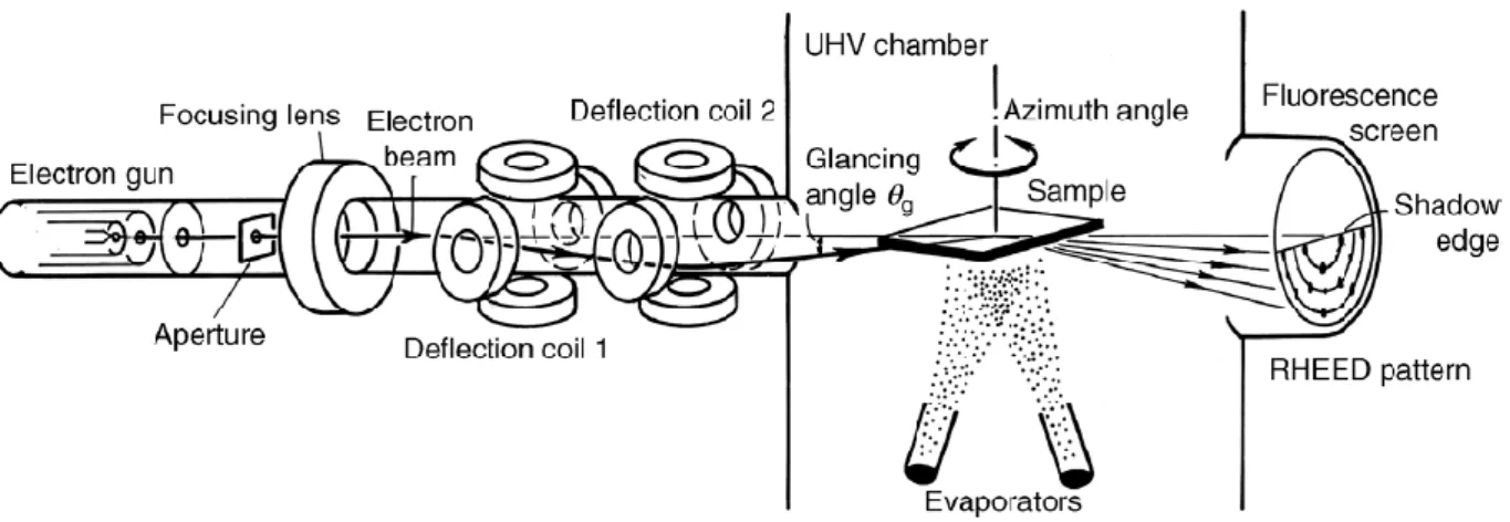
SiO2(3 nm)/Mn4N(10 nm) layers have been deposited on MgO(001) and STO(001) substrates at 450 °C,
using a MBE system. The crystalline quality of the Mn4N layer has been characterized by reflection high-energy
electron diffraction and X-ray diffraction, resulting in features common to both systems: streaky RHEED patterns, and XRD peaks of c-axis-oriented Mn4N. The full widths at half maximum (FWHM) of -scan rocking curves are
118 and 105 kA/m, respectively, in agreement with previous reports. The resistivity is 187 cm for the Mn4N/MgO sample, and 181 cm for the Mn4N/STO sample. The Anomalous Hall Effect (AHE) has been
measured by the Van der Pauw method for Mn4N blanket layers at room temperature. The AHE angle xy/xx is
high (−2%), in line with previous reports on Mn4N.
While the Mn4N/MgO sample shows a smooth hysteresis loop, the magnetization of the Mn4N/STO
sample switches very sharply, with a full remanence at zero field. Despite these differences, it is striking that the transport of the two systems are very similar, indicating that the materials are intrinsically alike. The structural characterizations suggest however that the structural disorders due to the crystalline defects are different, and thus that the increased disorder is responsible for the higher coercivity and slanted loop of Mn4N/MgO samples.
In-plane hysteresis curves obtained by in-plane AHE measurement shows that, while the magnetization of Mn4N
on MgO rises with relatively small fields, indicating a weak anisotropy, that on STO linearly increases much smoothly with the field, the anisotropy field being HK = 4.5 T. The magnetic anisotropy energy Ku, calculated
from the integration of the area enclosed between the in-plane and out-of-plane magnetization curves, and taking into account the demagnetization energy, is 0.12 MJ/m3 for MgO and 0.20 MJ/m3 for STO, respectively.
The theoretical equilibrium domain size results from the balance between the demagnetization energy and the DW energy √𝐴𝐾u, where A is an exchange stiffness. A theoretical calculation assuming a periodic stripe
domain structure concluded that the equilibrium domain size for this Mn4N film is theoretically 1.3×10¹⁰ m, much
larger than the solar system. This indicates that in this system the demagnetizing energy is negligible with respect to the DW energy, because of the small MS and high Ku, and that in practice the domain size and shape will be
rather determined by DW pinning on extrinsic defects.
After a partial reversal process, done by applying an external field close to coercive field, to reverse half of the magnetization, the magnetic domains have been observed by magnetic force microscopy (MFM) for Mn4N/MgO and by Kerr microscopy for Mn4N/STO. The sample on MgO shows sub-µm domains, much smaller
than what would be expected at equilibrium. In contrast, the sample on STO has millimeter-sized domains, a value never reported in single crystalline perpendicularly magnetized thin films (to our knowledge). MOKE images show the presence of very few nucleation centers, which means that the magnetization switching occurs by a nucleation followed by an easy propagation. This observation is consistent with the fact that the hysteresis loop is squared.
The differences between the two systems are striking, concerning both their hysteresis loops, and their domain shapes and sizes. The XRD data and the magnetic properties suggest that these differences arise from the crystalline quality of the samples, which is higher for the Mn4N/STO samples. The physical origin could arise
from the difference in the strain relaxation process: there is a large lattice misfit f = (afilm−asub)/asub at the
Mn4N/MgO interface (−7.6%), whereas the misfit at the Mn4N/STO interface is only −0.4%. While the existence
of misfit dislocations at the Mn4N/MgO interface has already been observed by transmission electron microscopy,
other strain-relaxation process through the creation of dislocations or micro-grain boundaries are also expected to play a major role in the magnetic behavior. This underlines that the selection of a well-matching substrate is crucial to improve the magnetic properties of Mn4N layers, and notably its suitability for current-induced DW
Spin transfer torque measurement in Mn
4N microstrips
The magnitude of the STT is inversely proportional to the magnetization. Thus, Mn4N thin films should
have a large STT efficiency, thanks to their small MS (~100 kA/m). However, there are only few reports about
magneto-transport properties in Mn4N, and no study of spin-transfer torques. Therefore, we aim to give light on
the potential of Mn4N thin films by evaluating the efficiency of the STT, for instance by measuring threshold
currents or DW velocities. We have used current pulses coupled to MOKE microscopy observations, and we demonstrate the potential of Mn4N as a candidate for CIDWM application by showing that standard STT can lead
to very high DW speeds in this material.
A Mn4N film grown on STO has been processed to create the 1 or 2-m-wide multi-microstrips device.
This device consists of 2 electric contacts connecting 20 strips in parallel. The current flowing through the strips can possibly induce DW motion. Under perpendicularly applied fields, the reversed domains nucleate firstly in the pad, probably because nucleation is extrinsic, and because the odds of finding a defect with a low nucleation field are bigger in a large area. Both electric contacts are covered by Ti/Au/Ti electrodes, obtained using a lift-off process. This allows wire-bonding the sample and applying the equal voltage to all the strips, and thus injecting the same current density.
The multi-strip device has been connected to the pulse generator and a 50- resistor in parallel, in order to monitor the shape of the pulse using an oscilloscope. A coil under the sample stage allows applying magnetic field pulses. The magnetic state of the device is being monitored by Kerr microscopy in differential mode. The magnitude and length of field pulses have been optimized in order to stop DWs in the middle of the strips. The direction of DW motion is opposite to the current, indicating a positive spin-polarization of the conduction electrons in Mn4N. The displacement of the DWs x is obtained by measuring the full width at half maximum of
the MOKE profile along the wire and by varying the pulse width.
The threshold current density for 1-ns-long pulse is 3.0×10¹¹ A/m2. Above 8.5×10¹¹ A/m2 in 1-m-wide
strips, the trend of the vDW-j curve becomes linear. In the studied range of current densities, the DW reached a
maximal velocity of 900 m/s, for a current density of 1.3×10¹² A/m2 in both 1-m and 2-m-wide strips. This
value is the highest in all materials and structures whose DW was driven by only pure STT, and the second highest value when looking at SOT-driven systems. Nonetheless here at room temperature.
Another figure of merit of the STT efficiency is the DW mobility 𝜂 =𝑑𝑣𝑑𝑗DW, that can be derived from the vDW-j curve, and is equal to 7.1×10⁻¹⁰ m3/C. This mobility is also the highest value in all STT-driven systems,
and it is superior to most SOT-driven records. Using the material parameters measured experimentally for the Mn4N film (MS = 71 kA/m, Ku = 0.16 MJ/m3), and assuming A = 10 pJ/m and P = 0.7, the critical current density
in our samples is expected to be jc ~ 1×10¹⁰ A/m2. This is much lower than that of a typical permalloy strip with
in-plane magnetization (jc ~ 3×10¹² A/m2), for which the non-adiabatic torque has been invoked to explain the
DW motion experimentally observed below jc.
When j >> jc, the DW moves in the precessional regime at a velocity given by, 𝒗𝐃𝐖≈1+𝛼1 2|𝒖|, where 𝒖 = 𝑔𝜇𝐵𝑃𝒋 is the spin-drift velocity, parallel to the electrons flow. Experimentally, a linear regime indeed
for the observed large DW velocities, as the mobility dvDW/dj is expected to be proportional to P/MS.
To confirm this interpretation, micromagnetic simulations have been performed. The results of the micromagnetic simulations have given an overall agreement with the 1D model and the experimental results in the high current densities regime. On the other hand, the trend of the DW speed in the low current regime is completely different from the experiment showing a relatively large critical current density of 3.0×10¹¹ A/m2. This
is due to the pinning of the DWs by defects in the actual devices while the system is supposed to be perfect without any disorder in the simulation. If the sample were perfect, we could move DW starting at Jc.
The DW velocity vDW is expected to vary linearly with the current density j, which is proportional to the
spin-drift velocity u. The spin polarization of Mn4N can be derived from the data in the high current regime,
which provide the DW mobility . Indeed, the spin polarization P is given in the 1D model by, 𝑃 = 𝜂2𝑒𝑀𝑔𝜇S
B~0.75, where e = 1.60×10⁻¹⁹ C, g = 2.0,
B = 9.27×10⁻²⁴ Am2, MS=66.1 kA/m (measured before nanofabrication) and =
7.1×10⁻¹⁰ C/m3. Note that such a high spin polarization could be of interest not only to develop CIDWM devices,
but also for magneto-resistive applications such as GMR or TMR devices.
Tailoring the magnetic properties by Ni-substitution into Mn
4N
Rare-earth based ferrimagnetic materials with PMA such as TbFeCo and GdFeCo are attracting attention because their magnetization is controllable by tuning the composition. Especially, at the angular momentum compensation point, an extremely fast DW motion driven by SOTs and magnetic fields has been reported.
In this context, Mn4N is also appealing. The ferrimagnetism of Mn4N is due to the existence of a
crystallographic sublattice for Mn, i.e. of large magnetic moment at the corner sites (I-site: I) and of small
moment at the face-centered sites (II-site: II), in contrast to rare-earth ferrimagnets where the moment of
rare-earth atoms is antiparallel to that of Fe and Co. Therefore, Mn4N can only be compensated by tuning the
composition through substitution. For the past 5 years, we have been investigating some Mn4N alloys in which
Mn was substituted by 3d metals such as Co, Fe and Ni to tune their magnetic properties. This can result in the reduction of MS in Mn4-xCoxN and Mn4-xNixN, while keeping a perpendicular magnetization. Here, we focus on
Mn4-xNixN films grown on STO, evaluating their magnetic and magneto-transport properties, and showing that it
is possible to obtain the compensation by Ni substitution.
Mn4-xNixN thin films were grown on MgO and STO substrates by molecular beam epitaxy. The nominal
content of Ni, x, has been determined from the deposition rates -measured before the growth- to be 0, 0.1, 0.25, and 0.5. Magnetization hysteresis loops have been measured by VSM, showing that Ni introduction induces a reduction of MS while conserving the perpendicular magnetization. The samples grown on STO possess a larger
MS and a more important PMA, resulting in a sharp magnetization switching. We attributed this variation of MS
and of the hysteresis loops to the difference of the crystalline qualities due to the lattice mismatch, like it has been observed for pure Mn4N films. The AHE loops of Mn4-xNixN films possess different of remanences and
magnetization reversal sharpness depending on whether they are deposited on MgO or STO.
The sign of anomalous Hall coefficients is reversed between x = 0.1 and 0.25. This sudden reversal of sign, whereas the amplitude remains high in absolute value, could be due to the crossing of the ferrimagnetic
compensation point, because the direction of the magnetic moment of 3d atoms in each sublattice changes with respect to the magnetic field. Therefore, this sign reversal is commonly used to confirm the compensation in rare-earth ferrimagnets.
We thus performed several measurements to evidence this crossing of the compensation point. The Kerr contrast has been characterized and the inversion of the Kerr contrast from x = 0.1 to x = 0.25 might also be the evidence of compensation in Mn3.75Ni0.25N.
Magnetization measurements at low temperatures have also been performed. The measurement has been performed under a magnetic field of 0.1 T. The M-T trends of x = 0 and 0.1 samples are the same, i.e., MS
increases at low temperatures, while it decreases for x = 0.25. Such a behavior has already been reported more than a half century ago, in Mn4-x(In or Sn)xN systems and attributed to the ferrimagnetic compensation.
On the assumption that the magnetic moment at the I-site (I) rises more sharply at low temperatures
than that at the II-site (II), there is a state below compensation where I dominates the total magnetization (I >
II), and MS monotonically increases as the temperature decreases. On the other hand, above the compensation
composition, II dominates the total magnetization, and the M-T curve is bended to a complex shape, with a
reduction at low temperatures. Thus, the shape of the M-T curve of Mn3.75Ni0.25N reflects the fact that the
compensation composition has been crossed.
In this thesis, we propose a model assuming a mechanism of compensation in Mn4-xNixN, where Mn
atoms at I-site are substituted by Ni atoms with smaller magnetic moment. As a result, Ni has been estimated to
be −0.7B by the fitting of composition dependence of magnetization. Such a negative value means that the
magnetic moment of Ni atoms is parallel to that of Mn atoms at II-sites, and anti-parallel to those at I-sites. The compensation composition xc has also been estimated as around x = 0.18.
Summary
The magnetic and magneto-transport properties of Mn4N thin films have been evaluated. A dramatic
improvement of these properties is obtained by replacing conventional MgO substrates by STO substrates. The Mn4N/STO system exhibits astonishing properties: a millimeter-sized domain structure, full remanence, and a
sharp magnetization switching corresponding to the nucleation of reversed domain from scarce nucleation centers and a smooth DW propagation.
The efficiency of the STT in Mn4N thin films has been evaluated by measuring the speed of DWs driven
by current pulses. The DW velocity reaches record values of 900 m/s for a current density of 1.3×10¹² A/m2,
moreover at room temperature. This value is the highest in all STT-driven systems, and is comparable to the highest speeds obtained using SOTs. The DW mobility derived from the slope of the vDW-j curve is also very
large (7.1×10⁻¹⁰ m3/C), the highest in all STT-based systems too. Fits of our data using a 1D analytical model
allows extracting a spin polarization of the conduction electrons of 0.7, suggesting that Mn4N could be suitable to
obtain large magnetoresistances.
The reduction of MS by Ni-introduction has been demonstrated, while keeping the perpendicular
temperature dependence of magnetization. The composition of the compensation point xc has been estimated to be
around 0.18. We suggest that the compensation can be understood using a simple model.
The amazing results on CIDWM have been achieved without using any rare earth element, without complex stack structures, external assistance such as magnetic/electric field, nor mechanical stress. They thus obviously reveal the potential of Mn4N thin films as a new spintronic material, consisting of only cheap elements,
Introduction
Electronics had drastically been developed since the discovery of the point-contact transistor in 1947, by Bardeen and Brattain1, and of the p-n junction bipolar transistor in 1948 by Shockley2. Semiconductor devices
solved problems posed by older devices such as vacuum tubes, such as the difficulty of the miniaturization, the high power consumption and short life time. Kilby and Noyce soon invented the integrated circuit (IC), which allows transistor miniaturization3,4. The number of transistors on one chip has increased roughly according to the
Moore’s law since then: the device density has increased exponentially, twice per 18 months to 24 months5.
Additionally, device miniaturization provided not only a higher density, but also lower power consumption, faster operation and a better yield of chips per wafer6.
This result ensured a fast development of electronics and of the associated nanofabrication technologies. Computer dimensions shrank, as well as their power consumptions, their sizes and their prices, resulting in the worldwide spread of silicon-based semiconductor technology, both for home use and for industrial applications.
However, around the end of 20th century the miniaturization process began to be slow down, because of several quantum effects or technological problems, such as the leakage of the gate charge by tunneling, which leads to an increase in power consumption, or the difficulty of nanofabrication when approaching the atomic limit, which induces a cost increase.
Severe options are envisioned to overcome these limits7:
1. More Moore: continuing miniaturization using new technologies such as extreme-ultraviolet lithography, or 3D integrations for processing and storage devices.
2. More than Moore: diversifying the functions and application of chips such as power management, interact, MEMS, sensing, etc.
3. Beyond CMOS: Employing new techniques or materials in replacement or complement of the ubiquitous silicon-based CMOS technology.
Electronics relies on control and detection of the electrons. For example, MOSFETs (Metal-oxide-Semiconductor Field Effect Transistors) enable to switch in-between two states of low and high resistance, corresponding to “0” and “1”8,9. The operation is based on the voltage control at the gate terminal of
the current through the channel. The information is stored as a charge on the gate electrodes, which acts as a capacitor. However, this information is volatile, i.e., it is lost when the power is turned off. To make matters worse, the smaller the devices, the bigger the power consumption due to the charge leakage is. Therefore, the creation of non-volatile memories, which can retain the information without power supply, is desired to reduce the static power consumption, and to obtain a normally-off computing10.
Spin electronics or Spintronics is an electronic based on the electron spin manipulation, which in its 30 years of existence has allowed developing and commercializing several applications, and which is currently
techniques such as magnetic tapes, magneto-optical disks and hard disk drives, key element of the rising age of the Big Data. In addition, the discovery of giant magnetoresistance (GMR)12,13, tunneling magnetoresistance
(TMR)14,15 and spin-transfer torque (STT)16,17 realized the fundamental spintronics concept, that is, detecting and
controlling the direction of magnetization electrically, i.e., without requirement of a magnetic field. Thus, Magnetoresistive Random Access Memories (MRAMs) a new generation of devices driven by electric currents, have been attracting attentions as embedded memories. Although MRAMs are already commercialized, they still have to compete with conventional DRAM and Flash memories, and many research projects concerning the creation of magnetic memories are in progress, from rather fundamental science to advanced technologies.
For the past two decades, current induced domain wall motion (CIDWM) devices have also been attracting attention from the spintronics communities. CIDWM is one of the phenomena caused by the STT: magnetic domain walls (DWs) move in opposite direction to the injected current, with typical speeds of 100−102
m/s. This phenomenon is expected to be used to develop memory devices such as racetrack memories18 and
DW-motion MRAM19.
After lots of efforts on soft in-plane magnetic materials such as NiFe20,21,22,23,24, the community focused
on the use of non-centrosymmetric stacks including spin-orbit materials, with Dzyaloshinskii-Moriya interaction (DMI) and perpendicular magnetization. The idea was that the spin-orbit torques (SOT), discovered in 201025,26,27
could allow obtaining small critical currents and high DW velocities.
Another way to enhance the efficiency of the current induced torque emerged more recently28,29. SOTs
are basically due to the transfer of an angular momentum, created by the Rashba-Edelstein or the spin Hall effects, to the ferromagnet magnetization. If the spontaneous magnetization is small, the ability of this angular momentum transfer to rotate the magnetization direction is expected to be high. For STT, one also aims at a perpendicular magnetization to reduce the operation current density. Therefore, rare-earth based ferrimagnetic materials with PMA such as TbFeCo or GdFeCo have been recently actively studied for CIDWM, especially close to the compensation point to minimize the spontaneous magnetization. However, the rare-earth elements have problems concerning material criticality, such as supply risk and sustainability30. Therefore, replacement of them by cheap
and abundant materials such as 3d metals is highly desirable.
In this manuscript, we will focus on a new kind of ferrimagnet thin films: anti-perovskite ferromagnetic nitrides, which are rare-earth free candidates for spintronic applications. Among them, Mn4N thin films possess
small spontaneous magnetization, around 100 kA/m, a relatively high perpendicular magnetic anisotropy, with an anisotropy field of 4 T and a perpendicular magnetization31. Such features are exciting to develop CIDWM
devices. However, there has been only few reports of the magneto-transport properties of this material, and nothing about CIDWM. The aim of my PhD was thus to explore the potential of Mn4N thin films for spintronics
application and was the aim of this joint PhD between Tsukuba and Grenoble Universities.
The manuscript is organized within 7 chapters, including this introduction. Chapter 2 provides the theoretical and experimental background concerning CIDWM and ferromagnetic nitrides. Chapter 3 gives the experimental results of measurements of the magnetic properties of Mn4N thin films, focusing on the comparison
of the growth on two different substrates, MgO and SrTiO3. Chapter 4 presents the experimental results of
CIDWM by STT under DC, measuring electrically the variation of magnetization switching fields with the applied current into microstrips devices. Chapter 5 is devoted to the measurement of DW speeds by MOKE microscopy and using current pulses. Chapter 6 introduces the magnetic properties of Mn4-xNixN alloys grown on
SrTiO3 substrates. We proposed a simple model to explain drastic variations of the magnetic properties, caused by
Ni introduction, showing that we can determine the compensation concentration of Mn4-xNixN systems. Finally, in
State of the art
2.1. History of spintronics
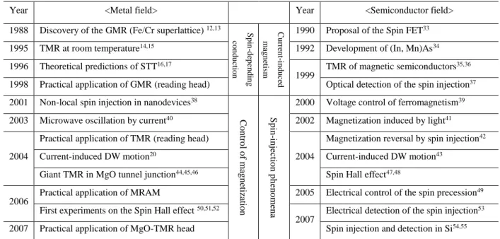
During the last 30 years, the development of spintronics, which has led to the discovery of several new phenomena, has largely benefited from the progresses in nanotechnology. Table 2-1 summarizes the chronology of spintronics research in metallic and semiconductor materials from the discovery of GMR to the middle of 2000’s, by giving a few milestones32.
In metallic systems, the discovery of magnetoresistances such as GMR and TMR were quickly used to develop read-heads for hard disk drives. The discovery, at the beginning of the century, that it is possible to control the magnetization electrically by spin-transfer torque attracted a large attention, and allowed to realize field-free operation of MRAMs. In parallel, semiconductor-based spintronics was born by doping III-V semiconductor such as InAs and GaAs by magnetic elements like Mn.
Year <Metal field> Year <Semiconductor field> 1988 Discovery of the GMR (Fe/Cr superlattice) 12,13 S
p in -d ep en d in g co n d u ct io n C u rr en t-in d u ce d mag n et ism
1990 Proposal of the Spin FET33
1995 TMR at room temperature14,15 1992 Development of (In, Mn)As34 1996 Theoretical predictions of STT16,17
1999
TMR of magnetic semiconductors35,36
1998 Practical application of GMR (reading head) Optical detection of the spin injection37 2001 Non-local spin injection in nanodevices38
Co n tr o l o f m ag n eti za ti o n S p in -in jec ti o n p h en o m en a
2000 Voltage control of ferromagnetism39
2003 Microwave oscillation by current40 2002 Magnetization induced by light41
2004
Practical application of TMR (reading head)
2004
Magnetization reversal by spin injection42
Current-induced DW motion20 Current-induced DW motion43 Giant TMR in MgO tunnel junction44,45,46 Spin Hall effect47,48
2006 Practical application of MRAM 2005 Electrical control of the spin precession 49
First experiments on the Spin Hall effect 50,51,52
2007
Electrical detection of the spin injection53
2007 Practical application of MgO-TMR head Spin injection and detection in Si54,55
Table 2-2 presents the chronology of spintronics in the last 10 years56. In the last 10 years, the interest
towards pure spin currents and spin-orbit effects increased in both metallic and semiconductor materials, replacing the focus on classical STT by spin polarized currents. Thus, the attention of the community has been directed not only towards ferromagnets and ferromagnetic semiconductor, but also towards heavy metals with strong spin-orbit interactions (such as Pt, W or Ta), topological insulators, and two-dimension electrons gas at Rashba interfaces. One of the main concepts of such a post spintronics research is spin-charge conversion: generation of pure spin current by charge current and its reverse process. Spin Hall effect (SHE) and the Rashba-Edelstein effect have realized the conversion from conventional charge current to transverse pure spin current and vice versa. In spin caloritronics, the combination of SHE and spin Seebeck effect realizes the novel thermo-electric device:
Table 2-1: Chronology of spintronics research from the discovery of GMR to the middle of 2000’s32. Important findings, research, and events related to spintronics studies are summarized by classifying them into those related to metals (left column) and to semiconductors (right column).
conversion from thermal flow to spin current (spin Seebeck effect) and from spin current to charge current (inverse SHE). Spin orbitronics includes lots of phenomena caused by spin-charge conversion57, for instance,
generation and detection of spin current, spin accumulations, producing SOT to switch magnetization and move DWs, and magnonic charge pumping.
2007 Electric field effect on metallic magnet (Electrolytic cell)58
2008
Giant spin Hall effect at RT59
Magnetization control by pure spin current60
Discovery of the Spin Seebek effect61 → Spin caloritronics 2009 Electric field effect on metallic magnet (Solid stack structure)62
2010 CoFeB/MgO MTJ with PMA 63
Discovery of spin current in ferromagnetic insulator64 2011 SOT-driven DW motion25,26,27 → Spin orbitronics 2012 The role of DMI for SOT-induced DW motion65
2013 Development of Skyrmion by DMI 66 Discovery of spin peltier effect67
2016 Mechanical production of spin current68 → Spin mechanics
2.2. Magnetic domain wall (DW) and dynamics
This work focuses on current-induced DW motion (CIDWM) in a ferrimagnetic material. Let us introduce in this section the theoretical basics of DW statics and dynamics, the torque acting on magnetic moments, and some representative reports concerning CIDWM research.
2.2.1. Energies in ferromagnets
In a magnetic system, the spatial orientation of the magnetization is determined by the balance of several magnetic energies. Let us list up the energies leading to configurations possessing magnetic domains and DWs. The contributions to the total energy are hereafter presented as energy densities. Note that in this thesis, bold letters are vectors, and the middle dot “·” corresponds to the scalar product. All formulae are in SI units.
The Zeeman energy Ez corresponds to the interaction between the magnetic field H and the
magnetization M,
𝐸z= −𝜇0𝑴 ∙ 𝑯 (2-1)
where 0 is the vacuum permeability 4×10⁻⁷ N/A2. Needless to say, the system is more stable when M and H are
parallel.
The magnetic anisotropy can be of different origins: crystalline anisotropy, shape anisotropy, or interfacial anisotropy. The shape anisotropy will be discussed later, as it actually arises from the demagnetizing field (or dipolar) energy. The magnetocrystalline anisotropy energy density Ec is determined by the relative angle
Table 2-2: Chronology of spintronics research in the last decade56, concerning metallic systems. Bold words mean the new subfields of spintronics.
given by
𝐸c= 𝐾usin2𝜃 =
𝐾u
2 (1 − cos 2𝜃) (2-2)
where Ku is the uniaxial anisotropy constant.
In this context, the interfacial anisotropy density EI, in J/m3, is given by,
𝐸I=
𝐾I
𝑡 sin2𝜃 = 𝐾I
2𝑡(1 − cos 2𝜃) (2-3)
where KI is the interfacial anisotropy constant, in J/m2, and t is the thickness of the magnetic thin films. As shown
in eq. (2-3), the volumic anisotropy density is inversely proportional to the thickness. Therefore, it is necessary to fabricate films as thin as possible to obtain large uniaxial anisotropies. For examples, Co/Pt and CoFeB/MgO systems possess relatively large interfacial anisotropies and are widely investigated for applications69,70. But
requires nanometer thick layers.
The exchange interaction between neighboring magnetic moments is a quantum effect, at the origin of ferromagnetism, ferrimagnetism, and antiferromagnetism. The energy of the exchange interaction for two neighboring spins 𝑺𝐢 and 𝑺𝐣 is given by,
𝜖ex= −𝐽𝑺𝐢∙ 𝑺𝐣 (2-4)
where J is the exchange integral. Note that this quantity is not the density per volume unit. A positive (negative) value of J leads to ferromagnetism (respectively to ferrimagnetism or antiferromagnetism). To extend this expression to continuous systems, one can note that,
𝜖ex= −𝐽𝑺𝐢∙ 𝑺𝐣 = −𝐽𝑆2cos(𝑑𝜃) ≈ −𝐽𝑆2[1 −(𝑑𝜃)2 2 ] ≈ Constant −𝐽𝑆 2𝑎2 2 (𝑑𝜃)2 𝑎2 ≈ Constant −𝐽𝑆 2𝑎2 2 ( 𝑑𝜃 𝑑𝑥) 2 (2-5) where d and a are the relative angle and the distance between neighboring moments. After normalization of the energy by the lattice volume a3 and expansion to 3D, the exchange energy density is given in a continuous model
by
𝐸ex= 𝐴(∇𝒎)2, 𝐴 =2𝑎𝐽𝑆 (2-6)
where A is the exchange stiffness constant.
The magnetic dipolar energy Ed arises from the long-distance dipolar interactions between all the
magnetic moments of the system. When the magnetization is homogeneous, and when the shape of the system is an ellipsoid (note that cylinders, spheres and thin films are ellipsoids), a simple expression of Ed can be derived, in
which a dipolar field Hd acts on the magnetization through a Zeeman-like energy,
𝐸d= −
𝜇0
2 𝑴 ∙ 𝑯𝒅, 𝑯𝒅= −𝑁̿𝑴 (2-7)
where 𝑁̿ is the demagnetizing tensor, which depends on the shape of the system. Note that the role of the dividing factor 2 is to cancel double-counting the work to move the magnetic charge against Hd caused by the
𝐸d= ∫ 𝑯𝒅∙ 𝒅𝒎 𝑀 0 = − ∫ 𝑁̿𝒎 𝒅𝒎𝑀 0 = −𝜇0 2 𝑴 ∙ 𝑯𝒅 where m is the assumed elementary magnetization.
In ferromagnetic thin films, the demagnetization tensor is diagonal with only one non-zero demagnetizing factor, along z, and equal to 1. It can be shown that in thin films, the demagnetizing field energy density can be written
𝐸d= −
𝜇0
2 𝑀S2sin2𝜃 = 𝐾dsin2𝜃 (2-8)
where Kd is called the shape anisotropy or dipolar constant, is the angle between the z axis and the
magnetization, and MS the spontaneous magnetization. The perpendicularly magnetized state has a higher energy
and is a priori unstable. Therefore, in absence of anisotropy energy and of any field, the magnetization in thin film tends to lie in-plane. This interaction is thus called shape anisotropy. Note that the expression of the shape anisotropy and of the uniaxial anisotropy (eq. 2-2) are very similar. To obtain perpendicularly magnetized thin film, the uniaxial anisotropy Ku must overcome Kd, the difference between those constants being called the
effective uniaxial anisotropy Kueff. If it is positive, the magnetization is out-of-plane.
2.2.2. Formation of magnetic domains
In a real thin film, the magnetization is not homogeneous, and the dipolar energy can be reduced by forming closed loop of stray field. Several areas, called magnetic domain, possess different directions of magnetization. From the viewpoint of minimizing the dipolar energy, the smaller the domains, the more stable the system is. However, the boundary of domains, called domain walls (DWs), have a cost in magnetic anisotropy energy and exchange energy. In a system with uniaxial anisotropy, the width of the DWs is determined by the balance between Eex and Ec, resulting in a width of ∆= √𝐴/𝐾u (a prefactor sometimes appear in this formula: as
the magnetization rotates continuously). The energy increment per surface unit due to a DW is DW=√𝐴𝐾u.
Therefore, the spatial period of domains is determined by the balance among Ed, Eex, and Ec. A quantitative
analysis of the domain period is discussed in ref. [71] and mentioned in the chapter 3 of this thesis.
2.2.3. Magnetization dynamics
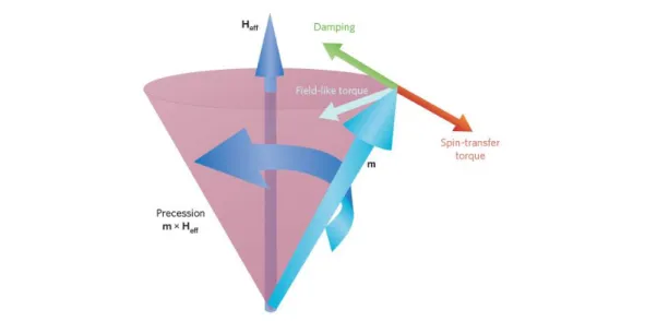
The magnetization dynamics is described in absence of spin transfer torque by the Landau- Lifshitz-Gilbert (LLG) equation72,73, given by
𝑑𝒎
𝑑𝑡 = 𝛾0𝑯𝐞𝐟𝐟× 𝒎 + 𝛼𝒎 × 𝑑𝒎
𝑑𝑡 (2-9)
where m is the unit magnetization vector (M/MS), 0 is the gyromagnetic ratio, and is the phenomenological
𝑯𝐞𝐟𝐟= −𝜇1 0𝑀S
𝑑𝐸
𝑑𝒎 (2-10)
where E is the total energy. The first term of the LLG equation corresponds to the Larmor precession of the magnetic moment around the effective field. The second term, added by Gilbert, is the damping term, which corresponds to the relaxation of the magnetic moment. Figure 2-1 shows the schematic of the torques acting on the magnetization.
2.2.4. Spin-transfer torque (STT)
In 1996, the torque caused by spin polarized current, termed spin-transfer torque (STT), has been theoretically proposed16,17. In a zone where the magnetization is rotating, such as a DW, the spin transfer can be
taken into account by adding two terms to the LLG equation74,75. For magnetic DWs,
𝑑𝒎 𝑑𝑡 = 𝛾0𝑯𝐞𝐟𝐟× 𝒎 + 𝛼𝒎 × 𝑑𝒎 𝑑𝑡 − (𝒖 ∙ 𝛁)𝒎 + 𝛽𝒎 × [(𝒖 ∙ 𝛁)𝒎] (2-11) 𝒖 =𝑔𝜇2𝑒𝑀B𝑃 S𝑱 (2-12)
where u is the spin-drift velocity, g is the g-factor, B is the Bohr magneton, P is the spin polarization of the
current, e is the elementary charge, and J is the current density vector along the direction of electrons.
The third term is the damping-like or adiabatic torque, it tends to align m with the spins of the incoming electrons. The fourth one is the field-like or non-adiabatic torque, whose direction is the same as the first term and thus assist the precession of magnetization.
Figure 2-2 presents the geometry of these four torques76. When the conduction electrons go through the
DW and enter the next domain, their spin moments rotate by 180° to be aligned with the magnetization of surrounding localized electrons. This is associated to a transfer of angular momentum to the magnetization of localized electrons, thus acting as a torque.
The existence of the STT was experimentally confirmed a few years after its prediction by current-induced magnetization switching77,78, and spin wave excitations79. This phenomenon is the key to
manipulate magnetization without magnetic field and miniaturize spintronic devices.
2.2.5. Current-induced domain wall motion
Let us now focus on current induced domain wall motion (CIDWM) in magnetic strips, which is one of the main topics of this work. CIDWM is one of the forms of STT-driven magnetization reversal80. Let us consider
a flow of electron through the DW. Figures 2-3 are schematic illustrations of a simplified CIDWM mechanism, considering only the damping-like STT. In practical systems, magnetic moments are also submitted to the precession torque, the damping torque and the field-like STT, leading to a more complex dynamics combining DW motion and magnetization precession within the DW81.
Figure 2-2: Schematic illustrations of STT76 and of the different torques acting on a magnetic moment.
Figures 2-3: Schematic illustrations of CIDWM. Arrows denote magnetic moments. Electrons flows from left side to right side. (a) When electrons go through the DW, the spins rotate to be aligned along the localized magnetic moments. As a reaction, a STT acts on the localized moments. (b) As the STT acts on localized moments, the DW moves in the same
e
-e -e-DW
e -e -STT Rotatee
-e -e- e-DW motion
(a)
(b)
e-Let us review the DW dynamics features under applied magnetic field and spin-polarized current using the 1D model proposed by Malozemoff and Slonczewski82. Figures 2-4 present the schematic of the
perpendicularly magnetized 1D model, where we assume the distribution of magnetization along y and z axis to be uniform, i.e. 𝜕𝒎𝜕𝑦 =𝜕𝒎𝜕𝑧 = 0. To describe the DW motion in the 1D model, two collective coordinates are chosen: the DW position 𝑞, and the azimuth of the magnetization in DW, 𝜑. The DW profile is described in spherical coordinates by the following ansatz:
𝜃(𝑥, 𝑡) = 2 arctan exp (𝑥 − 𝑞(𝑡)Δ ) , 𝜙(𝑥, 𝑡) = 𝜑(𝑡) (2-13) where 𝒎 = (sin 𝜃 cos 𝜙 , sin 𝜃 sin 𝜙 , cos 𝜃). Using a Lagrangian approach83 one can find the equations of
motion under a current (applied along +x) and a magnetic field applied along the easy-axis z:
1 Δ𝑞̇ − 𝛼𝜑̇ = 𝑢 Δ+ 𝜇0𝛾𝐻K 2 sin 2𝜙 , 𝜑̇ + 𝛼 Δ𝑞̇ = 𝛽 𝑢 Δ+ 𝜇0𝛾𝐻app (2-14) Here, Δ(𝜑) = √𝐾 𝐴
u+𝐾D(𝜑) is the DW width, where 𝐴 is the exchange stiffness, Ku the uniaxial anisotropy, 𝐾D=𝜇0𝑀𝑠
2
2 (𝑁xsin
2𝜑 + 𝑁
ycos2𝜑 − 𝑁z) (Ni being the demagnetizing coefficients), and 𝐻K=𝜇2𝐾D
0𝑀s is the DW demagnetizing field [75].
When a DW is driven by a magnetic field, the DW moves in the steady regime with a constant value of 𝜑 up to a field called the Walker field (HW). Above HW, the DW moves by transforming continuously, i.e., 𝜑̇ ≠
0 (from transverse to vortex DW for in-plane systems and from Bloch to Néel DW in out-of-plane systems). This continuous transformation results in a drop of the velocity until it reaches a second linear v-H regime, with reduced mobility.
When the DW is driven by a spin polarized current, in the adiabatic limit ( = 0) the DW moves continuously only when it can start precessing and align with the incoming spin polarization. This occurs above a
Figures 2-4: 1D model in magnetic strip. (a) Distribution of the magnetization in the vicinity of the DW. The orange arrows represent local magnetic moments. (b) Top view of (a). q and φ are the position of DW and the azimuth of magnetic moment in DW.
x//J
y
z
φq
(a)
(b)
x//J
y
z
φ
q
critical current density Jc given by,
𝐽c=
𝜇0𝑒
ℏ𝑃𝛥(𝜑)𝑀s𝐻K (2-15)
The last expression shows that Jc depends on the magnetization direction. In systems with in-plane
magnetization, the transverse anisotropy constant is given by 𝐾D= |𝐾z− 𝐾y| ≈ |𝐾z| =12𝜇0𝑀s2− 𝐾u . Introducing typical values, we obtain a transverse anisotropy constant of the order of 106 J/m2. On the other hand,
in thin films with perpendicular magnetization, the transverse anisotropy constant, which is related to the energy difference between a Bloch and a Néel DW, is small. In this case 𝐾D= |𝐾x− 𝐾y|. For a thin strip of thickness 𝑡
and width 𝑤, the DW can be modeled as an ellipse and the demagnetizing factors can be approximated as 𝐾x≈ 1 2𝜇0𝑀s 2( 𝑡 𝑡+𝜋𝛥 ) , 𝐾y≈ 1 2𝜇0𝑀s 2( 𝑡
𝑡+𝑤) [ 84 ]. Therefore, considering parameters of typical perpendicular
ferrimagnetic nanostrips, we obtain a transverse anisotropy constant in the order of some 104 J/m3. This implies
that the critical current density is much lower for these systems compared to systems with in-plane magnetization [85].
In the adiabatic limit, for current densities above Jc, the DW starts precessing and moves at a velocity
given by,
𝒗𝐩𝐫𝐞𝐜𝐞𝐬𝐬𝐢𝐨𝐧=1 + 𝛼1 2√𝒖𝟐− 𝒖𝐜𝟐 (2-16)
where uc is the spin-drift velocity at the critical current density. When the critical current density is very small (as
it is the case for systems with PMA), the latter expression can be approximated: 𝒗𝐩𝐫𝐞𝐜𝐞𝐬𝐬𝐢𝐨𝐧≈1 + 𝛼1 2|𝒖| =1 + 𝛼1 2 2𝑒𝑀𝑔𝜇𝐵
𝑠𝑃𝑱 (2-17)
This expression then shows that the DW mobility, vDW/J, in the precessional regime is proportional to
the ratio between the spin polarisation and the spontaneous magnetization. In conclusion, perpendicularly magnetized material with small MS and large P are the best candidates for CIDWM devices.
2.2.6. Spin-transfer torque in ferrimagnetic materials
As mentioned in the introduction, ferrimagnetic materials have been actively investigated for CIDWM applications. In ferrimagnet, the LLG equation must be modified with consideration of multiple magnetic moments in sublattices. Several modifications of conventional (i.e. considering only precession and damping) LLG equation have already been reported in refs. [86, 87, 88]. In ferrimagnetic material possessing two antiparallel magnetic moments and in each sublattice, we can express individual LLG equations for these sublattices,
𝒎̇1= 𝛾1(𝑯1+ 𝐻0𝒎2) × 𝒎1+ 𝛼1𝒎1× 𝒎̇1 (2-18)
𝒎̇2= 𝛾2(𝑯2+ 𝐻0𝒎1) × 𝒎2+ 𝛼2𝒎2× 𝒎̇2 (2-19)
where mi, i, Hi, and i are a unit vector along magnetic moment, gyromagnetic ratio, effective field, and damping
coefficient for sublattice i, respectively. H0 denotes effective field caused by exchange interaction between each
and (2-19) to be,
𝒎̇ = 𝛾eff𝑯eff× 𝒎 + 𝛼eff𝒎 × 𝒎̇ (2-20)
where m = m1 = −m2 is the unit vector along total magnetization, eff, Heffeff are the effective parameters defined
by, 𝛾eff≡𝑀𝑀1− 𝑀2 1 𝛾1 − 𝑀2 𝛾2 = 𝑀S 𝐴tot (2-21) 𝑯𝐞𝐟𝐟≡ 𝑀1𝑯𝟏− 𝑀2𝑯𝟐 𝑀1− 𝑀2 = 𝑀1𝑯𝟏− 𝑀2𝑯𝟐 𝑀S (2-22) 𝛼eff ≡ 𝛼1𝑀𝛾1 1 + 𝛼2 𝑀2 𝛾2 𝑀1 𝛾1 − 𝑀2 𝛾2 =𝛼1𝐴1+ 𝛼2𝐴2 𝐴tot (2-23)
where Mi and Ai=Mi/i are a spontaneous magnetization and an angular momentum at sublattice i, and MS, Atot are
a total spontaneous magnetization and a total angular momentum, respectively. These results indicate the existence of two singularities at compensation points of angular momentum (Atot=0) and magnetization (MS=0). At
compensation point of angular momentum where A1=A2, both eff and eff diverge, resulting in instantaneous
alignment of magnetization to the local effective field87. This divergence of
eff has been experimentally
confirmed by ferromagnetic resonance measurement in all-optical pump and probe technique88. At the
compensation point of magnetization where M1=M2, eff goes to zero and Heff diverges. However, in eq. (2-20),
Heff is multiplied by eff, canceling MS term and keeping the product finite.
A. Canizo-Cabrera et al. suggested a new modification including adiabatic STT term in CPP-GMR stack in ref. [89].Figure 2-5 illustrates the schematic diagram of the assumed geometry. Positive current means that electrons flow from free layer 1 to pinned layer 2. They formulized the STT acting to magnetic moment at i sublattice in the layer 1 as,
𝜞𝒊= ±
𝛾iℏ
𝑒𝑉 𝐼e,i𝑔i±
𝑀i 𝑴𝐢× (𝒎𝐢× 𝒎𝟑) (2-24)
where V is the volume of the layer 1, Ie,i is the electric current flowing to the sublattice i, 𝑔𝑖± is the
coefficients for sublattice i depending on the spin polarization. The combination of this torque for each sublattice introduce the effective LLG equation by,
𝒎̇ = 𝛾eff𝑯eff× 𝒎 + 𝛼eff𝒎 × 𝒎̇ ± 𝑎𝐼eff
± 𝒎 × (𝒎 × 𝒎
𝟑) (2-25)
where 𝑎𝐼±eff =𝑒𝑉ℏ 𝐼e,1𝑔1 ±+𝐼
e,2𝑔2±
𝐴tot which corresponds to the spin-drift velocity. We can say that the amplitude of STT
term diverges at the compensation point of angular momentum.
However, the authors of this report89 optimized the expression for CPP-GMR stacks and thus the vector
of STT is aligned to 𝒎 × (𝒎 × 𝒎𝟑), not to (𝜵 ∙ 𝒖)𝒎. Therefore, we derive the expression of STT in
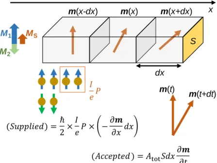
ferrimagnetic continuous wire in the context of semiclassical adiabatic description20 from the balance between
Figure 2-6 presents the schematic illustration of 1D model discussed here. We focus on the unit cell whose length is dx, cross-section is S, and unit vector of magnetization is m(x). Supplied angular momentum per unit time is calculated as the product of spin angular momentum ℏ/2, the number of flowing electrons I/e, the spin polarization of current P, and relative vector of magnetizations as given by,
(𝑆𝑢𝑝𝑝𝑙𝑖𝑒𝑑) =ℏ 2 𝐼 𝑒𝑃 × [𝒎(𝑥 − 𝑑𝑥) − 𝒎(𝑥)] = ℏ 2 𝐼 𝑒𝑃 × (− 𝜕𝒎 𝜕𝑥 𝑑𝑥) (2-26)
On the other hand, accepted angular momentum per unit time dt can be given by, (𝐴𝑐𝑐𝑒𝑝𝑡𝑒𝑑) = (𝑀1 𝛾1 − 𝑀2 𝛾2) 𝑆𝑑𝑥 𝒎(𝑡 + 𝑑𝑡) − 𝒎(𝑡) 𝑑𝑡 = 𝐴tot𝑆𝑑𝑥 𝜕𝒎 𝜕𝑡 (2-27)
STT is derived as the time derivative of magnetization vector, 𝜕𝒎 𝜕𝑡 = ℏ𝑃𝑗 2𝑒𝐴tot(− 𝜕𝒎 𝜕𝑥) = −𝑢eff 𝜕𝒎 𝜕𝑥 (2-28) 𝑢eff≡2𝑒𝐴ℏ𝑃𝑗 tot= ℏ𝛾eff𝑃𝑗 2𝑒𝑀S = 𝑔eff𝜇B𝑃𝑗 2𝑒𝑀S , (𝑔eff= ℏ𝛾eff 𝜇B ) (2-29)
Thus, the spin-drift velocity in a ferrimagnet ueff has been derived. This corresponds to replacing the g-factor in
the conventional u by an effective one. In conclusion, the spin-drift velocity in ferrimagnetic materials ueff is
diverging at the compensation point of not magnetization but angular momentum and then extremely efficient STT can be expected.
Figure 2-5: Schematic of assumed CPP-GMR stack consisting of two ferrimagnetic layers. Positive bias generates electrons flow from layer 1 to 2.89
Very recent report introduced SOT terms into ferrimagnet-LLG equations, resulting in ultrafast CIDWM at compensation temperature of angular momentum TA at 260 K28. The DW velocities in ferromagnet
(vFM) and ferrimagnet (vFiM) are obtained by replacing and by eff and eff,
𝑣FM= 𝛾 𝑀S 𝜋 2 𝐷𝑗HM √𝑗HM2 − 𝛼𝑗02 , (𝑗0= 2𝑒𝑡𝐷 ℏ𝜃SHeff∆) (2-30) 𝑣FiM=𝜋2 𝐷𝑗HM √(𝐴tot(𝑇)𝑗HM)2− (𝐴0𝑗0)2 , (𝐴0= 𝛼1𝐴1+ 𝛼2𝐴2) (2-31)
where D, jHM, t, 𝜃SHeff, and are the DMI parameter, the current density through the heavy metal layer, the
magnetic layer thickness, effective spin Hall angle, and DW width, respectively. Thus, vFiM increase with current
density linearly at the compensation point of angular momentum while vFM saturates toward D/2MS. In
conclusion, ferrimagnetic materials whose angular momentum is compensated possess singularities of , , and spin-drift velocity u and also result in high DW velocity driven by SOT.
2.3. Experimental reports of CIDWM
CIDWM has been reported since 2004. Yamaguchi et al. moved a DW in a 240-nm-wide permalloy nanostrip by current pulses20. The DW positions were detected by magnetic force microscopy. After this report,
some groups successfully achieved CIDWM in permalloy strips90,91. However, as mentioned above, the threshold
current density in in-plane magnetized strips (~1012 A/m2) is much higher than what is expected in out-of-plane
magnetized systems (~1011 A/m2). Therefore, ferromagnetic materials with PMA have soon after attracted interest
of researchers. Table 2-3 lists several examples of STT-driven CIDWM in PMA materials showing relatively high speeds, where jC is a critical current density, vmax is the maximum DW velocity, and jmax is the current density
injected to give vmax. is the DW mobility, given by the ratio vmax/jmax. If one assumes that the DW velocity in the
high current regime is proportional to the current density, corresponds to 𝑣𝐷𝑊𝑗 ~2𝑒𝑀𝑔𝜇𝐵 𝑠𝑃. Figure 2-6: Schematic illustration of supposed 1D model.
M
1M
2M
Sm(x)
m(x-dx)
m(x+dx)
dx
S
x
(𝑆𝑢𝑝𝑝𝑙𝑖𝑒𝑑) =
ℏ
2
×
𝐼
𝑒
𝑃 × −
𝜕𝒎
𝜕𝑥
𝑑𝑥
(𝐴𝑐𝑐𝑒𝑝𝑡𝑒𝑑) = 𝐴
tot𝑆𝑑𝑥
𝜕𝒎
𝜕𝑡
m(t)
m(t+dt)
𝐼
𝑒
𝑃
Among these results, ref. [92] presents quite high DW speeds for high current densities, even though the material possesses high spontaneous magnetization of 600 kA/m. The ref. [93] is also surprising, exhibiting a relatively high speed for a small current density and a high mobility. This mobility exceeds the upper limit of the spin-drift velocity with the assumption of P = 1 with MS in this system of 560 kA/m. The authors expect that
CIDWM in this system results from field-like STT and of the small Gilbert damping constant of CoB layers, accelerating the DW below the precession regime. TbFeCo possess an extremely small jC in ref. [94]. This may be
due to the fact that it is fabricated on polycarbonate substrate by nanoimprinting technique, which leads to a defect-free edge of the microstrips. However, the maximal DW speed is smaller than others by one order of magnitude.
Recently, the use of heavy metal (Pt, Ta, W, etc.) to inject pure spin currents to the ferromagnetic layers has been attracting a lot of interest. The corresponding new torque acting on magnetic moments, caused by spin Hall or Rashba-Edelstein effects, are called spin-orbit torques (SOTs). SOTs have led to faster and more efficient DW motion and magnetization switching95. Representative experimental reports with remarkable DW velocities
are listed in Table 2-4. In ref. [96], the authors employed a Pt/Co(3 Å)/Ni(7)/Co(1.5)/Ru/Co(ta)/Ni(7)/Co(tb)
multilayer structure, where the magnetization of the upper ferromagnetic layer couples anti-ferromagnetically with that of the lower layer through a RKKY interaction (synthetic antiferromagnetic structure). By tuning the thickness ta, tb and thus the total magnetization, they successfully maximized the DW speed up to 750 m/s.
In the latest report [97], the authors employed ferrimagnetic GdCo on a Pt underlayer. They changed the sample temperature and searched for the compensation points of the total magnetization and of the angular momentum, resulting in a maximum DW velocity up to 1300 m/s for 2×10¹² A/m2 at 260 K. Even at room
temperature, this system still has high DW velocity of 850 m/s, indicating the great potential of rare-earth based ferrimagnetic materials for applications to CIDWM devices.
Table 2-4: Examples of DW speeds driven by SOT in several material and systems. Material jC[1011A/m2] jmax[1011A/m2] vmax[m/s] [10-10m3/C] Ref
Pt/Co/AlOx 10 33 380 1.15 95
CoNiCo/Pt 5.0 33 750 2.27 96
GdCo/Pt(260 K) 4.4 20 1300 6.50 97
GdCo/Pt(300 K) 3.5 20 850 4.25 97
Table 2-3: The list of DW speeds driven by STT in several material and systems. Material jC[1011 A/m2] jmax[1011 A/m2] vmax[m/s] [10-10 m3/C] Ref
Co/Ni/Co 3.0 32 350 1.1 92
CoB/Ni 1.1 2.63 197 7.5 93
2.4. Anti-perovskite 3d-metal nitrides
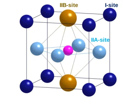
In our group in Tsukuba, we have been focusing on ferromagnetic nitrides of 3d-metals such as Fe4N98,99, Co4N100,101, Mn4N31, Ni4N102, and their alloys103,104,105, which possess an anti-perovskite structure.
Figure 2-7 exhibits the crystalline structure of such alloys, consisting of a face-centered cubic (fcc) lattice of 3d metals surrounding a body-centered nitrogen atom. Two inequivalent sites are distinguished: the corner site is the I-site whereas the face-centered sites correspond to the II-site. In consideration of hybridization effects between 2p-orbitals of N and 3d-orbitals of the metal, the II-sites can still be discomposed in between IIA and IIB sites. They possess lattice parameters of around 3.7-3.9 Å, which is close to that of Si (100) (𝑎Si/√2=3.84 Å).
Therefore, it is expected that they could be grown on commercially available Si (100)106.
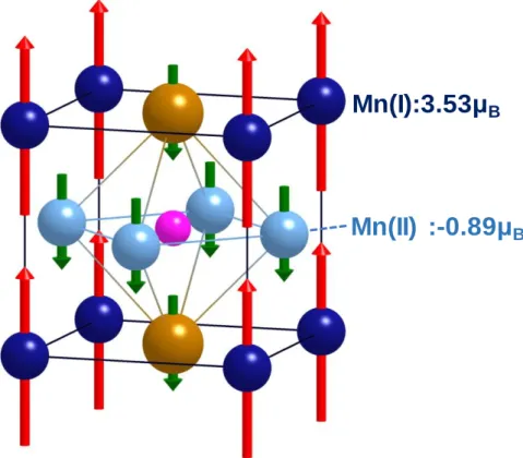
2.4.1. Mn4N
In this work, we focused on one of the 3d-metal nitrides, Mn4N. The crystalline structure with magnetic
moments is shown in Figure 2-8. Mn4N showed to be ferrimagnetic by neutron diffraction on powder samples107,
with magnetic moments of 3.53B for the I-site and -0.89 B for the II-site at 300 K. The Néel temperature TN was
also measured in the same report to be 745 K, well above room temperature. In bulk form, the magnetization easy axis is oriented in the [111] direction, with non-colinear magnetization components at II-sites108,109, tilted from the
[111] direction by 16° as illustrated in Figures 2-9110. Bulk Mn
3AN (A=Zn, Ga, etc.) alloys are actively studied
because of their large negative thermal expansion111, caused by such non-collinear magnetic structure.
While bulk Mn4N has been studied by more than half a century, thin film fabrication began more
recently in 1994112, on Si wafers, by sputtering. Table 2-5 summarizes several reports of Mn
4N thin films growth.
The first Mn4N thin films investigated already exhibited PMA, leading to a large out-of-plane remnant
magnetization Mr and coercivity HC than in-plane films, even though they possessed other phases like -Mn with
smaller MS. In ref. [113], pure Mn4N thin films, free from any secondary phase, have been deposited on
Figure 2-7: Crystalline structure of anti-perovskite nitrides.
I-site
IIA-site
6H-SiC(0001) and GaN(0001) by reactive molecular beam epitaxy (MBE). The Mn4N films were oriented along
[111] axis, showed PMA, and a high TN of 738 K, in agreement with the result obtained in bulk Mn4N107.
In the last 5 years, (001)-oriented Mn4N thin films with clearer PMA have been reported31,114,115,116,
grown on single crystalline oxide substrates such as MgO(001). These Mn4N thin film have slightly distorted
lattice of c/a~0.99, where a and c are the out-of-plane and in-plane lattice constants, of 0.389 and 0.396, respectively. Several groups have reported a relatively strong perpendicular magnetic anisotropy (Ku~1-2×10⁵
J/m3), and a small M
S of 100-200 kA/m. Magneto-transport properties have been also investigated114,116,117,118,
resulting in a relatively high and negative anomalous Hall angle AH=AH/ of -2−3% at room temperature.
However, there is still no report concerning its spin-polarization, nor STT experiment.
Figure 2-8: Crystalline structure and ferrimagnetic structure of Mn4N.
Mn(II) :-0.89μ
BTable 2-5: Reports of Mn4N growths on several substrates. † means qualitative PMA, confirmed from the out-of-plane hysteresis loops. The value of MS is measured at 300 K.
Substrate Method K
u [MJ/m 3
] c/a MS[kA/m] Orientation Reference
Si(100) Sputter
† N/A
~49 (100) and
(111) K. M. Ching et al., (1994). 119
Glass Sputter ~49 (100) K. M. Ching et al., (1995).120
SiC, GaN MBE ~80 (111) S. Dhar et al., (2005).113
MgO, STO MBE 0.22 0.99 145 (100) Y. Yasutomi et al., (2014).31
MgO PLD 0.16 0.99 157 (100) X. Shen et al., (2014).114
MgO Sputter 0.088 0.99 110 (100) K. Kabara et al., (2015).115
2.4.2. Substrates
As mentioned in the last part, most researchers working on Mn4N thin films have employed a
MgO(001) single crystalline substrate, whose structure is shown in Figures 2-10 (a). However, the lattice mismatch 𝑓 =𝑎film𝑎−𝑎sub
sub between Mn4N and MgO is large (-7.6 %), creating dislocations at the interface
114. Our
group has successfully grown Mn4N thin films on SrTiO3(STO)(001) substrates possessing a much better lattice
matching of f = -0.4 % by plasma-assisted MBE31.
In the next chapter, we will attempt to characterize the difference between deposits made on MgO and STO substrates.
Figures 2-10: Crystalline structure of (a) MgO (NaCl cell) and (b) SrTiO3 (Perovskite cell).