Japan Advanced Institute of Science and Technology
JAIST Repository
https://dspace.jaist.ac.jp/
Title
Electron transport properties of InAs ultrathin
films obtained by epitaxial lift-off and van der
Waals bonding on flexible substrates
Author(s)
Takita, Hayato; Hashimoto, Norihiko; Nguyen, Cong
Thanh; Kudo, Masahiro; Akabori, Masashi; Suzuki,
Toshi-kazu
Citation
Applied Physics Letters, 97(1): 12102-1-12102-3
Issue Date
2010-07-07
Type
Journal Article
Text version
publisher
URL
http://hdl.handle.net/10119/9495
Rights
Copyright 2010 American Institute of Physics.
This article may be downloaded for personal use
only. Any other use requires prior permission of
the author and the American Institute of Physics.
The following article appeared in Hayato Takita,
Norihiko Hashimoto, Cong Thanh Nguyen, Masahiro
Kudo, Masashi Akabori, and Toshi-kazu Suzuki,
Applied Physics Letters, 97(1), 12102- (2010) and
may be found at
http://link.aip.org/link/APPLAB/v97/i1/p012102/s1
Electron transport properties of InAs ultrathin films obtained by epitaxial
lift-off and van der Waals bonding on flexible substrates
Hayato Takita, Norihiko Hashimoto, Cong Thanh Nguyen, Masahiro Kudo, Masashi Akabori, and Toshi-kazu Suzukia兲
Center for Nano Materials and Technology, Japan Advanced Institute of Science and Technology (JAIST), 1-1 Asahidai, Nomi, Ishikawa 923-1292, Japan
共Received 13 May 2010; accepted 9 June 2010; published online 7 July 2010兲
We investigated InAs ultrathin films on flexible substrates. InAs layers grown on GaAs共001兲 are separated by epitaxial lift-off 共ELO兲, followed by van der Waals bonding 共VWB兲 on flexible substrates. We employed “normal” and “inverted” VWB; in the former, top and bottom sides are maintained during ELO and VWB, while inverted in the latter. From the InAs on flexible substrates, we fabricated Hall-bar devices with recess etch-thinning, using which electron transport properties depending on InAs layer thickness were characterized. For the inverted VWB, we observe very high electron mobilities of InAs ultrathin films, such as⬃10 000 cm2/V s for ⬃100 nm thickness and
⬃7000 cm2/V s for ⬃20 nm. These carrier mobilities are highest not only for thin films on flexible
substrates but also for InAs thin films; higher than those of InAs films grown on GaAs共111兲A and membranes fabricated from them. © 2010 American Institute of Physics.关doi:10.1063/1.3459137兴
Electron devices on flexible substrates, such as polyeth-ylene terephthalate共PET兲 substrates, are important for light-weight, portable, and flexible electronic apparatus applica-tions. In addition, flexible substrates with a low dielectric constant and a high resistivity can be advantageous for high-speed circuit applications, due to a low parasitic capacitance and a low leakage current. Thus, fabrication of high-speed and high-performance electron devices on flexible substrates is an interesting challenge for future electronics. However, in general, there are difficulties in deposition of high quality device active layers on flexible substrates due to strongly limited process temperatures and noncrystalline natures of flexible substrates. Although III-V semiconductors as a de-vice active layer have excellent electronic properties, such as high electron mobilities and velocities, deposition of high-quality III-V semiconductor thin films on flexible substrates is problematic due to the difficulties. In fact, a low-temperature-deposited polycrystalline InAs film of ⬃1 m thickness on a flexible substrate exhibits electron mobility of ⬃500 cm2/V s,1
which is far lower than that of single-crystalline InAs, while higher than that of polysingle-crystalline Si. In order to realize high-quality III-V semiconductor thin films on flexible substrates, van der Waals bonding 共VWB兲 of thin films, in combination with their separation from their original substrates, is promising because it does not involve the difficulties of the temperature limitation and the noncrys-tallinity of flexible substrates. By using the bonding method with the separation by ion-cut, a single-crystalline InP film of ⬃1 m thickness with electron mobility of⬃200 cm2/V s was formed on a flexible substrate.2On the other hand, epi-taxial lift-off共ELO兲 process3,4is simple and effective for the separation of III-V semiconductor thin films from their origi-nal substrates. While almost all studies about ELO and VWB on host substrates had been restricted to GaAs lattice-matched systems with a few exceptions,5 we recently have proposed ELO-VWB process of III-V narrow-gap
semicon-ductors obtained by lattice-mismatched growth with nano-scale thin sacrificial layers,6which can be applied for forma-tion of high-quality thin films on flexible substrates. In this work, we investigated InAs on flexible substrates obtained by the ELO-VWB process. As a result, we realized InAs ultrathin films down to ⬃20 nm thickness with very high electron mobilities on flexible substrates.
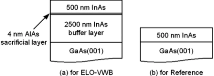
By means of molecular beam epitaxy, we grew a hetero-structure for ELO-VWB shown in Fig. 1共a兲, InAs layer 共500 nm兲/AlAs sacrificial layer 共4 nm兲/InAs buffer layer 共2500 nm兲/GaAs共001兲. For reference, a structure shown in Fig. 1共b兲, InAs layer 共500 nm兲/GaAs共001兲, was also grown. The heterostructure and the reference structure, re-spectively, exhibit room-temperature electron mobilities of 7600 cm2/V s and 7100 cm2/V s, and sheet concentrations
of 4.8⫻1012 cm−2and 3.2⫻1012 cm−2. In these structures,
there are dislocation density distributions along the growth direction.7,8 From transmission electron microscopy, we estimate dislocation density in the 500 nm InAs layer of the heterostructure, ⬃7⫻108 cm−2 near the surface and ⬃2⫻109 cm−2 at the InAs/AlAs interface. Meanwhile, the
InAs layer of the reference structure possesses estimated dislocation density ⬃2⫻109 cm−2 near the surface and
ⲏ1010 cm−2at the InAs/GaAs interface. These indicate that
the crystal quality of the InAs layer in the heterostructure is better than that in the reference structure.
Figure2shows the process of ELO and VWB on a flex-ible substrate. The flexflex-ible substrate is a PET substrate
a兲Author to whom correspondence should be addressed. Electronic mail:
[email protected]. FIG. 1.共a兲 Heterostructure for ELO-VWB. 共b兲 Reference structure.
APPLIED PHYSICS LETTERS 97, 012102共2010兲
0003-6951/2010/97共1兲/012102/3/$30.00 97, 012102-1 © 2010 American Institute of Physics
共340 m兲 coated by bisazide-rubber OMR85 共⬃500 nm兲. Using ⬃2⫻2 mm2 size samples of the heterostructure, we
carried out ELO, separation of the 500 nm InAs layer at-tached to an adhesive sheet共35 m兲, acrylic-coated polymer sheet Adwill D-201, by HF selective wet-etching of the sac-rificial layer. After the ELO, we realized two types of VWB shown in Fig. 2; one is “normal” VWB, in which top and bottom sides are maintained during ELO and VWB, and the other is “inverted” VWB, resulting in the top-bottom inver-sion. In the normal VWB process, the separated InAs layer is bonded on a flexible substrate, followed by adhesive sheet removal. On the other hand, in the inverted VWB, the sepa-rated InAs layer is first bonded on an intermediate support, a resist-coated sapphire substrate. After removal of the adhe-sive sheet, the InAs layer is transferred onto a flexible sub-strate by VWB, and then the intermediate support is removed by resist dissolution. If ELO process could be carried out after VWB of the heterostructure on a flexible substrate in the beginning, this leads to inverted VWB on the flexible substrate. However, this was impossible because a supple-ness of the adhesive sheet is necessary for progression of the selective wet-etching of the nanoscale thin sacrificial layer, whose thinness is to keep the crystal quality of the InAs layer. In order to realize firm VWB via deionized water, we employed oxide removal from the InAs surface and hydro-philic treatments using oxygen plasma of the flexible sub-strate surface. As a result, we obtained normal and inverted VWB InAs layers on flexible substrates, both of which are available for subsequent device fabrication process.
Owing to the dislocation density distribution along the growth direction in the InAs layer, the normal VWB InAs layer has lower dislocation density in the top side, while the inverted VWB InAs layer has lower dislocation density in the bottom. Therefore, we expect a different crystal quality between normal and inverted VWB after etch-thinning. This can be studied by characterization of electron transport prop-erties depending on the layer thickness using InAs Hall-bar devices with recess etch-thinning. We fabricated the Hall-bar devices from the normal VWB InAs on flexible substrate, the inverted VWB InAs on flexible substrate, and also the refer-ence InAs on GaAs共001兲, as follows. First, device mesas were isolated by wet etching. Figure 3共a兲 shows an optical microscope image of a device mesa on a flexible substrate. There was no penetration of wet etchant into the InAs/ flexible substrate interface due to the firm bonding, as con-firmed by observation from the backside of the flexible
substrate. Next, nonalloy Ohmic Ti/Au electrodes are formed by conventional metal evaporation and lift-off. Furthermore, we carried out resist patterning of the device active regions for recess etch-thinning. As shown in Fig. 3共b兲, we obtained Hall-bar devices on flexible substrates with the re-sist patterning, using which we repeated recess etch-thinning by H3PO4– H2O2– H2O wet-etchant and measurements. The
InAs layer thickness was determined by scanning confocal laser microscope measurements, with cross-checking by a step profiler. Electron transport properties were characterized by Hall measurements at room temperature.
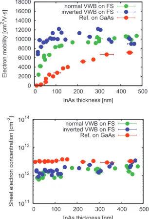
Figure4 shows electron mobilities and sheet concentra-tions as funcconcentra-tions of InAs thickness obtained by measure-ments of many devices. Both the normal and inverted VWB InAs give higher electron mobilities than that for the refer-ence, indicating that our ELO-VWB method is effective to realize high-quality InAs ultrathin films on flexible sub-strates. Moreover, in comparison with the normal VWB, the
FIG. 2.共Color兲 The process of ELO and VWB on a flexible substrate 共FS兲. Top and bottom sides are maintained in the normal VWB, while inverted in the inverted VWB.
FIG. 3. 共Color兲 Optical microscope images of 共a兲 an isolated InAs Hall-bar device mesa on a flexible substrate共FS兲 and 共b兲 a Hall-bar device on a FS with the resist patterning of the active region for recess etch-thinning.
0 2000 4000 6000 8000 10000 12000 14000 16000 18000 0 100 200 300 400 500 Electron mobility [cm 2 /V-s] InAs thickness [nm] normal VWB on FS inverted VWB on FS Ref. on GaAs 1011 1012 1013 1014 0 100 200 300 400 500 Sheet electron concentration [cm -2 ] InAs thickness [nm] normal VWB on FS inverted VWB on FS Ref. on GaAs
FIG. 4. 共Color兲 Room-temperature electron mobilities 共above兲 and sheet concentrations共below兲 for normal VWB on flexible substrate 共FS兲, inverted VWB on FS, and reference on GaAs共001兲, as functions of InAs thickness.
012102-2 Takita et al. Appl. Phys. Lett. 97, 012102共2010兲
inverted VWB InAs after thinning exhibits high electron mo-bilities as expected, such as ⬃10 000 cm2/V s for ⬃100 nm thickness and ⬃7000 cm2/V s for ⬃20 nm.
While the normal VWB and the reference give electron mo-bilities monotonically decreasing with decrease in the thick-ness, being consistent with the dislocation density distribu-tions, the inverted VWB InAs does not. For the inverted VWB InAs, with decrease in the thickness, the electron mo-bility once slightly increases for the thickness down to ⬃100 nm, which is consistent with the dislocation density distribution but followed by a decrease for the thickness ⱗ100 nm. Due to the Fermi energy pinning of InAs,9,10 there are conduction electrons accumulated at the surfaces and the interfaces共InAs/flexible substrate or InAs/GaAs兲 in spite of the undoped InAs growth. The observed sheet elec-tron concentrations are dominated by the elecelec-trons at the surfaces and the interfaces, and thus do not exhibit pro-nounced thickness dependence. The reference exhibits higher sheet electron concentrations than the normal and inverted VWB, owing to the interface electrons caused by high-density dislocations at the InAs/GaAs interface. The decrease in the electron mobilities for the inverted VWB InAs of the thickness ⱗ100 nm can be attributed to scattering of the surface electrons by the interface random potential, and also scattering of the interface electrons by the surface random potential, which should affect the electron mobilities also for the normal VWB and the reference.
For the inverted VWB InAs, we obtain highest carrier mobilities not only for thin films on flexible substrates but also for InAs thin films. Previous studies show that InAs grown on GaAs共001兲 exhibits electron mobilities similar to those of our reference, such as ⬃5000–8000 cm2/V s for
⬃500 nm thickness, ⬃2000 cm2/V s for ⬃100 nm,11,12 in-dicating difficulties of realization of high-quality InAs ultra-thin films due to the high-density dislocations at the InAs/ GaAs共001兲 interface. On the other hand, growth of InAs on GaAs共111兲A provides lower defect densities at the InAs/ GaAs interface, and thus better thin films, whose electron mobilities are ⬃3000–4000 cm2/V s for 50–100 nm thick-ness. Moreover, free-standing InAs membranes fabricated from the InAs films on GaAs共111兲A exhibit high electron mobilities such as ⬃7500 cm2/V s for 50–100 nm
thickness.13 Our inverted VWB InAs ultrathin films exhibit even higher electron mobilities. This can be applied to InAs
field effect transistors 共FETs兲,14 in particular thin-film FETs on flexible substrates, a kind of thin body III-V semiconductor-on-insulator FETs.15 In addition, we can ex-pect an extension to applications to InAs tunnel FETs.16–18
In summary, we investigated InAs ultrathin films on flexible substrates obtained by ELO-VWB. We obtained very high electron mobilities of InAs ultrathin films on flexible substrates. This can open up InAs thin-film device applica-tions on flexible substrates.
This work was partially supported by a research grant from the Foundation for Technology Promotion of Electronic Circuit Board.
1M. Takushima, Y. Kajikawa, Y. Kuya, M. Shiba, and K. Ohnishi,Jpn. J.
Appl. Phys. 47, 1469共2008兲.
2W. Chen, P. Chen, J. Pulsifer, T. Alford, T. Kuech, and S. Lau,Appl. Phys.
Lett. 92, 212109共2008兲.
3M. Konagai, M. Sugimoto, and K. Takahashi,J. Cryst. Growth 45, 277
共1978兲.
4E. Yablonovitch, T. Gmitter, J. P. Harbison, and R. Bhat,Appl. Phys. Lett.
51, 2222共1987兲.
5J. Fastenau, E. Özbay, G. Tuttle, and F. Laabs,J. Electron. Mater.24, 757
共1995兲.
6Y. Jeong, M. Shindo, M. Akabori, and T. Suzuki,Appl. Phys. Express 1,
021201共2008兲.
7J. S. Speck, M. A. Brewer, G. Beltz, A. E. Romanov, and W. Pompe,J.
Appl. Phys. 80, 3808共1996兲.
8Y. Jeong, H. Choi, and T. Suzuki,J. Cryst. Growth 301–302, 235共2007兲. 9C. A. Mead and W. G. Spitzer,Phys. Rev. Lett. 10, 471共1963兲. 10L. Ö. Olsson, C. B. M. Andersson, M. C. Håkansson, J. Kanski, L. Ilver,
and U. O. Karlsson,Phys. Rev. Lett. 76, 3626共1996兲.
11S. Kalem, J.-I. Chyi, H. Morkoç, R. Bean, and K. Zanio,Appl. Phys. Lett.
53, 1647共1988兲.
12S. P. Watkins, C. A. Tran, R. Ares, and G. Soerensen,Appl. Phys. Lett.
66, 882共1995兲.
13H. Yamaguchi, R. Dreyfus, Y. Hirayama, and S. Miyashita,Appl. Phys.
Lett. 78, 2372共2001兲.
14N. Li, E. S. Harmon, J. Hyland, D. B. Salzman, T. P. Ma, Y. Xuan, and P.
D. Ye,Appl. Phys. Lett. 92, 143507共2008兲.
15M. Yokoyama, T. Yasuda, H. Takagi, H. Yamada, N. Fukuhara, M. Hata,
M. Sugiyama, Y. Nakano, M. Takenaka, and S. Takagi,Appl. Phys. Ex-press 2, 124501共2009兲.
16Q. Zhang, W. Zhao, and A. Seabaugh,IEEE Electron Device Lett. 27, 297
共2006兲.
17S. Mookerjea and S. Datta, Proceedings of the Device Research
Confer-ence 共IEEE, New York, 2008兲, pp. 47–48, DOI: 10.1109/
DRC.2008.4800730.
18M. Luisier and G. Klimeck,IEEE Electron Device Lett. 30, 602共2009兲.
012102-3 Takita et al. Appl. Phys. Lett. 97, 012102共2010兲