A NALOGUE M IXED S IGNAL T EST D EVELOPMENT
– A C ONTINUOUS I MPROVEMENT E XERCISE I N Q UALITY , R ELIABILITY A ND R EDUCTION
I N T EST C OST O F S EMICONDUCTOR
D EVICES
Peter Sarson
Division of Electronics and Informatics Faculty of Science and Technology
Gunma University
This dissertation is submitted for the degree of Doctor of Philosophy December 2018
To my wife, Bronwen, and my children, Penelope and Amelia.
There is no elevator to success; you have to take the stairs
D ECLARATION
This dissertation is the result of my own work and includes nothing, which is the outcome of work done in collaboration except where specifically indicated in the text. It has not been previously submitted, in part or whole, to any university of institution for any degree, diploma, or other qualification.
Signed:______________________________________________________________
Date:________________________________________________________________
Peter Sarson PH.D SMIEEE CMgr MCMI Swindon, United Kingdom
Analogue Mixed Signal Test Development - Peter Sarson - December 2018
A BSTRACT
This Ph.D dissertation entitled “Analogue Mixed Signal Test Development – A Continuous Improvement Exercise in Quality, Reliability and Reduction in Test Cost of Semiconductor Devices“ by Mr. Peter Garry Sarson, BEng (Hons) CMgr MCMI SMIEEE will discuss how an automotive grade semiconductor device production test can both be improved from a test coverage and cost standpoint. Therefore ensuring both reliability and quality of the device, but also guaranteeing all specifications that normally would not be possible with lower end automated test equipment.
It will be shown experimentally how the testing of nonvolatile memories were improved such that in 5 years’ worth of high volume manufacturing, approximately 50 million devices, that not a single return was received from the field, due to a device failure, which was the result of the superior test solutions that were developed to test such devices.
It will also be shown that by exploiting the features of an automated test equipment instruments that by understanding the sampling theorem that a very efficient method can be developed for testing analog filters and similar types of circuitry such as amplifiers. Similarly by exploiting digital signal processing techniques, it will be shown how the performance of the ATE instruments can also be enhanced compared to how they are actually specified. Thus allowing difficult specification parameters that were not possible to be measured with a lower cost instrument would now become feasible to test, therefore reducing the need for more expensive test instruments and hence reducing cost of the overall test system.
A CKNOWLEDGEMENTS
First, I would sincerely like to thank Prof. Haruo Kobayashi for his encouragement to actually apply for my Ph.D. with Gunma University based on the research I have conducted as part of my career over the last 18 years. Without his guidance in all matters relating to journal and conference papers, this Ph.D. dissertation would not have been possible.
I would really like to thank my wife for her support and understanding. For several months, I spent weekends and evenings writing and re-writing my papers and my dissertation and without her support, this would not have been possible,
Thanks must also go to friends and colleagues at ams AG. Specifically Markus Wuchse, Brian Davies, Gregor Schatzberger, Fritz Leisenberger, Thomas Riener, Rainer Minixhofer, Thomas Moerth, and Herwig Klimesch for their help and support. Without their understanding that I had undertaken this endeavor, I could not have completed the required work in the shortest amount of time.
I would like to thank Prof. Haruo Kobayashi for his help and patience in getting me through this endeavor. I would also like to thank the PHD committee, Prof. Kazumasa TAKADA, Prof. Kuniyuki MOTOJIMA, Prof. Hitoshi AOKI, Prof. Koji ASAMI for reviewing my work and helping me complete this dissertation, without their help this would not have been achievable.
Last but certainly not least, I would like to show my appreciation to both Lenny Leon, Ian Harrison and Derrick Dupre at Xcerra Corporation (formally LTX) who acted somewhat like my mentors when I first came into the ATE industry. Lenny Leon originally gave me the idea for the chirp that I have developed to what it is today.
Finally, I would like to thank the discoverer of coffee, without which nothing would be possible.
C URRICULUM V ITA
1998, July23rd BEng (Hons) Electrical and Electronic Engineering with specialisation in Communications, University of Sheffield, United Kingdom.
2000, Aug 1st Senior RF Applications Engineer, LTX Corporation, United Kingdom, USA, Taiwan.
2003, Mar 1st Chartered Engineer, Institute of Electrical Engineers
2006, Dec 1st Senior Test Development Engineer, SiGe Semiconductor, United Kingdom
2007, Jan 1st Principal Test Development Engineer, Frontier Silicon, United Kingdom
2008, Nov 1st Test Development Manager, ams AG, Austria 2014, May 1st Chartered Manager, Chartered Manager Institute
2016, Mar 1st Senior Member, Institute of Electrical and Electronic Engineers 2018, Feb 1st Test Engineering Manager, Dialog Semiconductor, United
Kingdom
P UBLICATIONS
Journal Papers
[1] Peter Sarson; Haruo Kobayashi, “Using Distortion Shaping Technique to Equalize ADC THD Performance Between ATEs”, Journal of Electronic Testing: Theory and Applications, Springer (2017), DOI : 10.1007/s10836-016-5630-0
[2] Peter Sarson, G. Schatzberger, F. Leisenberger, “Fast Bit Screening of Automotive Grade EEPROMs - Continuous Improvement Exercise”, IEEE Transactions on VLSI (2017), DOI : 10.1109/TVLSI.2016.2634589
[3] Peter Sarson, “An ATE Filter Characterization ToolKit Using a Discrete Chirped Excitation Signal as Stimulus", Journal of Electronic Testing: Theory and Applications, Springer (2017), DOI : 10.1007/s10836-016-5633-x
[4] Peter Sarson; Tomonori Yanagida; Shohei Shibuya; Kosuke Machida; Haruo Kobayashi, “A Distortion Shaping Technique to Equalize Intermodulation Distortion Performance of Interpolating Arbitrary Waveform Generators in Automated Test Equipment”, Journal of Electronic Testing: Theory and Applications, Springer (2018), DOI : 10.1007/ s10836-017-5700-y
[5] Peter Sarson, “Automotive Grade Screening Procedure for Anti-Fuse Gate-Oxide Non-Volatile Memories”, IEEE Design & Test.
[6] Peter Sarson; Tomonori Yanagida; Kosuke Machida, “Measuring Group Delay of Frequency Downconverter Devices using a Chirped RF Modulated Signal”, Journal of Electronic Testing: Theory and Applications, Springer (2018), DOI : 10.1007/s10836-018-5708-y
International Conferences
[7] P. Sarson, G. Schatzberger, R. Seitz, “Automotive EEPROM Qualification and Cost Optimization”, IEEE 22nd Asian Test Symposium, pp. 105-106, Yilan, Taiwan (2013).
[8] Peter Sarson, “Analog DfT & Test : implementing analog Iddq”, 2014 19th IEEE European Test Symposium (ETS), ETS2 – Special Track on Emerging Test Solutions
[9] (Invited) Peter Sarson, “RF Filter Characterization Using a Chirp” , IEEE 9th International Design & Test Symposium, Algiers, Algeria (Dec. 2014).
[10] Peter Sarson, “ACR BER correlation to ATE for a COFDM VHF RX”, 20th International Mixed-Signal Testing Workshop, pp.1 - 4, Paris, France (2015).
[11] Peter Sarson, “Very Low Supply Voltage Room Temperature Test to Screen Low Temperature Soft Blown Fuse Fails Which Result in a Resistive Bridge“, 17th International Symposium on Quality Electronic Design, pp.135 - 139, Santa Clara, CA (May 2016).
[12] G. Schatzberger, F. P Leisenberger, P. Sarson, “Yield Improvement of an EEPROM for Automotive Applications While Maintaining High Reliability”, IEEE 34th VLSI Test Symposium, pp. 1-6, Las Vegas, NV (April 2016).
[13] Peter Sarson, Automotive Session: “Test Development : Getting to 0ppm,”
presented at VLSI Test Symp., April 2016.
[14] Peter Sarson, “Group Delay Filter Measurement Using a Chirp”, IEEE 21st European Test Symposium, pp.1 – 2, Amsterdam, The Netherlands (May, 2016) [15] (Invited) Peter Sarson, Haruo Kobayashi, “Using Distortion Shaping Technique
to Equalize ADC THD Performance Between ATEs”, IEEE 21st International Mixed-Signal Testing Workshop, Pages: 1 - 6, Cataluya, Spain (July 2016).
[16] Peter Sarson, “Test Time Efficient Group Delay Filter Characterization Technique Using a Discrete Chirped Excitation Signal”, IEEE 47th International Test Conference, Fort Worth, TX (Nov. 2016).
[17] CK, Hsu, P. Sarson, G. Schatzberger, F. Leisenberger, J. Carulli, S. Siddhartha, KT Cheng, “Variation and Failure Characterization Through Pattern Classification of Test Data From Multiple Test Stages”, IEEE 47th International Test Conference, Fort Worth, TX (Nov. 2016)
[18] Peter Sarson, Shohei Shibuya, Tomonori Yanagida, Haruo Kobayashi, "A Technique for Dynamic Range Improvement of Intermodulation Distortion Products for an Interpolating DAC-based Arbitrary Waveform Generator Using a Phase Switching Algorithm", IEEE 35th VLSI Test Symposium, Las Vegas, NV (April 2017)
[19] Peter Sarson, “Automotive Alternative Test”, 2017 35th IEEE VLSI Test Symposium (VTS), IP Session: Automotive Test Solutions.
[20] Bagalini, E., Sini, J., Sonza Reorda, M., Violante, M., Klimesch, H., Sarson, P.
“An automatic approach to perform the verification of hardware designs according to the ISO26262 functional safety standard”. In Test Symposium (LATS), 2017 18th Latin-American. IEEE.
[21] J. Mikulic, P. Sarson, G. Schatzberger, and A. Baric, “Fault-Based Test Methodology for Analog Amplifier Circuits,” IEEE East-West Design & Test Symposium (EWDTS), Oct 2017.
[22] P. Sarson, J Rearick, “Use Models for Extending IEEE 1687 to Analog Test”, IEEE 48th International Test Conference, Fort Worth, TX (Nov. 2017)
[23] S. Sunter, P. Sarson, “A/MS Benchmark Circuits for Comparing Fault Simulation, DFT, and Test Generation Methods”, IEEE 48th International Test Conference, Fort Worth, TX (Nov. 2017)
[24] C. Xanthopoulos, P. Sarson, H. Reiter, Y. Makris, “Automated Die Inking: A Pattern Recognition-Based Approach”, IEEE 48th International Test Conference, Fort Worth, TX (Nov. 2017)
[25] Peter Sarson; Tomonori Yanagida; Shohei Shibuya; Kosuke Machida, “Group Delay Measurement of Frequency Downconverter Devices Using Chirped RF Modulated Signal” , IEEE 36th VLSI Test Symposium, San Francisco, CA (April 2018)
[26] G. Schatzberger, F. P Leisenberger, P. Sarson A, Weisner, “High efficient low cost EEPROMs screening method in combination with an area optimized byte replacement startegy which enables high reliabilty EEPROMs”, IEEE 36th VLSI Test Symposium, San Francisco, CA (April 2018)
[27] Yanjun Li, Ender Yilmaz, Peter Sarson, Sule Ozev, “Online Information Utility Assessment for Per-Device Adaptive Test Flow”, IEEE 36th VLSI Test Symposium, San Francisco, CA (April 2018)
Filled Patents
[28] G. Schatzberger, F. P Leisenberger, P. Sarson, “High Efficient Low Cost EEPROM Screening Which Enables Area Optimized Dynamic Byte Error Correction”, European Patent Number, 17158340.4
Lectures Given
[29] Peter Sarson, Test Development, Arizona State University, April 2018
[30] Lunch & Learn, Test Engineering Overview, Dialog Semiconductor, Sept 2018 [31] Peter Sarson, Analogue Test Engineering, Politecnico Turino, Dec 2018
C ONTENTS
1 INTRODUCTION ... 1
1.1DISSERTATION OVERVIEW ... 5
1.2CHAPTER 2ABSTRACT ... 6
1.3CHAPTER 3ABSTRACT ... 6
1.4CHAPTER 4ABSTRACT ... 7
1.5CHAPTER 5ABSTRACT ... 7
1.6CHAPTER 6ABSTRACT ... 8
1.7CHAPTER 7ABSTRACT ... 8
1.8CHAPTER 8ABSTRACT ... 9
1.9CHAPTER 9ABSTRACT ... 9
2 LSI TESTING TECHNOLOGY OVERVIEW ... 11
2.1INTRODUCTION ... 11
2.2WHAT IS A PRODUCTION TESTER OR ATE ... 11
2.2.1 Instruments ... 12
2.2.2 Test Head ... 12
2.2.3 Loadboards and sockets ... 13
2.2.4 Tester Resource Types ... 14
2.2.5 Advantages and Disadvantages ... 14
2.3DESIGN FOR TEST ... 15
2.3.1 Introduction ... 15
2.3.2 Overview ... 15
2.3.3 Bad DFT ... 17
2.3.4 Example of Good DFT ... 17
2.3.5 Ramp Generation with Charge Integration ... 19
2.3.6 Another example of good DFT ... 19
2.3.7 Mixed Signal ... 20
2.3.8 RF and High Speed Devices ... 20
2.3.9 Receiver DFT ... 21
2.3.10 Transmitter DFT ... 21
2.3.11 RF Loopback - Transceiver ... 21
2.3.12 XTAL Oscillator ... 23
2.3.13 Maintaining spectral purity – Phase Noise and Low Jitter reference clocks ... 24
2.3.14 IDDq Analogue ... 28
2.4BUILT IN SELF-TEST ... 29
2.5ANALOGUE TEST BUS ... 30
2.6IEEE TEST STANDARDS ... 31
2.71687.2–A NEW BEGINNING ... 31
2.7.1 Scope and Purpose ... 32
2.7.2 Expected outcome and benefits ... 33
2.8DESIGN &TEST QUALITY FLOWS –AUTOMOTIVE VS CONSUMER ... 35
2.8.1 Production part approval process ... 35
2.8.2 Design Considerations ... 36
2.8.3 Failure mode and effects analysis ... 37
2.8.4 Test Considerations ... 38
2.8.5 Corner Lot ... 40
2.8.6 Safe Launch ... 41
2.9ADCTESTING BACKGROUND ... 42
2.9.1 INL and DNL ... 42
2.9.2 SINAD, SNR & ENOB ... 45
2.9.3 Total Harmonic Distortion (THD) ... 46
2.9.4 Spurious-Free Dynamic Range (SFDR) ... 47
2.9.5 Two-Tone Intermodulation Distortion (Two-Tone IMD) ... 48
3 AN ATE FILTER CHARACTERISATION TOOLKIT USING CHIRPED EXCITATION SIGNALS AS STIMULI ... 50
3.1INTRODUCTION ... 50
3.1.1 Used waveforms ... 53
3.1.2 Other Chirp Generation methods ... 60
3.1.3 Comparison to previous works ... 61
3.1.4 Chapter Organisation ... 62
3.2PHASE CALIBRATION CIRCUIT ... 62
3.2.1 Calibration Circuit Specifications ... 63
3.2.2 Phase Calibration Procedure ... 64
3.3IMPLEMENTATION OF STEPPED AND DISCRETE CHIRP PROPOSED TECHNIQUES . 64 3.3.1 Stepped Chirp ... 65
3.3.2 Discrete Linear Chirp ... 67
3.3.3 High Fidelity, Discrete Linear Chirp Creation ... 67
3.3.4 Amplitude Measurement Implementation ... 70
3.3.5 Amplitude Measurement Calculation ... 70
3.3.6 Amplitude Measurement Results & Correlation ... 74
3.3.7 Group Delay Measurement Implementation ... 76
3.3.8 Group Delay Measurement Calculation ... 77
3.3.9 Group Delay Measurement Results & Correlation ... 83
3.4TEST TIME SAVING ... 85
3.5CONCLUSION ... 86
4 MEASURING GROUP DELAY OF FREQUENCY DOWNCONVERTER DEVICES USING A CHIRPED RF MODULATED SIGNAL ... 87
4.1INTRODUCTION ... 87
4.2RFFREQUENCY SWEEP ... 91
4.3UNDERSTANDING THE EFFECTS OF A CHIRP ON ARXMODEL WITH DISTORTION ... 93
4.4MEASURING THE EFFECTS OF A CHIRP ON A RXMODEL WITH FILTER DEFECTS 99 4.5RFMEASURE PATH ... 103
4.6MEASUREMENT SETUP ... 104
4.7CONCLUSION ... 113
5 USING A DISTORTION SHAPING TECHNIQUE TO EQUALIZE ADC THD PERFORMANCE BETWEEN ATES ... 114
5.1INTRODUCTION ... 114
5.2THEORY ... 116
5.2.1 Phase Switching Technique ... 116
5.2.2 Simulation ... 119
5.3MEASUREMENT OF THE SYSTEM ... 120
5.416-BIT ADCEXAMPLE ... 124
5.512-BIT ADCEXAMPLE ... 127
5.5.1 THD Measurement ... 127
5.5.2 No Filter ... 127
5.5.3 Site to Site Correlation ... 128
5.5.4 Standard Deviation Improvement ... 128
5.60.35UM CMOSTECHNOLOGY FOR ADC ... 130
5.7DRAWBACKS ... 131
5.8CONCLUSION ... 131 6 A DISTORTION SHAPING TECHNIQUE TO EQUALIZE
INTERMODULATION DISTORTION PERFORMANCE OF
INTERPOLATING ARBITRARY WAVEFORM GENERATORS IN
AUTOMATED TEST EQUIPMENT ... 132
6.1INTRODUCTION ... 132
6.2THEORY... 135
6.2.1 Two-tone Phase Switching Algorithm ... 135
6.2.2 2-Signal Interleaved effect on higher order distortion products ... 138
6.2.3 4-Signal Interleaved Two-tone IMD Suppression ... 140
6.2.4 Filter Considerations ... 142
6.2.5 Interpolation DAC Architecture ... 144
6.3MEASUREMENT SYSTEM ... 148
6.3.1 Intermodulation Distortion Spectrum Measurements ... 148
6.3.2 Starting Phase analysis on Suppression ... 151
6.3.3 Reproducibility Between AWGs ... 153
6.4FREQUENCY/PHASE CHARACTERISATION OF NEW PROCEDURE ... 154
6.516-BIT ADCEXAMPLE ... 158
6.6CONCLUSION ... 160
7 AUTOMOTIVE GRADE SCREENING PROCEDURE FOR ANTI-FUSE GATE-OXIDE NON-VOLATILE MEMORIES ... 161
7.1INTRODUCTION ... 161
7.2BACKGROUND ... 165
7.2.1 Chip Architecture ... 165
7.2.2 Development of Very Low Voltage OTP screen ... 165
7.3ROUTE CAUSE ... 167
7.4STEP FIELD AND NEAREST NEIGHBOURHOOD DIE ... 169
7.5RESULTS OF THE LAYOUT MODIFICATION ... 173
7.6CONCLUSION ... 176
8 FAST BIT SCREENING OF AUTOMOTIVE GRADE EEPROMS - CONTINUOUS IMPROVEMENT EXERCISE ... 178
8.1INTRODUCTION ... 178
8.2PHYSICS OF A BIT CELL ... 180
8.3DESIGN FOR TEST ... 182
8.4RELEASE TO PRODUCTION ... 184
8.4.1 Fast Bit Testing ... 184
8.4.2 Ramp Up ... 186
8.4.3 Charge Accumulation Characterisation ... 187
8.4.4 Production Monitoring and Maverick Lots ... 189
8.5YIELD OPTIMISATION ... 190
8.5.1 Analysing the Oxide Reliability Test Results ... 191
8.5.2 Root Cause Analysis ... 193
8.5.3 Improved Screening Procedure ... 196
8.6EEPROM BIT CELL DEFECT TYPES ... 199
8.6.1 Impurities within oxide layer ... 199
8.6.2 Trapped charge ... 199
8.7TEST/DEFECT COVERAGE DISCUSSION ... 199
8.7.1 Test/Defect Coverage Qualification ... 201
8.8CONCLUSION ... 209
9 THE FUTURE OF TEST OF LSI DEVICES – THE NEXT 10 YEARS ... 210
9.1INTRODUCTION ... 210
9.2NEW QUALITY RELATED TEST PROCEDURES –LEARNING FROM DIGITAL ... 212
9.2.1 High Voltage Stress ... 212
9.3DYNAMIC PART AVERAGE TESTING ... 214
9.4USING SCRIBE LINE MONITORING DATA FOR TEST ... 216
9.4.1 WAT Data to Quality Related Parameter Correlation ... 216
9.4.2 WAT Data to Yield Correlation ... 217
9.4.3 WAT Data to Analogue Trimming Parameter Correlation ... 217
9.51687.2–FUTURE OF DFT AND TEST ACCESS OF AN LSI DEVICE ... 218
9.62427-ASTANDARD FOR ANALOGUE DEFECT MODELLING AND SIMULATION 220 9.7ISO26262–FUNCTIONAL SAFETY AND FUTURE OF LSI DEVICES ... 221
10 FUTURE WORK ... 223
10.1EEPROM ... 223
10.2ANALOGUE MIXED/SIGNAL ... 224
10.3DESIGN FOR TEST ... 225
11 CONCLUSION ... 226
12 REFERENCES ... 228
13 APPENDICES ... 235
L IST OF T ABLES
TABLE 1–AWGTEST SETUP FOR STEPPED LINEAR CHIRP ... 72
TABLE 2-40 KHZ BAND PASS FILTER 3DBPOINT RESULTS ... 75
TABLE 3-550 KHZ BAND PASS FILTER 3DBPOINT RESULTS ... 75
TABLE 4–AWGTEST SETUP FOR DISCRETE LINEAR CHIRP ... 83
TABLE 5–BAND 1GROUP DELAY RESULTS ... 84
TABLE 6–BAND 2GROUP DELAY RESULTS ... 84
TABLE 7–RFCHIRP ATE SETTINGS ... 108
TABLE 8–MEASURED HARMONIC PERFORMANCE IMPROVEMENT AN AWG ... 123
TABLE 9–TESTER TO TESTER FOR 16-BIT ADC ... 126
TABLE 10–THD VERSUS SUPPRESSED HARMONIC TESTER 1 ... 128
TABLE 11–TESTER TO TESTER THD MEASUREMENT FOR 12-BIT ADC USING 2ND& 4TH HARMONIC REDUCTION ... 128
TABLE 12– TESTER TO TESTER STD MEASUREMENT FOR 12-BIT ADC USING 2ND &4TH HARMONIC REDUCTION ... 130
TABLE 13–TESTER TO TESTER THD MEASUREMENT FOR 12-BIT ADC USING 4TH HARMONIC REDUCTION ... 130
TABLE 14 –TESTER TO TESTER STD MEASUREMENT FOR 12-BIT ADC USING 4TH HARMONIC REDUCTION ... 130
TABLE 15–DERIVED INTERMODULATION PRODUCT REDUCTION ... 137
TABLE 16–DERIVED INTERMODULATION PRODUCT REDUCTION ... 141
L IST OF F IGURES
FIGURE 1–XCERRA FUSION MX INSTRUMENT SLOTS ... 12
FIGURE 2–XCERRA FUSION MX TEST HEAD ... 12
FIGURE 3–AMS AGQFN PACKAGE ... 13
FIGURE 4–XCERRA FUSION MX LOADBOARD ... 13
FIGURE 5–WINWAY PRODUCTION SOCKET ... 13
FIGURE 6–AMS AGSARADC ARCHITECTURE IP ... 18
FIGURE 7–AMS AGSARADCDFT CLOCKING AND DATA ACQUISITION SCHEME ... 18
FIGURE 8 –DFT CIRCUIT FOR GENERATING AN ANALOGUE RAMP FOR ADC TESTING ... 19
FIGURE 9 –TEST MODE DEMONSTRATING THE DIGITAL ACCESS TO MULTIPLE DAC’S ... 20
FIGURE 10–TEST MODE DEMONSTRATING MIXED SIGNAL LOOPBACK TEST ... 20
FIGURE 11–ON-BOARD OSCILLATOR FOR TESTING RFRECEIVERS ... 21
FIGURE 12–ON-BOARD PEAK DETECTOR ... 22
FIGURE 13–TX&RX LOOPBACK CONNECTIONS ... 22
FIGURE 14–XTALOSCILLATOR CIRCUIT ... 23
FIGURE 15–XTALOSCILLATOR GAIN MEASURING CIRCUIT ... 23
FIGURE 16–SYSTEM OVERVIEW OF LTXMXRF TESTER ... 25
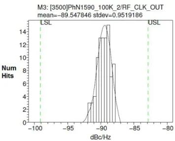
FIGURE 17–RELATABILITY HISTOGRAM OF PHASE NOISE OF A GPS RECEIVER AT 1.59GHZ AT 100 KHZ OFFSET ... 27
FIGURE 18–RELATABILITY HISTOGRAM OF PHASE NOISE OF A GPS RECEIVER AT 1.59GHZ AT 1MHZ OFFSET ... 27
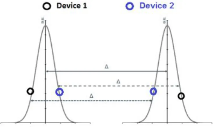
FIGURE 19–DISTRIBUTION OF TWO TEST SHOWING A DIFFERENCE BETWEEN TWO DEVICES ... 28
FIGURE 20–DELTA TEST SHOWING THE DEVICES AS OUTLIERS ... 28
FIGURE 21–BIST MEASUREMENT ACCURACY TO SPECIFICATION SPACE DIAGRAM
... 29
FIGURE 22–A TYPICAL ANALOGUE TEST BUS ... 30
FIGURE 23–A PERFECT ADC RESPONSE ... 43
FIGURE 24–AN ADC RESPONSE WITH ERRORS ... 43
FIGURE 25–AN ADC RESPONSE WITH OFFSET AND GAIN ERROR ... 43
FIGURE 26–AN ADC RESPONSE WITH LOSS OF RANGE AND CODES ... 44
FIGURE 27–AN ADC RESPONSE SHOWING DIFFERENT INL COMPARISONS ... 45
FIGURE 28–AN ADC HARMONIC SPECTRUM WITH A SINGLE TONE INPUT ... 48
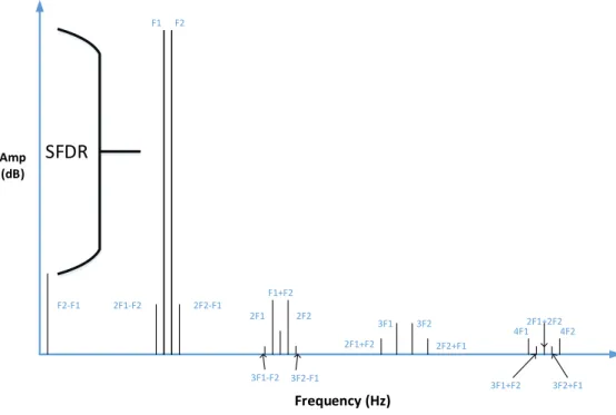
FIGURE 29–AN ADC HARMONIC SPECTRUM WITH A TWO TONE INPUT ... 49
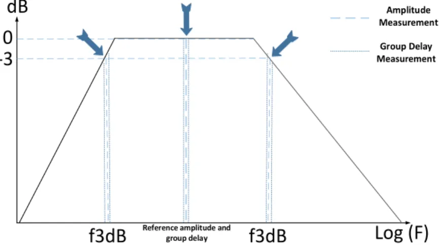
FIGURE 30 – FILTER FREQUENCY RESPONSE SHOWING THE STANDARD MEASUREMENT ANALYSIS ... 52
FIGURE 31–ACONTINUOUS LINEAR CHIRP ... 55
FIGURE 32–TIME DOMAIN OF DISCRETE LINEAR CHIRP ... 55
FIGURE 33–FREQUENCY DOMAIN OF DISCRETE LINEAR CHIRP ... 56
FIGURE 34-TIME DOMAIN OF A DISCRETE STEPPED CHIRP ... 56
FIGURE 35-FREQUENCY DOMAIN OF A DISCRETE STEPPED CHIRP ... 56
FIGURE 36-AMULTITONE WAVEFORM - COMPONENT ... 57
FIGURE 37-AMULTITONE WAVEFORM – COMPOSITE... 57
FIGURE 38–FFT OF COMPOSITE MULTITONE WAVEFORM ... 57
FIGURE 39–ACREST FACTOR REDUCED MULTITONE WAVEFORM ... 58
FIGURE 40–FFT OF CREST FACTOR REDUCED MULTITONE WAVEFORM ... 58
FIGURE 41– FFT OF CREST FACTOR REDUCED 4 TONE MULTITONE WAVEFORM USING H.KITAYOSHI ALGORITHM ... 58
FIGURE 42–FFT OF CREST FACTOR REDUCED 200 TONE MULTITONE WAVEFORM USING H.KITAYOSHI ALGORITHM ... 59
FIGURE 43 – FFT OF CREST FACTOR REDUCED 2000 TONE MULTITONE WAVEFORM USING H.KITAYOSHI ALGORITHM ... 59
FIGURE 42-TEST SETUP OF CHIRP TEST OF FILTERS ... 59
FIGURE 43-PHASE CALIBRATION CIRCUIT ... 63
FIGURE 44–ILLUSTRATION STEPPED CHIRP STEP CREATION –EQUATION (14) ... 66
FIGURE 45–PHASE CHARACTERISTIC OF A LINEAR CHIRP ... 68
FIGURE 46–FREQUENCY DOMAIN REPRESENTATION OF A DISCRETE LINEAR CHIRP ... 69
FIGURE 47–ZOOM IN ON THE CHIRP UPPER SIDELOBE ... 70
FIGURE 48–AMPLITUDE MEASUREMENT DSP CODE ... 71
FIGURE 49-DSP ALGORITHM FLOW FOR 3 DB POINT CALCULATION OF BANDPASS FILTER ... 71
FIGURE 50-TIME DOMAIN CAPTURE THROUGH BANDPASS FILTER ... 73
FIGURE 51-FREQUENCY DOMAIN CAPTURE OF BANDPASS 40 KHZ FILTER ... 73
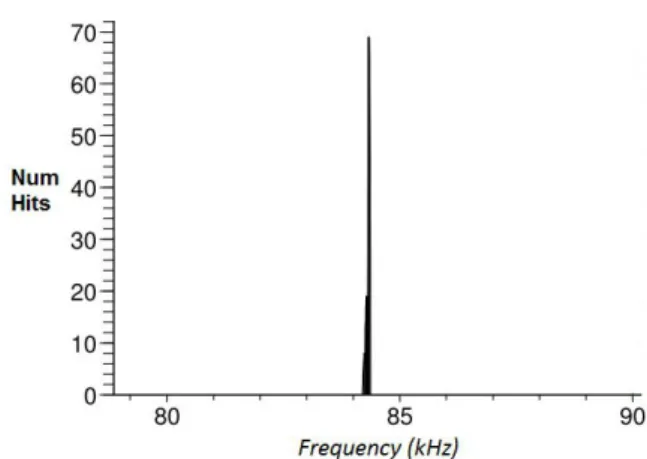
FIGURE 52-FREQUENCY DOMAIN CAPTURE OF 500 KHZ BANDPASS FILTER ... 74
FIGURE 53 -MEASUREMENT STABILITY HISTOGRAM OF THE 40 KHZ BPF FILTER UPPER CUT OFF FREQUENCY ... 75
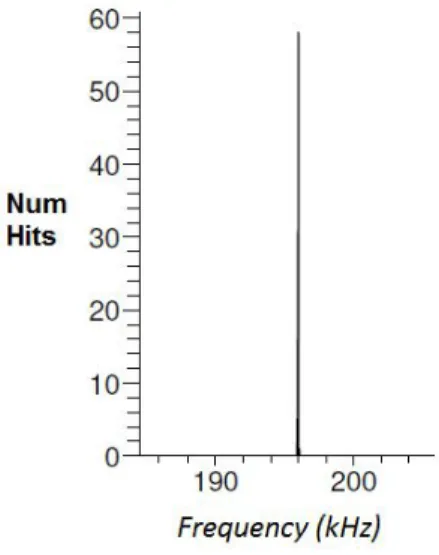
FIGURE 54-MEASUREMENT STABILITY HISTOGRAM OF THE 550 KHZ BPF LOWER CUT OFF FREQUENCY ... 76
FIGURE 55-CAPTURE OF CONTINUOUS WAVEFORM ... 78
FIGURE 56-CAPTURE OF CONTINUOUS WAVEFORM ... 78
FIGURE 57–VECTOR DIAGRAM REPRESENTED AS COMPLEX NUMBERS ... 78
FIGURE 58–TIME MEASUREMENT DSP CODE ... 79
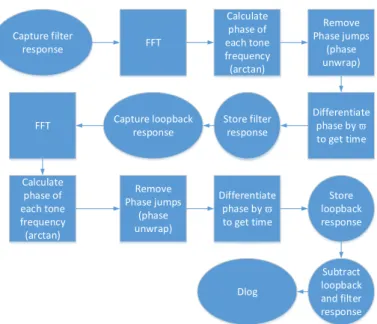
FIGURE 59–GROUP DELAY MEASUREMENT FLOW CHART ... 80
FIGURE 60-PHASE CHANGE OF FILTER WITHOUT PHASE JUMPS REMOVED ... 81
FIGURE 61-PHASE CHANGE OF FILTER ... 81
FIGURE 62-PHASE CHANGE OF REFERENCE ... 81
FIGURE 63-TIME CHANGE OF BOTH OUTPUT OF FILTER AND REFERENCE ... 82
FIGURE 64-GROUP DELAY OF THE FILTER –BAND 1 ... 82 FIGURE 65-REPEATABILITY OF THE GROUP DELAY CHIRP SOLUTION WITH ATE. 84
FIGURE 66-REPRODUCIBILITY OF THE GROUP DELAY CHIRP SOLUTION WITH ATE
... 85
FIGURE 67–RF TESTER SETUP SHOWING THE WEAKNESS WITH CALIBRATING THE FULL RF PATH WHILST TESTING RF TRANSMITTERS. ... 89
FIGURE 68–RF TESTER SETUP SHOWING THE WEAKNESS WITH CALIBRATING THE FULL RF PATH WHILST TESTING RF RECEIVERS. ... 89
FIGURE 69–STANDARD RFTESTER OVERVIEW... 90
FIGURE 70–RFRXBLOCK DIAGRAM ... 90
FIGURE 71 –FREQUENCY SPECTRUM OF A CHIRPED RF SOURCE WITHOUT QUADRATURE SIGNAL ON THE IQ INPUTS. ... 92
FIGURE 72–FREQUENCY MIXER SCHEMATIC DIAGRAM ... 92
FIGURE 73–DISCRETE LINEAR CHIRP USED IN RX MODEL SIMULATION ... 95
FIGURE 74–SIMULATED RF CHIRP MODULATION SIGNAL ... 95
FIGURE 75 –SIMULATED AMPLIFIED RF CHIRP MODULATION SIGNAL, WITH DISTORTION, COMPARED TO NON-DISTORTED SIGNAL ... 95
FIGURE 76 –DISTORTED DOWNCONVERTED CHIRP SIGNAL VS NON DISTORTED DOWNCONVERTED SIGNAL ... 96
FIGURE 77 –DISTORTED DOWNCONVERTED CHIRP SIGNAL VS LOW PASSED DISTORTED DOWNCONVERTED SIGNAL ... 96
FIGURE 78 –DISTORTED DOWNCONVERTED CHIRP SIGNAL VS NON DISTORTED DOWNCONVERTED SIGNAL ... 96
FIGURE 79–SIMULATED DISTORTED CHIRP SIGNAL COMPARED TO NON-DISTORTED VERSION ... 98
FIGURE 80–GROUP DELAY THROUGH THE MODELLED RX UNDER THE INFLUENCE OF DISTORTION ... 98
FIGURE 81 –SIMULATED INCREASE OF THE 11TH ORDER PRODUCT OF THE DOWNCONVERTER DISTORTED CHIRP SIGNAL COMPARED TO SMOOTHED VERSION. .. 98
FIGURE 82 –SIMULATED CHIRP SIGNAL WITH BANDWIDTH GREATER THAN BANDPASS FILTER... 99
FIGURE 83–GROUP DELAY PLOT OF 20 ORDER BANDPASS FILTER ... 100
FIGURE 84–GROUP DELAY PLOT OF 20 ORDER BANDPASS FILTER MEASURED AT DOWNCONVERTED FREQUENCY USING CHIRP SWEEP ... 100
FIGURE 85 –GROUP DELAY DIFFERENCE PLOT OF TWO, 20 ORDER BANDPASS
FILTER WITH CORNER FREQUENCY DIFFERENCES OF 1%... 100 FIGURE 86 –GROUP DELAY DIFFERENCE PLOT OF TWO, 20 ORDER BANDPASS
FILTER WITH CORNER FREQUENCY DIFFERENCES OF 1% ... 101 FIGURE 87–RFGROUP DELAY MEASUREMENT FLOW CHART ... 101 FIGURE 88–DIAGRAM OF RFMEASURE PORT MODULE ... 103 FIGURE 89 –DIAGRAM OF IQ WAVEFORMS WITH 0 AND 90 DEGREES (/2) PHASE SHIFT ... 105
FIGURE 90–RFGENERATOR WITH IQ MODULATION ... 105 FIGURE 91 –DSB-SC CHIRP MODULATION WAVEFORM AT 500 MHZ CARRIER FREQUENCY ... 106
FIGURE 92–RAW CAPTURE OF CHIRP SIGNAL FROM RFMEASURE PORT ... 107 FIGURE 93–EXTRACTED DATA FROM RAW CAPTURE ... 107 FIGURE 94 –DEMODULATED DSB CHIRP MODULATION WAVEFORM CENTRED AT THE MAX FREQUENCY OF THE CHIRP ... 107
FIGURE 95 –PHASE RESPONSE OF CAPTURED RF CHIRP VS EXPECTED RFCHIRP
... 109 FIGURE 96 –ZOOM IN OF THE MEASURED GROUP DELAY PROFILE OF THE MEASUREMENT VS EXPECTED PROFILE USING A CHIRP SIGNAL ... 109
FIGURE 97–GROUP DELAY OF XCERRA RF MEASURE PORT. ... 109 FIGURE 98 –MEASUREMENT ERROR OF GROUP DELAY OF IF PATH OF THE RF
MEASURE PORT. ... 110 FIGURE 99–GROUP DELAY OF 10MHZ LPF IN THE IF PATH OF THE XCERRA RF MEASURE PORT ... 111 FIGURE 100–GROUP DELAY OF 1MHZ BPF IN THE IF PATH OF THE XCERRA RF MEASURE PORT ... 112 FIGURE 101–GROUP DELAY OF 2MHZ BPF IN THE RF PATH OF THE XCERRA RF MEASURE PORT. ... 112
FIGURE 102-SPECTRUM OF 2-SIGNAL INTERLEAVED 3RD HARMONICS SUPPRESSED SIGNAL ... 120
FIGURE 103 - SPECTRUM OF 4-SIGNAL INTERLEAVED 2ND & 3RD HARMONIC SUPPRESSED SIGNAL ... 120
FIGURE 104-AWG TO DIGITIZER LOOPBACK ... 121 FIGURE 105-MEASURED SPECTRUM LEVEL IMPROVEMENT OF THE REFERENCE VS SUPPRESSED 2ND HARMONIC FOR AWG. ... 122
FIGURE 106-MEASURED SPECTRUM LEVEL IMPROVEMENT OF THE REFERENCE VS.
SUPPRESSED 3RD HARMONIC FOR AWG. ... 122 FIGURE 107 - COMPARISON OF 3RD HARMONIC WHEN BOTH 3RD AND 5TH
HARMONICS ARE SUPPRESSED FOR AWG. ... 123 FIGURE 108 - COMPARISON OF 5TH HARMONIC WHEN BOTH 3RD AND 5TH
HARMONICS ARE SUPPRESSED FOR AWG. ... 124 FIGURE 109-TESTER SETUP WITH ADC ... 125 FIGURE 110-SPECTRUM OF 16-BIT ADC WITHOUT SUPPRESSION ... 126 FIGURE 111-SPECTRUM OF 16-BIT ADC WITH 2ND HARMONIC SUPPRESSED ... 126 FIGURE 112 -REPEATABILITY OF THD ON SITE 1 OF THE 12-BIT ADC EXAMPLE
... 129 FIGURE 113 -REPEATABILITY OF THD ON SITE 2 OF THE 12-BIT ADC EXAMPLE
... 129 FIGURE 114 - SIMULATION OF CONVENTIONAL TWO-TONE GENERATION VS 2-
SIGNAL INTERLEAVED IMD3 SUPPRESSION TECHNIQUE ... 137 FIGURE 115 - SIMULATION OF CONVENTIONAL TWO-TONE GENERATION VS 2-
SIGNAL INTERLEAVED IMD5 SUPPRESSION TECHNIQUE ... 137 FIGURE 116 – SIMULATION OF CONVENTIONAL TWO-TONE GENERATION VS 2-
SIGNAL INTERLEAVED IMD4 SUPPRESSION TECHNIQUE ... 138 FIGURE 117 - SIMULATION OF CONVENTIONAL TWO-TONE GENERATION VS 2-
SIGNAL INTERLEAVED IMD3 SUPPRESSION TECHNIQUE WITH ONLY 7TH ORDER NON-
LINEARITY. ... 138
FIGURE 118 - SIMULATION OF CONVENTIONAL TWO TONE GENERATION VS 4-
SIGNAL INTERLEAVED IMD4,5 SUPPRESSION TECHNIQUE ... 141 FIGURE 119- DISTORTION AND SUB NYQUIST COMPONENTS OF 2-SIGNAL PHASE SWITCHING ... 143
FIGURE 120- DISTORTION AND SUB NYQUIST COMPONENTS OF 4-SIGNAL PHASE SWITCHING ... 143
FIGURE 121-ARCHITECTURE OF AN INTERPOLATING DAC ... 144 FIGURE 122-FREQUENCY DOMAIN OF A TWO TONE SIGNAL UP SAMPLED BY 2. . 146 FIGURE 123-4X UPSAMPLED VERSION OF 4-SIGNAL PHASE SWITCHING ... 146 FIGURE 124-4-SIGNAL PHASE SWITCHED,2 TWO TONE SIGNALS, UP SAMPLED X2 ... 146 FIGURE 125-FIR WITH 4X INTERPOLATION, USED TO FILTER 2X UP SAMPLING . 147 FIGURE 126-4-SIGNAL PHASE SWITCHED SIGNAL WITH DISTORTION, UP SAMPLED X2 AND FIR FILTER INTERPOLATED BY 4, 2X UP SAMPLING FILTERED, INSERTED ZEROS SMOOTHED ... 147
FIGURE 127 - INTERPOLATION PROCESS EFFECT ON BOTH STANDARD AND 3RD
SUPPRESSED PHASE SWITCHED SINEWAVE ... 147 FIGURE 128-INTERPOLATION PROCESS EFFECT ON BOTH STANDARD AND 4TH,5TH
SUPPRESSED PHASE SWITCHED SINEWAVE ... 148 FIGURE 129 – IMD3 DEGRADATION CAUSED BY SUPPRESSING 3RD ORDER TONES
... 150 FIGURE 130-IMD5 DEGRADATION CAUSED BY SUPPRESSING 5TH ORDER TONES150 FIGURE 131-IMD4 SUPPRESSION REDUCING 3RD AND 5TH ORDER TONES ... 150 FIGURE 132 - IMD3, 5, 7, REDUCTION USING 4TH & 5TH ORDER 4-SIGNAL INTERLEAVED SUPPRESSION TECHNIQUE ... 151
FIGURE 133 - THE EFFECT OF ADDING A STARTING PHASE TO AN 4TH ORDER SUPPRESSION ON THE IMD3 TONES ... 152
FIGURE 134-EFFECT OF ADDING A STARTING PHASE TO A 4TH ORDER SUPPRESSION ON THE IMD5 TONES ... 152
FIGURE 135-EFFECT OF ADDING A STARTING PHASE TO A 4TH ORDER SUPPRESSION ON THE IMD7 TONES ... 153
FIGURE 136-COMPARISON OF 4-SIGNAL INTERLEAVING SUPPRESSION TECHNIQUE ON TWO AWG’S WITHIN THE SAME TEST SYSTEM ... 154
FIGURE 137–IMD3 OF SUPPRESSION VS PHASE AND FREQUENCY ... 155 FIGURE 138–IMD5 SUPPRESSION VS PHASE AND FREQUENCY ... 155 FIGURE 139–IMD7 SUPPRESSION VS PHASE AND FREQUENCY ... 156 FIGURE 140 – REPEATABILITY MEASUREMENT OF IMD3 USING STANDARD SINEWAVE WITH ADDED STARTING PHASE. ... 156
FIGURE 141 –DEGRADATION OF IMD3 PERFORMANCE ACROSS PHASE OF STANDARD SINEWAVE VS IMD3 SUPPRESSED VERSION ... 157
FIGURE 142 –IMPROVEMENT OF IMD3 PERFORMANCE ACROSS PHASE OF STANDARD SINEWAVE VS WAVEFORM WITH IMD4 AND IMD5 SUPPRESSED ... 157
FIGURE 143 –IMPROVEMENT OF IMD5 PERFORMANCE ACROSS PHASE OF STANDARD SINEWAVE VS WAVEFORM WITH IMD4 AND IMD5 SUPPRESSED ... 157
FIGURE 144 –IMPROVEMENT OF IMD7 PERFORMANCE ACROSS PHASE OF STANDARD SINEWAVE VS WAVEFORM WITH IMD4 AND IMD5 SUPPRESSED ... 158
FIGURE 145–INTERMODULATION DISTORTION PRODUCTS SEEN BY ADC CAUSED BY POOR PERFORMANCE OF AWG. THIS IS NOT THE REAL PERFORMANCE OF THE
ADC. ... 159 FIGURE 146–REAL INTERMODULATION DISTORTION PERFORMANCE OF ADC DUE TO IMPROVING THE PERFORMANCE OF THE INTERMODULATION DISTORTION OF THE
AWG. ... 160 FIGURE 147 –GRAPHICAL REPRESENTATION OF HOW DEVICE PERFORMANCE METRICS SHIFT WITH TEMPERATURE AND HOW GUARDBANDS ARE APPLIED AT THE STANDARD TEST TEMPERATURE TO GUARD AGAINST THESE FAILURES ENTERING THE FIELD ... 163
FIGURE 148-WAFERMAP OF INITIAL WAFER PROBE OTP SCREEN AT -40 DEG @2.2 V ... 163 FIGURE 149–BLOCK DIAGRAM OF THE DEVICE ... 164
FIGURE 150-WAFER-MAP OF MULTIPLE -40 DEG FAILURES @2.2V ... 166 FIGURE 151-WAFERMAP SHOWING OTP FAILURES AT 35 DEG @2V– STEP FIELD
... 166 FIGURE 152 - SCHEMATICS OF DIFFERENT CONDITIONS OF GATE-OXIDE BREAKDOWN ANTI-FUSE ... 168
FIGURE 153 - DIAGRAM SHOWING THE PROGRAMMED CURRENT SHIFTS WRT TEMPERATURE ... 168
FIGURE 154-OLD NWELL TO NEW NWELL PROCESS WINDOW ... 169 FIGURE 155 - ELECTRONIC INKING OF SUSPECT NEIGHBOUR DIE OF STEP FIELD WAFER ... 170
FIGURE 156--40 FAILURE @2.2V FOR CORRELATION AGAINST VOLTAGE AT 35
DEG ... 171 FIGURE 157--40 FAILURE FAILING AT 35 DEG @1.8V ... 171 FIGURE 158- -40 DEG FAILURE PASSING AT 35 DEG @1.825V ... 172 FIGURE 159- WAFERMAP OF A STEP FIELD WAFER FULLY TESTED AT -40 DEG @ 2.2V ... 172 FIGURE 160-WAFERMAP OF A STEP FIELD WAFER TESTED AT 35 DEG @1.8V . 172 FIGURE 161-NEW NEAREST NEIGHBOR INKING STRATEGY ... 173 FIGURE 162--40 DEG PROBE WITH NEW NWELL DESIGNED OTP CELL @2.2V . 175 FIGURE 163-35 DEG VERY LOW VOLTAGE SCREEN @1.8V ... 175 FIGURE 164 - PLOT OVER TIME SHOWING THE IMPROVEMENT IN THE PRODUCT YIELD ... 175
FIGURE 165-STACKED MAP OF FAILING DIE OVER 30 LOTS –15 DEVICES IN 4.6M– 3PPM ... 177 FIGURE 166 -ELECTRICAL EQUIVALENT CIRCUIT, LAYOUT, AND TEM IMAGE OF THE EEPROM BIT CELL. ... 180
FIGURE 167 -LABORATORY TEST EQUIPMENT FOR EEPROM BIT CELL FAST BIT TESTING ... 181
FIGURE 168-SCHEMATIC DIAGRAM OF THE DIFFERENTIAL BIT CELL CONCEPT AND THE SENSE AMPLIFIER. ... 181
FIGURE 169 - FULLY DIFFERENTIAL SENSE AMPLIFIER SCHEMATIC. RED LINE:
CURRENT PATH IN SENSE AMPLIFIER MODE FOR DATALINE.GREEN LINE: CURRENT PATH IN EXTERNAL CELL CURRENT MEASUREMENT MODE FOR DATALINEB. ... 182
FIGURE 170-MINIMUM VOLTAGE TO ERASE ALL BIT CELLS FOR EACH DEVICE ON ONE WAFER ... 185
FIGURE 171-PROGRAMMING PROFILE OF EEPROM BIT CELL ... 185 FIGURE 172–FULL PROGRAMMING PROFILE OF EEPROM BIT CELL ... 186 FIGURE 173–16-SITE EEPROM WAFER SORT PROBE HEAD ... 187 FIGURE 174 - BINFLIP REPORT WITH FAIL TO PASS FLIPS OF EEPROM CORNER WAFER ... 188
FIGURE 175 - WAFER EXHIBITING A STEP FIELD REPORTED BY COST OPTIMIZED TEST PROGRAM ... 190
FIGURE 176 - WAFER MAP OF STEP FIELD WAFER WITH THE ORIGINAL TEST PROGRAM ... 191
FIGURE 177-WAFER MAP OF AN EEPROM SHOWING ABNORMAL FAIL PATTERN
... 192 FIGURE 178-WAFER MAP OF AN EEPROM SHOWING RANDOM DISTRIBUTED FAST
EEPROM BIT CELLS (RED DOTS). ... 192 FIGURE 179-TUXQBDWAT MEASUREMENT RESULTS OF MAVERICK LOT.(LSL
LOWER SPECIFICATION LIMIT). ... 193 FIGURE 180-DRAIN SOURCE CURRENT DISTRIBUTION OF THE EEPROM BIT CELLS ACROSS THE LOT. ... 193
FIGURE 181-DRAIN SOURCE CURRENT WAFER MAP OF THE EEPROM BIT CELLS. ... 195 FIGURE 182 - BIT CELL CURRENT DISTRIBUTION (PROGRAMMED CELL) OF A TYPICAL LOT. ... 195
FIGURE 183 - BIT CELL CURRENT DISTRIBUTION (PROGRAMMED CELL) OF THE MAVERICK LOT ... 195
FIGURE 184-WAFER MAP OF THE EEPROM BIT CELL CURRENT TEST ... 197 FIGURE 185 - WAFER MAP OF FAST EEPROM BIT CELLS TESTED WITH THE OPTIMIZED FAST BIT TEST (RED DOTS). ... 198
FIGURE 186 - WAFER MAP OBTAINED WITH OPTIMIZED PRODUCTION TEST PROGRAM. ... 198
FIGURE 187-WAFER MAP OF AN EEPROM SHOWING ABNORMAL FAIL PATTERN
... 198 FIGURE 188- ENDURANCE BEHAVIOR OF NVMS BASED ON FOWLER-NORDHEIM TUNNELING ... 201
FIGURE 189-ERASE CYCLE CLASS VOLTAGE DISTRIBUTION ... 204 FIGURE 190-PROGRAM CYCLE CLASS VOLTAGE DISTRIBUTION ... 204 FIGURE 191-SOFT ERASE SCREENING BASED ON 1 SOFT ERASE PULSE ... 206 FIGURE 192-SOFT PROGRAM SCREENING BASED ON 1 SOFT PROGRAM PULSE ... 206 FIGURE 193–DEFECT DENSITY OF THE AMS 0.35 UM CMOS PROCESS ... 209 FIGURE 194–DYNAMIC HIGH VOLTAGE STRESS DIGITAL TIMING DIAGRAM ... 213 FIGURE 195–ENHANCED HIGH VOLTAGE STRESS DIGITAL TIMING DIAGRAM .... 213 FIGURE 196–DIAGRAM OF HOW DPAT DYNAMICALLY CHANGES TEST LIMITS TO REMOVE OUTLIERS ... 215
FIGURE 197–POWER OF DPAT TO REMOVE SUSPICIOUS OUTLIERS ... 215 FIGURE 198–WAT TO WAFER SORT DATA CORRELATION ... 216 FIGURE 199 – WAT TO ANALOGUE PARAMETER ESTIMATION FOR PREDICTING OPTIMUM TRIM CODES ... 218
FIGURE 200–1687.2A STANDARDISED ANALOGUE TEST BUS INSERTION ... 219
L IST OF A BBREVIATIONS AND A CRONYMS
ADC - Analogue to Digital Converter AIAG - Automotive Industry Action Group AIMI - Analogue Infant Mortality Inducing APQP - Advanced Product Quality Planning ATB - Analogue Test Bus
ATE - Automated Test Equipment
ATPG - Automated Test Pattern Generation AWG - Arbitrary Waveform Generator
BB - BaseBand
BIF - Built-In Function BIST - Built-In Self-Test BOST - Built-Out Self Test BPF - Band Pass Filter
CMOS - Complementary Metal Oxide Semiconductor CPK - Process Capability
CUT - Circuit Under Test
DAC - Digital to Analogue Converter DIB - Device Interface Board
DAB - Digital Audio Broadcast DC - Direct Current
DFT - Design For Test
DFT - Discrete Fourier Transform DNL - Differential Non-Linearity DPAT - Dynamic Part Averaging Testing DPPB - Defect Parts Per Billion
DPPM - Defect Parts Per Million DOT - Defect Orientated Test
DSB-SC - Double Sideband, Suppressed Carrier DSP - Digital Signal Processing
DUT - Device Under Test
EDA - Electronic Design Automation
EEPROM - Electrical Erasable Read Only Memory EEHVOX - EEPROM High Voltage Oxide
ENOB - Effective Number of Bits EVM - Error Vector Magnitude FG - Floating Gate
FFT - Fast Fourier Transform FMEA - Failure Mode Effect Analysis FSR - Full Scale Range
GPS - Global Positioning by Satellite
GRR - Gauge Repeatability and Reproducibility HF - High Frequency
HV - High Voltage
HPF - High Pass Filter
IATF - International Automotive Task Force IC - Integrated Circuit
ICL - Instrument Control Language
IEEE - Institute of Electrical and Electronic Engineers IF - Intermediate Frequency
IMD - Intermodulation Distortion
IO - Input Output
IoT - Internet of Things
IDM - Integrated Device Manufacture IP - Intellectual Property
IPOX - Inter Poly Oxide
ISI - Inter Symbol Interference JTAG - Joint Test Action Group LNA - Low Noise Amplifier INL - Integral non-linearity LPF - Low Pass Filter
IDM - Independent Device Manufacture LO - Local Oscillator
LSB - Least Significant Bit LSI - Large Scale Integration LSL - Lower Specification Limit MIMO - Multiple-Input Multiple-Output MRB - Material Review Board
MSB - Most Significant Bit
NBTI - Negative Bias Temperature Instability NCO - Numerically Controlled Oscillator NFC - Near Field Communications NMOS - N-type Metal Oxide Semiconductor NVM - Non-Volatile Memory
OS - Operating System
OTP - One Time Programmable PAT - Part Average Testing
PDL - Procedural Description Language PMOS - P-type Metal Oxide Semiconductor PPAP - Production part approval process
PPB - Parts per Billion PPM - Parts Per Million PPT - Parts Per Trillion
PSW - Part Submission Warrant QA - Quality Assurance
QAM - Quadrature Amplitude Modulation QBD - Charge to Breakdown
QPSK - Quadrature Phase Shift Keying RADAR - Radio Detection and Ranging R&D - Research and Development
RAM - Random Access Memory
RMA - Return Material Advice RMS - Root Mean Square RF - Radio Frequency RFSOC - RF System on a Chip
RX - Receiver
ROM - Read Only Memory
SAR - Synthetic Aperture RADAR
SAR - Successive Approximation Register SFDR - Spurious Free Dynamic Range SINAD - Signal to Noise and Distortion SLM - Scribe Line Monitor
SNR - Signal to Noise Ratio SPI - Serial Peripheral Interface SOC - System on a Chip
SPST - Single Pole Single Throw SPDT - Single Pole Double Throw
TEM - Transmission Electron Microscope TETRA - Terrestrial Trunked Radio
TCXO - Temperature Controlled Crystal Oscillator TG - Transmission Gate
THD - Total Harmonic Distortion ToF - Time of Flight
TSP - Time Stretched Pulse TUX - Tunnel Oxide
TX - Transmitter
uP - Microprocessor
UHF - Ultra High Frequency USL - Upper Specification Limits UTP - Unit Test Period
UWB - Ultra Wideband
VGA - Variable Gain Amplifier VHF - Very High Frequency VLV - Very Low Voltage WAT - Wafer Acceptance Test WRT - With Respect to
L IST OF A PPENDICES
APPENDIX 1-RFANALOGUE MIXED SIGNAL BLOCK DIAGRAM ... 236 APPENDIX 2-PRODUCTION TESTER ... 237 APPENDIX 3–IDDQ ANALOGUE DATALOG ... 238 APPENDIX 4–ECL DIVIDER REFERENCE CLOCK CIRCUITRY ... 240 APPENDIX 5-OTPPRODUCTION TEST FLOW ... 241 APPENDIX 6-PRODUCTION PROBER AT -40 DEGREES ... 242 APPENDIX 7 – YIELD OF EEPROM PRODUCT FROM AMS 0.35 UM SILICON FOUNDRY ... 243
APPENDIX 8–AUTHORS INDIVIDUAL CONTRIBUTIONS ... 244
1 I NTRODUCTION
The semiconductor business is at a junction where the required quality level of products is increasing at an exponential rate, whereas the test cost per device is being driven lower. More stringent quality requirements are the result of the concentration on market penetration for one product rather than multiple different products and hence the volume of any one-semiconductor device increases at the same rate as the acceptance of individual products into the market. A simple example of this is the cell phone market.
10 years ago, Nokia had several tens of mobile phones for sale at any one time and for each of these products there could have been several different suppliers of the same device function for each model of phone. In today’s world, the old guard of manufacturers has failed to adapt to changing market conditions and the available choices to the consumer is a simple one between Apple and Samsung. As the market is growing at 5 % year on year, and as the market segment has shrunk to two models of phone it is obvious that the volume of the equivalent devices that once went into the Nokia has had a more than a 10-fold increase. Whilst quality levels have actually decreased in some cases, more returns have been received from end customers, for analysis by the semiconductor providers. Therefore, without significantly increasing quality assurance personnel, semiconductor providers would be at a loss to deal with this changing environment.
One way of dealing with the need to drive down the dppm in the field is by introducing more stringent testing at the backend of the semiconductor manufacturing flow. In the automotive business segment, it has long been the requirement to test every specification detailed in the datasheet at the test stage, together with the need to launch a
ANALOGUE MIXED SIGNAL TEST DEVELOPMENT
2 Peter Sarson - December 2018
product into production in a safe launch mode where the product is tested at the temperature extremes with a characterisation style test program. However, this is extremely costly in terms of test time and the delivery times of such products are very long due to the throughput rates. In recent years, a trend has emerged where such automotive style backend test flows, are being demanded by the high volume device consumers simply due to the volume they are expecting. From an automotive point of view, the need is due to safety concerns. From a mobile phone manufacturer’s viewpoint, if the product has a quality level of 100 ppm and 1 billion devices are expected per year, this would lead to a return rate of 100 thousand units per year.
Simply put, this would be prohibitively expensive for the end consumer in rework and would require a Quality Assurance (QA) department of a company to be enormous to deal with so many returns per year.
In contrast with the above, there is the added pressure on test development to significantly decrease test times of products because of the overall cost of semiconductor devices. This is due to Moore’s law which states that every 18 months there will be a reduction in process geometry size of 50 %, thus leading to the ability to produce twice as many parts one year compared to the last resulting in significantly cheaper semiconductor manufacturing year on year. In digital test development there has been somewhat of a drive to keep up with Moore’s law in that more defects are being found as a result of more and more efficient ways of capturing them, using such test technique as scan, IDDq, cell aware etc. Unfortunately, in the analogue space, no such progression has been made and as such analogue mixed-signal test development is still in its infancy; therefore, with the pressures of the modern world cracks are becoming apparent. As process nodes shrink, it is becoming increasingly difficult to predict the type of random defects that have been standard within the semiconductor business using larger geometries. Hence increasing the pressure for the backend to find such issues efficiently and cost effectively. However, this is in stark contrast to reality.
As the world of IoT starts to develop, from 2018 to 2023, the number of analogue devices shipped worldwide is predicted to grow by some 11 %; this is estimated to be approximately 250 billion devices. This will further increase the pressure to decrease test time from a throughput point of view. There is only so much space for testers without building new facilities or outsourcing to external subcontractor manufacturers.
However, unless a company wishes to invest heavily in quality assurance personnel, the
quality level of these parts needs to increase at the same percentage as the growth otherwise the level of returns coming from the field will simply be overwhelming. For a small company, this could be the difference between the success and failure of the venture.
The silicon foundries around the world are at a loss as to further decrease the number of defects per square millimetre, therefore the only option left to increase the quality level is somehow to force the latent defects to be 100 % detectable. There has been a lot of effort given to producing devices in the massive parallel testing space but this is only feasible for devices that are constantly running production, as the setup times of such systems are too high for medium volume products. Simply stated, it would take longer to setup the system; than it would take to test the amount of required devices.
What is needed is a way of testing devices that captures a specification based failure but at the same time is able to detect a latent defect that would fail in the field. For example, if such a device was in a safety critical system within an autonomous vehicle it could potentially kill the passenger.
This is a momentous task and it cannot be achieved solely from one element of the semiconductor process flow but needs a combined effort from all sides of the process.
There has been much work done in both academia and industry to tackle these issues but usually only one aspect is addressed at any one time, and as a whole, the solutions that are produced do not work for similar companies, as the solutions may not take into account everything earlier or later in the process flow. This also leads to the lack of adoption of such solutions, or even, the will to look at these issues as the solution is simply not transparent.
Many areas can be addressed, in both design and the test world to help drive this process forward. However, a certain arrogance from design has been observed, it can be seen that it is believed that test is a simple discipline, and design is more important. This type of thinking is very common in the industry and can be observed simply by looking at the test time of a product. It can be seen that there is a strong correlation between a device that had a very strong collaboration and an efficient backend test process.
However this requires to go one step further; the way a device is designed or even laid out can influence whether a certain defect can be detected or not. In many cases, analogue fault coverage can be as low as 40 % of the possible defects that can occur.
However as the industry states that there is 100 % coverage because specifications are