PAPER
Special Section on Reconfigurable SystemsAutomatic Generation Tool of FPGA Components for Robots
Takeshi OHKAWA†a),Member, Kazushi YAMASHINA†, Takuya MATSUMOTO†,Nonmembers, Kanemitsu OOTSU†,andTakashi YOKOTA†,Members
SUMMARY In order to realize intelligent robot system, it is required to process large amount of data input from complex and different kinds of sensors in a short time. FPGA is expected to improve process performance of robots due to better performance per power consumption than high per- formance CPU, but it has lower development productivity than software.
In this paper, we discuss automatic generation of FPGA components for robots. A design tool, developed for easy integration of FPGA into robots, is proposed. The tool named cReComp can automatically convert circuit written in Verilog HDL into a software component compliant to a robot software framework ROS (Robot Operation System), which is the standard in robot development. To evaluate its productivity, we conducted a sub- ject experiment. As a result, we confirmed that the automatic generation is effective to ease the development of FPGA components for robots.
key words: FPGA, component oriented development, automatic genera- tion, ROS, ROS-compliant FPGA component, robot
1. Introduction
Since autonomous mobile robots need to perform various kinds of processing such as control of several sensors and image processing[1], a high-performance hardware plat- form is required. To drive these robots according to var- ious environment regardless of whether they are outdoors or indoors, wireless communication and battery operation are preferable[2]. In order to process complex performance of autonomous mobile robots, high-performance general- purpose CPU are commonly used for hardware platforms mounted on them, however, their power dissipations are high. Therefore, FPGA (Field Programmable Gate Ar- ray) is expected as a hardware platform for realizing high- performance processing at high-energy efficiency[3].
In general, application development of FPGA is done by RTL (Register Transfer level) using HDL (Hardware De- scription Language), so development productivity is low.
Recently, HLS (High-Level Synthesis) has become useful for generating HDL circuit from software language like C language, however, development of a high-performance cir- cuit using HLS still needs expertise knowledge of FPGA.
Also, in the FPGA, the specifications of the input and out- put (I/O) differ between the chip and the board, so portabil- ity and reusability are significantly inferior compared with software. Therefore, the processing in the hardware imple-
Manuscript received July 27, 2018.
Manuscript revised December 4, 2018.
Manuscript publicized March 1, 2019.
†The authors are with Utsunomiya University, Utsunomiya- shi, 321–8585 Japan.
a) E-mail: [email protected] DOI: 10.1587/transinf.2018RCP0004
mented on the FPGA is characterized by high development cost and low reusability.
On the other hand, in wide field of robot engineering, it is not realistic to grasp all the specialized fields in robot development where there are many necessary technologies.
Therefore, component-oriented development[4] is recog- nized as an effective development method for improving robot development productivity. Component-oriented de- velopment means that processing and functions in a robot are implemented as software components, and a robot sys- tem is constructed by combining components. By the reusability in component-oriented development, develop- ment productivity shall be greatly improved since the de- velopers can focus on advanced features of a robot.
We have proposed ROS-compliant FPGA compo- nent[9]in order to handle any FPGA processing circuit eas- ily in robot systems. ROS (Robot Operating System)[4]–
[6]is a kind of software platform that supports component- oriented development. By using ROS-compliant FPGA component, FPGA can be easily introduced to robots and reusability of FPGA circuits can be improved. However, the development of ROS-compliant FPGA component needs software/hardware co-design and verification so that the de- sign productivity of the communication path is very low.
In this paper, we propose a design support tool for com- ponentization of any FPGA, in order to improve develop- ment productivity of ROS-compliant FPGA component. We named the tool cReComp. It is a design support tool which convers any target circuit (user logic) into a component by giving simple specification definition for data transfer. By using cReComp, it is expected to develop ROS-compliant FPGA components easily even without FPGA development experience.
Contributions of this paper are:
• Discussion about development of FPGA component for robots
• Proposal of the component generation tool named cRe- Comp and its detailed explanation
• Evaluation in terms of design productivity
Compared to our previous work[7], this paper explains im- plementation of cReComp in detail. And compared to our previous technical report[8], this paper describes detailed background and design concept.
After this introduction, we state the issues in develop- ment of FPGA component for robots in Sect. 2. The automa- Copyright c2019 The Institute of Electronics, Information and Communication Engineers
tion tool cReComp for ROS-compliant FPGA component is described in Sect. 3. In Sect. 4, we discuss the evaluation results of the subject experiments in terms of design pro- ductivity. Then, we state about related research in Sect. 5.
The paper concludes in Sect. 6.
2. Issues of FPGA Component for Robots
In this section, FPGA component for robots is discussed.
Next, ROS-compliant FPGA component is briefly de- scribed, which is used to introduce FPGA into robot soft- ware systems easily by publish/subscribe data communi- cation. And the issues concerning the development of the FPGA component is pointed out.
2.1 FPGA Component Technology for Robots
FPGA is expected[3] as not only a high-throughput pro- cessing at cloud servers but also an edge-processing plat- form for energy efficient processing. Promising examples of the edge-processing applications are image recognition, security or quick sensor data processing (sensor fusion) for robots, and so on. However, for software engineers, it is dif- ficult to handle circuit description of FPGA, as it is not easy to design data transfer necessary for performing arbitrary processing. Recently, Programmable SoC is commercially available. Programmable SoC is an LSI chip which equips with microprocessor (CPU) and FPGA logic. For example, Xilinx Zynq-7000 series[13]is a LSI chip with ARM pro- cessor and FPGA. Programmable SoC is expected to ease the use of FPGA circuit by packaging FPGA and ARM pro- cessor for software engineers.
However, even if a programmable SoC is used, data transfer between CPU and FPGA uses off-chip memory, which is not on the programmable SoC. So, in addition to having a deep knowledge of the bus system of CPU-FPGA, an HDL memory access description for data transfer is nec- essary. Besides, the low abstraction level of the description for input/output data from software to the user logic on the FPGA is also one of the factors of lowering development productivity.
Consequently, we would like to improve the reusability of the circuit description on the FPGA by adding an inter- face that makes it easy to transfer data between the CPU and the FPGA. There are many options of letting FPGA have an interface to software. Furthermore, by complying with the communication model provided by ROS (Robot Operating System), which is going to be described in the next subsec- tion, the application of FPGA can be treated as a component in ROS.
2.2 ROS (Robot Operating System)
ROS (Robot Operating System)[4] is a software plat- form that supports component-oriented development for robots[5]. ROS provides a build tool for application soft- ware for robots and a framework for software to communi-
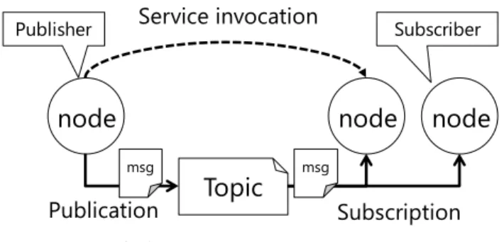
Fig. 1 ROS system concept overview
cate with each other as an open source. In ROS, there are so many usable software assets, and in the official ROS repos- itory more than 3,000 packages are registered as of January 2017[6].
In ROS, when a robot system is constructed, it is pos- sible for developers to introduce components which they wish to use into their systems, so they can use the compo- nents easily. That is to say, it is easy to add components to their own system. Such system enhance-ability and scal- ability is realized by a communication framework in ROS.
Figure 1 shows the communication model of ROS. In ROS, one executable file is called “node”, and there are two kinds of communication methods between nodes. The first one is called “ROS service”, and nodes carry out synchronous communication of general server/client system. The second one is called “publish-subscribe messaging”, which is asyn- chronous data communication. When several nodes com- municate in the ROS system, a sender of the data (pub- lisher) queues a message to a communication channel called
“topic”. A message is a data format of ROS that enables a developer to use any data structure. After receiving data from a publisher node, a subscriber node subscribes to a spe- cific topic, and receives data when there is an update in the message in the topic.
2.3 ROS-Compliant FPGA Component
When a robot system is constructed by using ROS, pub- lish/subscribe messaging is often used, and by using such a communication model, it is possible to carry out data com- munication easily. Therefore, attach/detach of components to/from the system can be also easily realized.
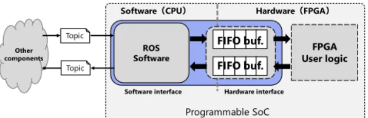
ROS-compliant FPGA component[9] is a framework of hardware/software (HW/SW) for easy introduction of a processing circuit (application) operating on an FPGA to a robot system using ROS. Figure 2 shows a system model of ROS-compliant FPGA component. ROS-compliant FPGA component is composed of an application for FPGA and an interface for communication with other ROS components.
This interface is called “component-oriented interface” in this research. Component-oriented interface consists of two elements, one is a circuit (hardware interface) for control- ling communication path between CPU and FPGA. The other is a software interface for accessing the hardware in- terface on the FPGA from the CPU. In the system model,
Fig. 2 System structure of ROS-compliant FPGA component
a component-oriented interface is added to the application on the FPGA and publish/subscribe messaging is carried out. Therefore, in applications on the FPGA, necessary data for processing and processing results can be input/output to/from the FPGA through publish/subscribe messaging via the component-oriented interface.
Also, as mentioned above, in ROS, there are a lot of components that developers can use, and each component corresponds to the ROS communication model, so these components are highly reusable. On the other hand, con- cerning a FPGA circuit, there is no unified standard of mounting method and of input/output interface, therefore its reusability is limited. By converting a FPGA circuit to ROS- compliant FPGA component, the components can conform to the communication model equivalent to the software com- ponent in the ROS, so it is easy to introduce FPGA circuits to the ROS system and to greatly improve the reusability of the FPGA circuit itself.
2.4 Issues
The issues of developing ROS-compliant FPGA compo- nent is discussed in our previous work[7] and can be summarized as the difficulty of the development of hard- ware/software communication for each application. In gen- eral, when HW/SW cooperative system is developed on a programmable SoC, there is always data transfer between FPGA and CPU. In ROS-compliant FPGA component, for input/output data from the software to the user logic, the processor and the FPGA must be able to communicate with each other. Therefore, componentization involves the design of communication paths for data transfer in the FPGA, con- sideration of communication transactions, and implementa- tion of hardware. On the software side, it is necessary to consider the number of reading/writing of data communica- tion to the communication path mounted on the FPGA side and the number of bytes. In addition, the software needs to be described in compliance with the communication model of ROS. That means, development cost for componentiza- tion of the user logic is large and it is extremely inefficient.
These development cost and inefficiency have always been problematic.
Generally, in order to transfer data to the FPGA, each signal on the FPGA mapped by the memory-mapped I/O is controlled on software and the data is transferred to a spe- cific address on the main memory. Particularly, with respect to data transfer on the main memory, a specific memory area
is abstracted as a device file in many cases, consideration of the bit arrangement of data and operations in byte unites are required. Therefore, for robot developers who conduct component-oriented development, the degree of difficulty in designing data transfer on programmable SoC is a fac- tor that decreases the productivity of robot development and becomes a barrier to FPGA introduction.
Hardware/software co-design tool like SDSoC[14]is expected to ease the development. SDSoC can generate hardware/software from user’s software just by selecting which function should convert into hardware. It also gen- erates the interface of hardware and software. However, it needs still FPGA/HLS knowledge. And the software envi- ronment generated by SDSoC is limited to their own OS-less environment or their own Linux. On the other hand, robot systems are very complex nowadays. Therefore, Linux dis- tribution is necessary with rich libraries. So there is a gap of software between the generated software of SDSoC and rich Linux environment for robots.
Therefore, we propose a novel automation tool cRe- Comp, which can generate application level hardware/soft- ware, separately from runtime Linux environment.
3. Automated Component Generation Tool: cReComp In this section, we discuss the method to automatically gen- erate a ROS-compliant component from an HDL source.
3.1 Outline of cReComp
This research proposes cReComp (creator for Reconfig- urable Component) as an automated design tool for convert- ing any user logic into ROS-compliant FPGA component.
cReComp is a design support tool that makes a FPGA cir- cuit into a component by only defining the specification of the interface for data transfer.
In cReComp, for a given user logic, only by defining interface specifications, a component-oriented interface can be created and componentized into a ROS-compliant com- ponent.
All functions in cReComp are described by Python. In addition, developers using cReComp can install cReComp on their own PC in pip command which is Python’s package management system. Ubuntu OS, MacOS, Windows (Bash on Ubuntu on Windows) are targeted as operating platforms.
3.2 Interface Generating Model of cReComp
In cReComp, the main object of user logic is RTL designed circuit description. Currently, high-level synthesis technol- ogy is developing. This technology is for generating circuit description of HDL from a code, which process is described by programming language such as C++. However, it is dif- ficult to optimize hardware by the high-level synthesis tech- nology to perform processing with a very short control cycle such as robot motor control and sensor control. Therefore, circuit description by RTL design is suitable for low delay
Fig. 3 Interface generation model of cReComp
control in robot to be realized.
3.2.1 Input for Interface Generation
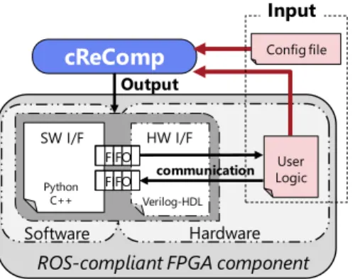
Figure 3 shows the interface generation model of cReComp.
cReComp outputs a component-oriented interface by in- putting two kinds of files. One is an existing user logic, which is a target to be componentized. The other is, in order to allow any customization by developers, a setting descrip- tion file that can define the specification of the interface. The description setting uses Python and scrp (specification for cReComp) which is a special language for cReComp, so that the setting can be done according to the input/output specification of user logic. In addition, the elements that the developer should define to determine the specification of the interface to create the ROS compliant FPGA component, are as follows.
- Bit width of communication channels - Specifying the data port of the user logic - Number of times HW receives data from SW - Number of times HW sends data to SW
- Switching condition between reception and transmis- sion
- Connection between communication path and user logic
By defining the above specifications in the setting de- scription, it is possible to generate a component-oriented interface that can input/output data to/from the user logic without designing the data transfer of componentization. By automating this generation process, a handwriting of data transfer logic can be eliminated, which needs humble verifi- cation and debugging both with HW and SW.
3.2.2 Interface Generated by cReComp
The component-oriented interface generated by cReComp is composed of two kinds of interfaces.
The first one is a circuit description (HW I/F: hard- ware interface) including a communication control state ma- chine. For the component-oriented interface generated by cReComp, xillybus ip[15], which is an IP core for pro- grammable SoC that Xillybus Corporation has released, is
used as a communication path between the FPGA (user logic) and the CPU[16]. The IP core provided by Xilly- bus supports data communication between the FPGA and the CPU, and software’s data input/output to/from the FPGA can be done by file operation to the device file. In the user circuit and the CPU on the FPGA, input and output data can be done by carrying out master control of the FIFO buffer (xillybus ip). The evaluation version of Xillybus ip can use one FIFO buffer with a bit width of 32 bytes and one FIFO buffer with 8 bytes, each with a FIFO buffer for input and output.
By using the IP of the FIFO buffer as the communica- tion path for data input and output respectively, data to be buffered can be read and written at arbitrary timing on both the CPU side and the FPGA side, which means timing devi- ations in data transfer need not be considered. Furthermore, since the control logic related to communication is limited, it is possible to simplify the circuit description of the com- munication path control, and to generate automatically the hardware interface according to the setting description.
The second one is a control software code (SW I/F:
software interface) for inputting/outputting data to/from the user logic. The software interface automatically generates a description for accessing to the communication path pro- vided by xillybus ip. Xillybus in the figure is a class that carries out basic access operations to device files provided by xillybus ip. In the class of user logic, the settings given to cReComp at the time of interface generation and a user logic class that can be operated in upper class by using the Xillybus class, are generated. By adopting such a hierar- chical structure, it is easier for developers to add functional expansions on software interfaces, and to introduce various frameworks.
3.2.3 Realization of Automatic Interface Generation In the ROS-compliant FPGA component, access to the data of the user logic has to be performed by ROS pub- lish/subscribe. Therefore, cReComp needs to shape the data format of ROS message into data that can be handled in FPGA, and to generate automatically an interface with the function of inputting and outputting to the user logic. By defining the signal for data transfer in the user logic with the setting description, cReComp generates automatically an interface which can input/output data directly from the ROS message to the data port of the user logic. Figure 4 shows how input/output signals of user logic are converted into ROS messages. In ROS, messages used for commu- nication between components can be set to any data struc- ture. Consequently, in the example of the user logic shown in Fig. 4, when two 16-bit input signals and a 32-bit output signal are designated as data ports, a variable correspond- ing to the signal is defined in the message. The signal of the specified user logic is assigned to the input/output FIFO buffer in the hardware interface. Besides, for the signal as- signed to the FIFO buffer on the FPGA, the value of each variable in the ROS message is shaped by a shift operation in
Fig. 4 Conversion between logic signal and ROS message
Fig. 5 An example code of configuration by Python
the software interface. Because of this data formatting, it is possible to input and output data to the user logic by reading from and writing to the device file of the FIFO buffer. By us- ing component-oriented interface with the above functions, data input/output to the user logic by ROS publish/subscribe shall be able to be realized, and ROS-compliant FPGA com- ponent can be rapidly introduced into any system.
3.3 Setting Description Method of cReComp
As mentioned in Sect. 3.2.1, the languages that can be used for the setting description are Python and scrp. In this pa- per, Fig. 5 shows an example of setting description using Python. Nearly all the codes shown in Fig. 6 are generated automatically by cReComp’s template generation function.
Therefore, the setting shall be made only for the parts to be changed or added. Setting description by Python is done by using the library provided by cReComp. The setting con- tents related to componentization are stored in the instance of the Component class defined by the library. Describ- ing with Python uses a method, add *(), to add the setting item to the instance of the Component class. For example, add input() and add reg( ) show the addition of user defined signals required for the hardware interface. Xillybus fifo in
Fig. 6 A ROS-compliant FPGA component which drives motor by PWM circuit/signal
the middle of the codes is a class for defining specifications relating to data transfer between the user logic and software.
When the class of Xillybus fifo is declared, each item can be set by giving a parameter to the instance as shown in Fig. 6 or by using a method for each setting item. By using fifo 32.assign (), it is possible to determine the signal to be assigned to the FIFO buffer. Therefore, the signal assigned to the FIFO buffer can be further assigned to the data port of the user logic, which makes it possible to input/output data from the software.
As mentioned above, any component developer can easily make the setting description for the componentiza- tion by calling methods for the class instance of the library provided by cReComp.
4. Evaluation
To evaluate how cReComp affects the productivity of ROS compliant FPGA component development, we conducted experiments with the cooperation of 10 subjects.
4.1 Outline of Evaluation Experiments
The theme of the experiment was to control a DC motor by PWM (Pulse Width Modulation). A circuit description, pwm ctl.v, which can control PWM, was distributed to the subjects as user logic, and they were asked to componen- tize it by cReComp. The experimental environment is sum- marized in Table 1. FPGA board used as the experimental environment was ‘Zedboard’ which was released by Avnet and Digilent equipped with Xilinx Zynq-7020. In addition,
‘Pmod HB 3’ manufactured by Digilent was used as a mo- tor driver for motor control, and the motor was connected to Zedboard via the motor driver.
Figure 6 shows the ROS-compliant FPGA component developed by subjects. The component subscribes to mes- sages that other nodes publish in order to input data to the user logic. The parameters stored in the received message are input to the user logic through the software interface, and the PWM signal is output based on the parameters.
10 subjects joined the experiments. The properties of the 10 subjects are shown in Table 2. The development experiment was proceeded based on the experiment proce- dure guidance site where the author described the experi- ment procedure. Figure 7 shows the experimental proce-
Table 1 Equipment used in the experiments
Table 2 Properties of the 10 Subjects
Fig. 7 Experimental procedure
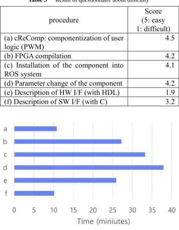
dures. In procedure a, setting description was made to the user logic and componentization was done. In procedures (b) and (c), component introduction and operation confir- mation were carried out, and application development was carried out in procedure (d). Also, in order to study de- velopment productivity of component-oriented interface in both cases of using cReComp and not using cReComp, in procedures (e) and (f), subjects described two types of inter- faces, hardware interface and software interface, which have equivalent functions to the interface descriptions generated in procedure (a). The reference design was shown on the experiment procedure guidance site, and the subject typed each description. As an evaluation of design productivity, time measurement and difficulty evaluation of all procedures were carried out. Evaluation of difficulty was subjective evaluation of 5 stages (5: easy to 1: difficult). We asked the subjects to fill out questionnaire forms, then totaled the results. Table 3 and Fig. 8 show the difficulty evaluation and the required time for each procedure in the experiment. Re- garding the graphs in the figure, the vertical axis on the left is the time taken for each procedure, and the vertical on the right is the difficulty level of 5 stages in each procedure.
The horizontal axis corresponds to the alphabet of the ex- perimental procedure shown in the previous section. The average time taken for all procedures in the experiment was
Table 3 Result of questionnaire about difficulty
Fig. 8 Time to complete each step
2 hours 26 minutes, while the longest required time was 3 hours 18 minutes and the shortest was 1 hour 47 minutes.
4.2 Results and Discussions
The average of the difficulty evaluation value in procedure a was 4.5 (5 at the highest, 3 at the lowest), and the average time required for the procedure was 11 minutes. Among the time required for procedure a, the longest time was 16 minutes and the shortest was 6 minutes. Therefore, regard- less of the development experience in FPGA, it became clear that componentization can be done within a very short time.
Some examples of comments from subjects, who rated the difficulty of procedure a 4 or above are as follows.
• Comment 1: Because of Python, the code is simple and easy to understand
• Comment 2: Defining the necessary signal line and connecting the communication path are all you need
• Comment 3: You only need to consider input/output specifications, then you can easily generate SW that controls HW.
It is possible to use Python for setting descriptions.
That means, as in comment 1, if you have simple knowledge of Python’s grammar, you can easily write setting descrip- tions. Furthermore, since the template generation function of cReComp automatically describes most of the descrip- tion necessary for setting, quick componentization can be
realized. From comments 2 and 3, the component genera- tion model of cReComp has greatly influenced the design productivity. When cReComp is used to convert user logic into ROS-compliant FPGA component, you only need to know the input/output specifications and functions of the user logic. Componentization is easy because you don’t have to design communication paths between hardware and software or interfaces with RTL.
In order to investigate the development productivity of converting the user logic into ROS-compliant FPGA compo- nent without using cReComp, in procedure e and f we asked the subjects to describe the interface having the equivalent function as the interface of procedure a. Two types of files were described, a hardware interface (procedure (a)) and a software interface (procedure (f)). The description contents were shown on the experiment procedure guidance site, and the subjects only needed to type the codes. The average of the difficulty evaluation values of procedure (c)/(f) was 1.9 and 3.2, respectively, which were 1 to 2 points lower than those of procedure a. Also, the average time required was, (c)=26 minutes, (f) =10 minutes, 36 minutes in to- tal. It took more than 20 minutes compared with procedure (a). If ROS-compliant FPGA component is developed with- out using cReComp, there is not only equivalent amount of code writing, but also designing, debugging and verification are inevitable. Now we see clearly, cReComp contributes to shortening development time of ROS-compliant FPGA component, and it makes component development easy.
In procedures (c) and (d), operation confirmation and application development were carried out on Zedboard for the developed ROS-compliant FPGA component. The aver- age difficulty evaluation value of procedure (c) was 4.1, and the average required time was 33 minutes. Subjects who had no experience of developing FPGAs completed each proce- dure within one hour. Regardless of the knowledge about FPGA, we find that the circuit description of the FPGA can be easily handled by using the ROS-compliant FPGA com- ponent generated by cReComp.
Performance issue by this componentizing is also im- portant besides the productivity. Since the HW/SW commu- nication depends on xillybus ip[15], overhead compared to bare HDL is added in terms of latency and area of FPGA re- source. In addition, TCP/IP communication which is done by software on ARM processor is a large overhead. Al- though detailed analysis are done in our previous paper[9], the performance problem still remains as a problem.
5. Related Works
Component-based FPGA design tool discussed in this paper can be categorized into system level design tool. In that context, we can find various research works and commercial products.
“PyGen”[17] is proposed based-on MATLAB/Simu- link. PyGen is written in Python. It is responsible for creating communication between PyGen and MATLAB/
Simulink and mapping the basic building blocks in System
Generator to Python classes. The tool is intended to explore optimum FPGA usage in terms of power consumption at system level. However, usability evaluation is not done yet.
“PyVerilog”[19] is a toolkit of hardware design for Verilog HDL using Python. cReComp uses this toolkit for easy manipulation of Verilog-HDL using Python. There- fore, PyVerilog is rather a general purpose tool compared to cReComp.
COMTA (Connective Object for Middleware To Ac- celerator)[18]is a middleware for robots using FPGA as a hardware accelerator connected to software. The research focuses on how to integrate home-service robot by using high-performance FPGA processing. This middleware is also connectable to ROS (Robot Operating System), how- ever, the development of COMTA itself is not discussed yet.
6. Conclusion
In this paper, we described the realization of cReComp, an automated design tool for improving development produc- tivity of ROS-compliant FPGA component. Also, in order to evaluate the development productivity of robot applications using cReComp, subject experiments were conducted. As a result of experiments, it was confirmed that even subjects without development experience of FPGA finished compo- nentization within 30 minutes. Furthermore, they could fin- ish all the process from componentization to application de- velopment in ROS system for 2 hours 30 minutes on av- erage. The developed cReComp is now open as an open source in Github[20].
Acknowledgments
This research and development work was supported by the MIC/SCOPE #152103014 and JSPS Kakenhi grant (17K00072).
References
[1] R. Siegwart, I.R. Nourbakhsh, and D. Scaramuzza, Introduction to autonomous mobile robots, MIT Press, 2011.
[2] K. Tamura, and K. Naruse, “Unsmooth field sweeping by Bal- istic random walk of multiple robots in unsmooth terrain,” 2014 Joint 7th International Conference on Soft Computing and Intel- ligent Systems (SCIS) and 15th International Symposium on Ad- vanced Intelligent Systems (ISIS), Kitakyushu, pp.585–589, 2014.
doi: 10.1109/SCIS-ISIS.2014.7044837
[3] E.S. Chung, P.A. Milder, J.C. Hoe, and K. Mai, “Single-chip het- erogeneous computing: Does the future include custom logic, FP- GAs, and GPGPUs?,” Proc. 2010 43rd Annual IEEE/ACM Interna- tional Symposium on Microarchitecture, IEEE Computer Society, pp.225–236, 2010.
[4] M. Quigley, K. Conley, B. Gerkey, J. Faust, T. Foote, J. Leibs, and A.Y. Ng, “ROS: an open-source Robot Operating System,” ICRA Workshop on Open Source Software, vol.3, no.3.2, p.5, 2009.
[5] R. Mamat, A. Jawawi, N. Dayang, and S. Deris, “A component- oriented programming for embedded mobile robot software,” Inter- national Journal of Advanced Robotic Systems, pp.371–380, 2007.
[6] J. Boren and S. Cousins, “Exponential growth of ros [ros topics],”
IEEE Robot. Autom. Mag., vol.18, no.1, pp.19–20, 2011.
[7] K. Yamashina, H. Kimura, T. Ohkawa, K. Ootsu, and T.
Yokota, “cReComp: Automated Design Tool for ROS-Compli- ant FPGA Component,” Proc. IEEE 10th International Symposium on Embedded Multicore/Many-core Systems-on-Chip (MCSoC-16), pp.138–145, 2016.
[8] K. Yamashina, T. Matsumoto, T. Ohkawa, K. Ootsu, and T. Yokota,
“Componentizing of FPGA processing for robot, and its evaluation in design productivity,” IEICE Tech. Report, SIG Cloud-Network- Robot (CNR), vol.116, no.461, pp.23–28, 2017.
[9] T. Ohkawa, K. Yamashina, H. Kimura, K. Ootsu, and T. Yokota,
“FPGA Component Technology for Easy Integration of FPGA into Robot Systems,” IEICE Trans. Inf. & Syst. (Special Section on Re- configurable Systems), vol.E101-D, no.2, pp.363–375, Feb. 2018.
DOI: 10.1587/transinf.2017RCP0011
[10] Open Source Robotics Foundation, http://www.osrfoundation.org/ [11] ROS Wiki, http://wiki.ros.org
[12] ROS message, http://wiki.ros.org/msg
[13] L.H. Crockett, R.A. Elliot, M.A. Enderwitz, and R.W. Stewart, The Zynq Book, Strathclyde Academic Media, 2014.
[14] V. Kathail, J. Hwang, W. Sun, Y. Chobe, T. Shui, and J. Carrillo,
“SDSoC: A Higher-level Programming Environment for Zynq SoC and Ultrascale+MPSoC,” Proc. 2016 ACM/SIGDA International Symposium on Field-Programmable Gate Arrays, p.4, ACM, Feb.
2016.
[15] Xillybus, http://xillybus.com/(accessed July 27, 2018)
[16] Q. Zhao, T. Nakamichi, M. Amagasaki, M. Iida, M. Kuga, and T.
Sueyoshi, “hCODE: An open-source platform for FPGA accelera- tors.” Proc. 2016 International Conference on Field-Programmable Technology (FPT), pp.205–208, Dec. 2016.
[17] J. Ou and V.K. Prasanna, “PyGen: a MATLAB/Simulink based tool for synthesizing parameterized and energy efficient designs using FPGAs,” 12th Annual IEEE Symposium on Field-Programmable Custom Computing Machines (FCCM), pp.47–56, 2004.
[18] Y. Ishida, T. Morie, and H. Tamukoh, “A Hardware Acceler- ated Robot Middleware Package for Intelligent Processing on Robots,” 2018 IEEE International Symposium on Circuits and Systems (ISCAS), Florence, Italy, pp.1–5, 2018. doi: 10.1109/ ISCAS.2018.8351722
[19] S. Takamaeda-Yamazaki, “Pyverilog: A python-based hardware de- sign processing toolkit for verilog hdl,” International Symposium on Applied Reconfigurable Computing, vol.9040, pp.451–460, April 2015.
[20] cReComp, https://github.com/kazuyamashi/cReComp
Takeshi Ohkawa received the B.E., M.E.
and Ph.D. degrees in electronics from Tohoku University in 1998, 2000 and 2003 respectively.
He was engaged in research on dynamically re- configurable FPGA device and system at To- hoku University since 2003. He joined National Institute for Advanced Industrial Science and Technology (AIST) in 2004 and started research on distributed embedded systems. He had been working in TOPS Systems Corp on heteroge- neous multicore processor design since 2009.
And he joined Utsunomiya University in 2011 as an assistant professor.
His current research interests are the design technology of an FPGA to re- alize a low power robots and vision systems. He is a member of IEEE, ACM. He is also a member of IEICE, IPSJ, RSJ of Japan.
Kazushi Yamashina received the B.E., M.E. in information systems science from Utsu- nomiya University in 2014 and 2016 respec- tively. He joined Hitachi Ltd. in 2016 and started research and development on FPGA ap- plication of industrial robots.
Takuya Matsumoto received the B.E., M.E.
in information systems science from Utsuno- miya University in 2016 and 2018, respectively.
He joined Mitsubishi Electric Information Net- work Corporation (MIND) in 2018.
Kamemitsu Ootsu received his B.S. and M.S. degrees from the University of Tokyo in 1993 and 1995, respectively, and later he ob- tained his Ph.D. in information science and tech- nology from the University of Tokyo in Japan.
From 1997 to 2009, he was a research associate, and then, in 2009, he became an associate pro- fessor at Utsunomiya University. His research interests are in high-performance computer ar- chitecture, multi-core multi-thread processor ar- chitecture, binary translation and run-time opti- mization. He is a member of IPSJ.
Takashi Yokota received his B.E., M.E., and Ph.D. degrees from Keio University in 1983, 1985 and 1997, respectively. He joined Mit- subishi Electric Corp. in 1985, and was engaged in several research projects in special-purpose, massively parallel and industrial computers. He was engaged in research and development of a massively parallel computer RWC–1 at Real World Computing Partnership as a senior re- searcher from 1993 to 1997. From 2001 to 2009, he was an associate professor at Utsunomiya University. Since 2009, he has been a professor at Utsunomiya Univer- sity. His research interests include computer architecture, parallel process- ing, network architecture and de-sign automation. He is a member of IPSJ, IEICE and the IEEE Computer Society.