320
IEICE TRANS. ELECTRON., VOL.E96–C, NO.3 MARCH 2013
INVITED PAPER
Special Section on SQUID & its ApplicationsNovel Superconducting Quantum Interference Device Bootstrap Circuit and Its Application in Biomagnetism
Xiangyan KONG†,††a),Member, Yi ZHANG†††,††b), Xiaoming XIE†,††,andMianheng JIANG†,††,Nonmembers
SUMMARY The voltage biased SQUID Bootstrap Circuit (SBC) was recently demonstrated for direct readout of SQUID signals. The SBC com- bines current- and voltage-feedbacks in one circuit to suppress the pream- plifier noise. It offers not only a good noise performance, but also wide tolerance of SQUID parameters. Using SBC gradiometer, the bio-magnetic signals were successfully measured. In this paper, we overview the concept of SBC and its applications.
key words: SQUID bootstrap circuit (SBC), SQUID readout electronics, SQUID noise, biomagnetic measurement
1. Introduction
LowTc dc superconducting quantum interference devices (SQUIDs) are widely used in biomagnetic measurements due to their ultra high sensitivity. For SQUID readout elec- tronics, it is always a tough challenge to keep the preampli- fier noise contribution below the SQUID intrinsic noise and to simplify the readout electronics.
Usually, the dc SQUID can be operated in two modes — the current bias mode and the voltage bias mode.
In principle, no difference exists between the above two modes for SQUID intrinsic noise [1].
In order to reduce the preamplifier noise, there are dif- ferent readout approaches. The standard is the flux modula- tion (FM) scheme [2]. In FM, a transformer is used to trans- late the low impedance of the SQUID to the high impedance of the preamplifier.
In biomagnetic SQUID multichannel systems, two types of direct readout techniques without FM were devel- oped in the early 1990s to simplify the readout electron- ics. One is additional positive feedback (APF), which is operated in current bias mode [3]. It enhances the flux-to- voltage transfer coefficient to suppress the flux noise con- tribution of the preamplifier by setting a working point on the steep slope of a strongly asymmetricV-Φcharacteristic.
The other one, called noise cancellation (NC), is proposed Manuscript received July 18, 2012.
Manuscript revised November 6, 2012.
†The authors are with State Key Laboratory of Functional Ma- terials for Informatics, Shanghai Institute of Microsystem and In- formation Technology (SIMIT), Chinese Academy of Sciences (CAS), Shanghai 200050, China.
††The authors are with Joint Research Laboratory on Su- perconductivity and Bioelectronics, Collaboration between CAS- Shanghai and FZJ, Shanghai 200050, China.
†††The author is with Peter Gr¨unberg Institute (PGI-8), Forschungszentrum J¨ulich (FZJ), D-52425 J¨ulich, Germany.
a) E-mail: [email protected] b) E-mail: [email protected]
DOI: 10.1587/transele.E96.C.320
by Sepp¨a et al. and is operated in voltage bias mode [4]. The NC increases the dynamic resistance of NC circuit, thus re- ducing the preamplifier noise.
In this paper, we overview one alternative direct read- out scheme called SQUID bootstrap circuit (SBC) [5], which was proposed by the scientists in Chinese Academy of Sciences and J¨ulich Research Center, Germany. In the past four years, SBC was introduced [5]–[7], the parame- ter tolerances were discussed [8], [9], a gradiometer mod- ule with pickup antenna and integrated voltage feedback cir- cuit was developed [10], and the biomagnetic measurements were performed [11].
2. SQUID Bootstrap Circuit (SBC)
In voltage bias mode, the dc SQUID can be considered as a flux-to-voltage (∂V/∂Φ) converter and the dynamic resis- tance of the SQUIDRd, which are connected in series. If a constant bias voltageVbis applied across the dc SQUID, an external magnetic fluxφe causes a current change through the SQUID determined by (∂i/∂Φ)=(∂V/∂Φ)/Rd. The cur- rentiis periodically modulated by the external magnetic flux φe. Periodicity of the I-Φcharacteristic is the flux quantum Φ0.
The noise from the preamplifier contains two compo- nents — the voltage noiseVnand the current noiseIn∗. Usu- ally,Vndominates the noise contribution of the preamplifier in the direct readout schemes. In the voltage bias mode, the equivalent flux noise of a preamplifier is expressed as δΦpreamp=Vn/[Rd(∂i/∂Φ)].
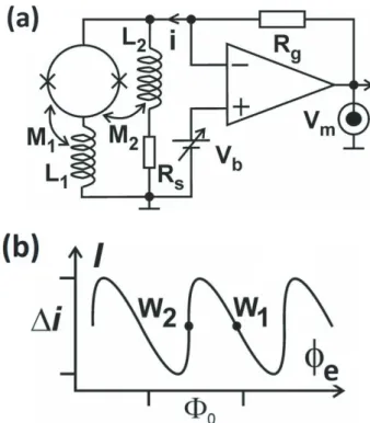
The voltage biased SQUID bootstrap circuit (SBC) consists of two parallel branches B1 and B2 shown in Fig. 1(a): B1 comprises the dc SQUID and the feedback coil of inductanceL1 connected in series. L1is inductively coupled to the SQUID loop with a mutual inductance M1. Branch B1is shunted by B2consisting of a shunt resistorRs
and a coil of inductanceL2, which is coupled to the SQUID with a mutual inductanceM2. The room temperature read- out circuit is also shown in Fig. 1(a) while the flux-locked loop (FLL) is omitted. The bias voltage sourceVb is con- nected to the non-inverting input terminal of the preampli- fier. The preamplifier acts as a current-to-voltage converter, and its conversion gain depends onRg. The current versus flux characteristic of the SBC can be monitored from the preamplifier outputVm.
B1of SBC is a current feedback and changes the flux- to-current coefficient, while B2is a voltage feedback and in- Copyright c2013 The Institute of Electronics, Information and Communication Engineers
Fig. 1 (a) SBC circuit with the preamplifier. SBC consists of two branches, B1and B2, which act as current feedback and voltage feedback, respectively. (b) the asymmetricI-Φcharacteristics of the SBC. The work- ing point can be set on either the gradual slope W1or the steep slope W2.
creases the dynamic resistanceRd to suppress the preampli- fier noise. The functions of B1without B2can be described as:
(∂i/∂Φ)B1=(∂i/∂Φ)/[1−M1(∂i/∂Φ)] (1) R(Bd1)=Rd[1−M1(∂i/∂Φ)] (2) According to the above two equations, the product of (∂i/∂Φ)B1 and R(Bd1) keeps constant. Therefore, B1 alone does not contribute to the reduction ofδΦpreamp. At the crit- ical condition ofM1•(∂i/∂Φ)=1,R(Bd 1) → 0 at the work- ing point W2 orR(Bd 1) ≈ 2Rd at the working point W1 (see Fig. 1(b)) [5].
Now we analyze both branches together and take into account the voltage noiseVnfrom the preamplifier. The bias voltage can be expressed asVb +Vn. Here, the dc volt- ageVbhas already been adjusted to the optimal value. The bias voltage (Vb+Vn) and the voltage change across SQUID caused byφeonly act as potentials. The corresponding volt- ages are generated by the currenti+in, which always flows from the output of the preamplifierVmviaRg to SBC (see Fig. 1).
The equivalent circuit of the noise current caused by Vnis shown in Fig. 2. The following noise analysis applies at low frequencies whenωnL1,2R(B1)d ,Rs. Here,ωnis the noise frequency. In the circuit, branch B1is expressed as the dynamic resistanceR(Bd1) and a potential (battery)Vsn con- necting in series.Vsnis generated by the noise fluxin2M2in the SQUID loop via∂V/∂Φof the SQUID, where the noise currentin2=Vn/Rs. Branch B2is denoted as the shunt resis-
Fig. 2 The noise equivalent circuit of SBC. The noise current flows from the output of the preamplifier into the two parallel branches B1and B2.The noise voltageVnis across each branch. Vsnis the noise voltage generated by the noise fluxin2M2across the SQUID.
torRs, if the impedanceωnL2 can be neglected. The noise voltageVnis across the two branches (see Fig. 2). AsVnand Vsnhave the same polarity, in1 decreases. Under the “criti- cal condition”Vn =Vsn of B2,in1disappears,in =in2and the dynamic resistance of total SBCR(SBC)d =Rs. WhenRs
is larger thanRdof the bare SQUID, the noise of preampli- fier can be effectively suppressed [5]. Comparison of noise measurements with SBC and FM scheme was performed. In such measurements, several liquid-helium-cooled SQUID magnetometers with different layouts and SQUID loop in- ductances were employed. Measured noise of SBC was comparable to or even lower than that of FM scheme [7].
Two numerical simulations — one based on SBC equivalent circuit and the other one on the basic Joseph- son RCSJ model and network equations — were performed [6], [12]. Both simulations showed that the SBC provides a good flexibility in both parameter choice and wide margins for their adjustment.
The difference between SBC and NC is the introduc- tion of a current feedback into the SBC circuit. The current feedback (branch B1) significantly extends the linear range at the working point, thus increasing system stability and slew rate [13]. Furthermore, the current feedback can im- prove parameter tolerances [8] to enhance the sample fabri- cation yield.
An ideal voltage source with zero intrinsic resistance Rinis very difficult to realize. To study the influence of volt- age source resistance Rin on the SBC parameters (i.e., the flux-to-current transfer coefficient (∂I/∂Φ)SBC and the dy- namic resistanceR(SBC)d as well as the noise performance), an additional variable room-temperature resistorRad between the liquid-helium-cooled SQUID and the preamplifier was
322
IEICE TRANS. ELECTRON., VOL.E96–C, NO.3 MARCH 2013
introduced. The measured SQUID noise remains practically unchanged forRad of less than 50Ω. Low-temperature ca- bles with low thermal conductivity but high resistivity can be chosen to reduce the total heat loss in the SBC scheme without compromising the sensitivity, which is of great im- portance in multi-channel applications [14].
3. SBC Gradiometer Module
In biomagnetic measurements, planar or axial gradiometers are generally used to suppress external interference, thus en- hancing the measurement signal-to-noise ratio (SNR). We developed a planar dual-loop gradient SQUID with an input coil connecting a niobium wire-wound antenna to construct an SBC axial gradiometer [10].
3.1 SQUID Chip Design
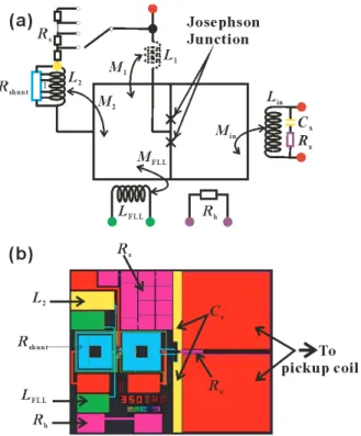
Figure 3(a) is an equivalent circuit of a SQUID chip, which includes a washer SQUID, two SBC coilsL1andL2, a flux feedback coilLFLLfor the flux locked loop, an input coilLin
connecting an axial wire-wound first-order gradient pickup antenna, and a shunt resistorRsconnectingL2in series, and a resistorRhfor heating the SQUID.
Here, a dual-loop washer-SQUID is employed to sup- press external magnetic disturbances and to provide space for setting different coils. However, due to shortage of space, the SBC current feedback coilL1is absent in the first setup. Therefore, the SBC readout scheme in this design is simplified to a NC circuit. The coilsL2andLFLLare induc- tively coupled to the left loop of the SQUID via the mutual inductancesM2andMFLL, while the input coilLincouples to the right loop of SQUID viaMin. The SQUID is shunted by a voltage feedback circuit consisting ofL2andRs. Several optional planar resistorsRsare placed on the chip. In this de- sign, a resistor-capacitor serial branchRx−Cxwas inserted to shunt the input coilLinwith a low pass filter in order to reduce the high frequency disturbance from the pickup an- tenna. Besides, the planarL2 coil is covered by a resistor stripRshunt to damp the resonance phenomena originating from the parasitic capacitance between the SQUID washer and the integrated coil.
The practical SQUID-chip layout is shown in Fig. 3(b).
The junction size is 3μm×3μm and its shunted resistance is 20Ω. One SQUID hole size is 280μm×280μm. The SQUID inductance is estimated to be 350 pH. The turns of coils L2, LFLL and Lin are 26, 3 and 27, respectively.
The measured mutual inductances M2, MFLL and Min are 2.35 nH, 0.13 nH and 2.4 nH, respectively. The designed re- sistanceRxis 610Ω(4.2 K) and capacitanceCx10 pH. The heating resistanceRh is designed as 160Ω(4.2 K) and the SBC shuntRs80∼240Ω(4.2 K). One can choose a suitable resistor Rs from several discrete thin-film resistors fabri- cated on the chip in order to obtain the optimum dynamic re- sistance of SBC circuit. With two large pads of size 2.2 mm
×1.9 mm at the terminals of the input coil, it is convenient to realize the superconducting connection between the input
Fig. 3 (a) The equivalent circuit of SQUID chip (the current feedback coilL1 which is needed for SBC readout but is missing in our experi- ment is sketched by a dashed line), (b) the designed layout on a chip of 5 mm×4 mm.
coil and the antenna.
3.2 SBC Gradiometer Module
The gradiometer module with direct readout circuit consists of an Nb-SQUID chip, an axial Nb wire-wound first-order gradient pickup antenna, a polymer supporter, and an Nb shielding tube. The schematic diagram of the SBC gra- diometer is shown in Fig. 4(a). The planar SQUID chip is encapsulated after choosingRs.
The pickup antenna is a first-order gradient coil with a diameter of 10 mm. The inductance of the pickup coil is estimated to be 400 nH, which is somewhat smaller than that of the input coil of about 500 nH. The superconduct- ing connection between the input coil and the pickup coil is realized by soldering lead-indium (PbIn) alloy. Finally, the encapsulated SQUID chip and the antenna are mounted on a polymer supporter. A thin niobium shielding tube is used to eliminate the environmental signal detected by the SQUID itself. Figure 4(b) shows the gradiometer module.
3.3 Calibration of SBC Gradiometer
The sensitivity of the gradiometer module was measured in- side a magnetically shielded room (MSR). The gradiome- ter module was mounted on the bottom of a non-magnetic liquid helium cryostat. A calibrating reference coil with a diameter of 20 cm and 5 turns was placed under the De- war. The distance between the reference coil and the bot-
Fig. 4 Structure of the SBC gradiometer module. (a) Schematic diagram of the SBC gradiometer, (b) photograph of the fabricated gradiometer. The baseline of the gradient antenna is 50 mm. (c) the noise spectrum of SBC gradiometer measured in MSR.
tom loop of the axial gradient antenna was 63 mm. Using Biot-Savart’s law, the gradient field-to-flux transfer coeffi- cient could be obtained by calculation.
The field sensitivity of this module was measured to be about 1 fT/(cm·√
Hz) at 100 Hz as shown in Fig. 4(c).
This corresponds to a magnetometer noise of 5 fT/√ Hz for a current loop with very small diameter. A noise contri- bution from mechanical vibrations clearly appeared in low frequency range (<50 Hz) for the simple setup of the mea- surement system.
4. Biomagnetic Measurements Using SBC Gradiome- ter Module
Using above SBC gradiometer module, the biomagnetic measurements were performed in a magnetically shielded room (2.5 m×2.5 m×2.4 m) with moderate shielding fac- tors (60 dB@1 Hz, 47 [email protected]). The bottom thickness of the nonmagnetic fiber glass liquid helium cryostat is about 16 mm. The outputs of FLL are recorded by a 24-bit acqui-
Fig. 5 Real-time (a) and averaged (b) MCG signals of a 28-year old adult subject.
Fig. 6 Recorded fMCG signal with 30 weeks gestation: (a) Multi-cycle signal after baseline removal; (b) Averaged signal.
sition system.
Firstly, magnetocardiographic (MCG) signals of a 28- year-old adult subject were recorded with a sample rate of 2560 Hz. Figure 5(a) is the 30 s real-time MCG signals with 150 Hz low-pass filter. Here, the signal-to-noise ratio (SNR) is more than 50 according to the peak-to-peak value of MCG signal and noise and the R-peak of the MCG signal is ap- proximately 40 pT. The averaged MCG signal is shown in Fig. 5(b) with a period of 0.73 s and its SNR is obviously improved (larger than 100).
The second experiment was to measure a fetus’ heart of 30 weeks gestation.
Before the measurement, the position of the fetus’ heart is firstly found with a fetus-voicemeter. The liquid helium cryostat should lean with a certain angle to reach the mini- mum distance between maternal abdomen and the measur- ing sensor. Figure 6(a) shows the recorded multi-cycle fetal MCG (fMCG) signal after removing the baseline drift by wavelet transformation. The amplitude is around 1 pT and the SNR of the real time fMCG is about 5. The noise mainly comes from the breath of the mother or the movement of the
324
IEICE TRANS. ELECTRON., VOL.E96–C, NO.3 MARCH 2013
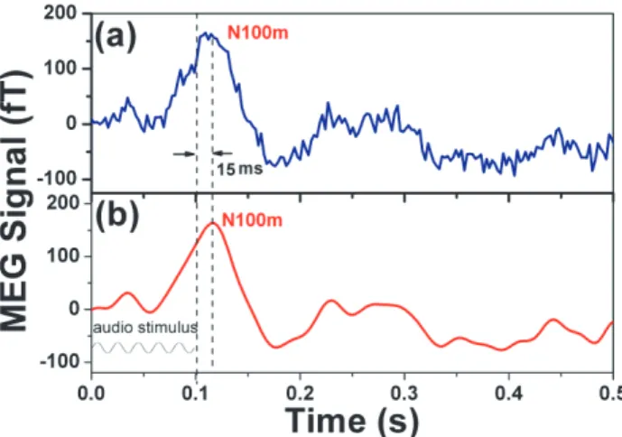
Fig. 7 Auditory evoked magnetic field with 100 times average:
(a) Unprocessed; (b) After 35 Hz low-pass filter.
fetus. Figure 6(b) is the averaged signal and the amplitude of R peak is about 0.8 pT and the cardiac cycle of the fetus is 0.43 s.
In the third experiment, magnetoencephalographic (MEG) signals from auditory evoked magnetic field were measured. The stimulus at 1000 Hz frequency were gener- ated for duration of 100 ms and presented monaurally using Etymotic ER-30 earphones. The audio signals were trans- mitted to the right ear of the subject with a repetition rate of 1.1 s. MEG signals were measured over the left tempo- ral lobe. The sampling rate is 375 Hz. Figure 7(a) shows the trace of the auditory-evoked response with 100 averages and (b) is that with a 35 Hz low pass filter.
The trace exhibits a prominent peak (N100 m), which should appear at the latency of about 100 ms after the onset of the stimulus, and represents the response that occurs in the primary auditory cortex. However, the N100 m peak in Fig. 7 appeared at about 115 ms (not the predicted 100 ms) because of approximate 15 ms delay of the audio transmis- sion through a soft plastic pipe of 5 m length.
In this section, we mainly overviewed the design, fab- rication and evaluation of the SBC first-order gradiome- ter. Its sensitivity reached 1 fT/(cm·√
Hz) at 100 Hz inside the MSR. As a demonstration, human MCG and auditory- evoked MEG signals were successfully recorded with this module. We reported the fMCG signal in MSR for the first time in China using low Tcdc SQUID.
5. Conclusion and Outlook
In this paper, we overview our works in the past four years:
a) the operating principle of the novel SQUID bootstrap cir- cuit (SBC) is described; b) numerical simulations based on SBC equivalent circuit, or on the basic Josephson RCSJ model and network equations are performed; c) measured noise of SBC was comparable to or even lower than that of FM scheme; d) SBC parameters such as M1, M2, and Rs are optimized and their functions are discussed in de- tail; e) A SBC axial gradiometer module with wire-wound
pickup antenna is constructed and its sensitivity reached about 1 fT/(cm·√
Hz) at 100 Hz. Using this SBC gradiome- ter, MCG, auditory evoked MEG signals and fMCG sig- nals were successfully obtained in a moderate MSR built in SIMIT Jiading campus.
The integrated SBC concept with simple readout elec- tronics is ideal not only for multi-channel applications, but also for readout of radiation detector arrays, etc.
Acknowledgments
This work was supported by several funding sources: the bilateral cooperation on education and research, the In- ternational Bureau of the German BMBF at DLR, Grant CHW09/009; funding from Chinese Academy of Sciences for international cooperation (Contract: GJHZ1104), fund- ing from Knowledge Innovation Program of the Chinese Academy of Sciences (Grant No: KGCX2-YW-906 and KGCX2-EW-105) and One Hundred Person Project of the Chinese Academy of Science.
References
[1] D. Drung and M. M¨uck, “SQUID electronics,” The SQUID Hand- book vol.I, ed. J. Clarke and A.I. Braginski (Weinheim: Wiley–
VCH) pp.127–70, 2004.
[2] R.L. Forgacs and A. Warnick, “Digital-analog magnetometer uti- lizing superconducting sensor,” Rev. Sci. Instrum., vol.38, no.2, pp.214–220, Feb. 1967.
[3] R. Cantor, D. Drung, M. Peters, H.J. Scheer, and H. Koch, “Inte- grated DC SQUID magnetometer with simplified read-out,” Super- cond. Sci. Technol., vol.3, no.2, pp.108–112, Feb. 1990.
[4] M. Kiviranta and H. Sepp¨a, “DC-SQUID electronics based on the noise cancellation scheme,” IEEE Trans. Appl. Supercond., vol.5, no.2, pp.2146–2148, June 1995.
[5] X. Xie, Y. Zhang, H. Wang, Y. Wang, M. M¨uck, H. Dong, H.-J.
Krause, A.I. Braginski, A. Offenhausser, and M. Jiang, “A voltage biased superconducting quantum interference device bootstrap cir- cuit,” Supercond. Sci. Technol., vol.23, no.6, 065016, June 2010.
[6] Y. Wang, X. Xie, H. Dong, G. Zhang, H. Wang, Y. Zhang, M. M¨uck, H.-J. Krause, A.I. Braginski, A. Offenh¨ausser, and M. Jiang, “Volt- age biased SQUID bootstrap circuit: Circuit model and numerical simulation,” IEEE Trans. Appl. Supercond., vol.21, no.3, pp.354–
357, June 2011.
[7] Y. Zhang, G. Zhang, H. Wang, Y. Wang, H. Dong, X. Xie, M. M¨uck, H.-J. Krause, A.I. Braginski, A. Offenh¨ausser, and M. Jiang, “Com- parison of noise performance of the dc SQUID bootstrap circuit with that of the standard flux modulation dc SQUID readout scheme,”
IEEE Trans. Appl. Supercond., vol.21, no.3, pp.501–504, June 2011.
[8] G. Zhang, Y. Zhang, H. Dong, H.-J. Krause, X. Xie, A.I. Braginski, A. Offenh¨ausser, and M. Jiang, “Parameter tolerance of the SQUID bootstrap circuit,” Supercond. Sci. Technol., vol.25, no.1, 015006, Jan. 2012.
[9] G. Zhang, Y. Zhang, H. Dong, H.-J. Krause, X. Xie, A.I. Braginski, A. Offenh¨ausser, and M. Jiang, “SQUID bootstrap circuit with a large parameter tolerance,” Chin. Phy. Lett., vol.30, no.1, 018501, 2013.
[10] G. Zhang, Y. Zhang, S. Zhang, H.-J. Krause, Y. Wang, C. Liu, J.
Zeng, Y. Qiu, X. Kong, H. Dong, X. Xie, A. Offenh¨ausser, and M.
Jiang, “A SQUID gradiometer module with wire-wound pickup an- tenna and integrated voltage feedback circuit,” Physica C, vol.480, pp.10–13, May 2012.
[11] S. Zhang, G. Zhang, Y. Wang, J. Zeng, Y. Qiu, M. Liu, X. Kong, X.
Xie, and Y. Zhang, “Biomagnetic signal measurements with novel low-Tc DC SQUID bootstrap circuit (SBC),” accepted by Chin. Sci.
Bull., 2013.
[12] H. Wang, Y. Wang, H. Dong, Y. Zhang, X. Xie, H.-J. Krause, and A. Offenh¨ausser, “Noise behavior of SQUID bootstrap circuit stud- ied by numerical simulation,” Physics Procedia, vol.36, pp.127–132, July 2012.
[13] G. Zhang, Y. Zhang, H. Dong, H.-J. Krause, X. Xie, A.I Braginski, A. Offenh¨ausser, and M. Jiang, “An approach to optimization of the superconducting quantum interference device bootstrap circuit,” Su- percond. Sci. Technol., vol.24, no.6, 065023, June 2011.
[14] H. Dong, G. Zhang, Y. Wang, Y. Zhang, X. Xie, H.-J. Krause, A.I.
Braginski, and A. Offenh¨ausser, “Effect of voltage source internal resistance on the SQUID bootstrap circuit,” Supercond. Sci. Tech- nol., vol.25, no.1, 015012, Jan. 2012.
Xiangyan Kong received the Ph.D. in Insti- tute of Physics, Chinese Academy of Sciences in 2005. During 2005–2010, she stayed in Osaka University as a postdoctor. She is now with Shanghai Institute of Microsystem and Informa- tion Technology, Chinese Academy of Sciences.
Yi Zhang received his Bachelor degree in 1982 at the Shanghai Jiao TongUniversity, Mas- ter Degree in 1987 and Ph.D. degree in 1990 at the Justus-Liebig University Gießen, Germany.
He has great achievements in to the fabrica- tion of high Tc SQUIDs and low Tc SQUIDs, SQUID readout, SQUID application in biomag- netism, low-field NMR/MRI and geophysics.
Now he is with Peter Gr¨unberg Institute (PGI- 8), Forschungszentrum J¨ulich.
Xiaoming Xie received bachelor degree of science in 1985 at Wuhan University, Ph.D in 1990, in Shanghai Institute of Microsystem
& Information Technology (SIMIT), Chinese Academy of Sciences (CAS). During 1993–
1995, he was a post-doctor in Ecole Sup´erieure de Physique et de Chimie Industrielles de La Ville de Paris (ESPCI), France. Now he is with Shanghai Institute of Microsystem and Informa- tion Technology, Chinese Academy of Sciences.
Mianheng Jiang received his Ph.D. in Drexel University in 1991. He was the president of Shanghai Institute of Microsystem and Infor- mation Technology (SIMIT), Chinese Academy of Sciences (CAS) from 1997 to 2002. Now he is professor and group leader of superconductiv- ity in SIMIT.