Qubit Fidelity
Author J.P.G. van Dijk, E. Kawakami, R.N. Schouten, M. Veldhorst, L.M.K. Vandersypen, M. Babaie, E. Charbon, F. Sebastiano
journal or
publication title
Physical Review Applied
volume 12
number 4
page range 044054
year 2019‑10‑24
Publisher American Physical Society Author's flag publisher
URL http://id.nii.ac.jp/1394/00001226/
doi: info:doi/10.1103/PhysRevApplied.12.044054
Impact of Classical Control Electronics on Qubit Fidelity
J.P.G. van Dijk,1,2,*E. Kawakami,3R.N. Schouten,1,2M. Veldhorst,1,2L.M.K. Vandersypen,1,2,4 M. Babaie,1E. Charbon,1,2,4,5and F. Sebastiano1
1QuTech, Delft University of Technology, P.O. Box 5046, 2600 GA Delft, Netherlands
2Kavli Institute of Nanoscience, P.O. Box 5046, 2600 GA Delft, Netherlands
3Okinawa Institute of Science and Technology, Okinawa 904-0412, Japan
4Intel Corporation, 2501 NW 229th Ave, Hillsboro Oregon 97124, USA
5École Polytechnique Fédérale de Lausanne, Case postale 526, CH-2002 Neuchâtel, Switzerland
(Received 17 March 2018; revised manuscript received 30 May 2019; published 24 October 2019) Quantum processors rely on classical electronic controllers to manipulate and read out the state of quantum bits (qubits). As the performance of the quantum processor improves, nonidealities in the classi- cal controller can become the performance bottleneck for the whole quantum computer. To prevent such limitation, this paper presents a systematic study of the impact of the classical electrical signals on the qubit fidelity. All operations, i.e., single-qubit rotations, two-qubit gates, and readout, are considered, in the presence of errors in the control electronics, such as static, dynamic, systematic, and random errors.
Although the presented study could be extended to any qubit technology, it currently focuses on single- electron spin qubits, because of several advantages, such as purely electrical control and long coherence times, and for their potential for large-scale integration. As a result of this study, detailed electrical speci- fications for the classical control electronics for a given qubit fidelity can be derived. We also discuss how qubit fidelity is affected by the limited performance of the general-purpose room-temperature equipment typically employed to control the few qubits available today. Ultimately, we show that tailor-made elec- tronic controllers can achieve significantly lower power, cost, and size, as required to support the scaling up of quantum computers.
DOI:10.1103/PhysRevApplied.12.044054
I. INTRODUCTION
Quantum computers have the potential to solve problems that are intractable even for the most powerful supercomputers [1]. These problems include the factor- ization of prime numbers using Shor’s algorithm [2], the efficient search in large data sets using Grover’s algorithm [3], and the simulation of quantum systems as initially proposed by Feynman [4]. A quantum computer oper- ates by processing the information stored in quantum bits (qubits), which are organized in a quantum processor.
Performing operations on the qubits requires a classical electronic controller for manipulating the qubits and read- ing out their quantum state [5]. In order not to degrade qubit performance, the classical controller must provide high-accuracy low-noise control signals and the readout
Published by the American Physical Society under the terms of theCreative Commons Attribution 4.0 Internationallicense.
Further distribution of this work must maintain attribution to the author(s) and the published article’s title, journal citation, and DOI.
must be very sensitive and quiet to detect the weak signals from the quantum processor without altering the qubit states.
Since state-of-the-art quantum processors comprise only a few qubits (<20 qubits [6–8]), the classical controller is currently typically implemented by general-purpose instruments operating at room temperature or tailor-made room-temperature controllers [9,10]. For a recent review of state-of-the-art electronic interface for quantum proces- sors, see Ref. [11]. The use of these high-performance instruments results in the fidelity of the quantum oper- ations being limited by the quantum processor [12].
However, as the performance of the quantum processor improves, the classical controller can become performance limiting. Consequently, it is crucial to understand how the controller impacts the performance of the whole quantum computer in order to properly codesign the controller and the quantum processor and to identify potential perfor- mance bottlenecks.
Moreover, the simplest nontrivial algorithms, such as quantum-chemistry problems, require more than 100 logi- cal qubits [13]. This translates into the need for thousands or millions of physical qubits, if the redundancy added by
quantum-error correction schemes, such as surface codes [14], is taken into account. For such large-scale quan- tum processors, implementation of the classical controller with general-purpose instruments would be impractical and would offer limited scalability due to its size and cost. A more practical and power-efficient approach would be to use tailor-made electronics that can be optimized for this specific application in terms of power consump- tion, form factor, and cost [5,11,15–23]. However, defining the specifications to design such electronics requires a comprehensive analysis of the impact of the electronics performance on the quantum computer.
Furthermore, solid-state qubits need to be cooled to deep cryogenic temperatures. When operating the control electronics at cryogenic temperatures to relax the wiring requirements between the cryogenic quantum processor and its controller, as proposed in Refs. [5,15–20], the need for accurate specifications is even more severe. The power dissipation of such a cryogenic controller is lim- ited by the cooling power of the cryogenic refrigerator.
For existing fridges, this is only about 1 W at 4 K and
<1 mW below 100 mK [24]. Although this could improve in the future by, e.g., adopting custom-made refrigera- tors [25], the power consumption of the controller is also expected to increase to serve an increasing number of qubits. To meet these cooling constraints, the power dis- sipated by the electronics must be minimized by optimally allocating the available power across the various compo- nents of the classical controller. However, carrying out such optimization also demands a clear understanding of the impact of each component on the quantum-computer performance.
Analysis of the impact of the controller on the quantum computer’s performance has been undertaken previously, but only for specific aspects of the control signals, i.e., the effect of microwave phase noise [26,27], or for theoreti- cally treating the effects of noise on qubit operations in a filter function framework [28,29], and control sweet spots [30–32] and noise effects in general [33–35]. The work presented here aims to provide a comprehensive analysis of the effect of nonideal circuit blocks in the classical con- troller on the qubit fidelity for all possible operations, i.e., single-qubit gates, two-qubit gates, and readout. Initializa- tion is assumed to be performed by relaxation or by readout and will not be separately discussed. This includes the effect of signal inaccuracies in the frequency, voltage, and time domain, and covers static, dynamic, systematic, and random errors. Only with a full set of specifications can potential bottlenecks be identified and tailor-made elec- tronics designed. Besides providing a general method for deriving the electronics specifications, the specifications resulting from a case study targeting a 99.9% average gate fidelity are mapped onto existing room-temperature inte- grated circuits (IC) to assess the feasibility of a practical controller.
Although the proposed approach can be easily extended to any quantum technology, such as NMR [36–38], ion traps [8,39], superconducting qubits [7,40,41], or nitrogen- vacancy (N-V) centers in diamond [42], we focus on the specific case of single-electron spin qubits. This qubit tech- nology offers promising prospects for large-scale quantum computing, due to the long coherence times [12,43], the fully electrical control [44,45], and the potential integra- tion of the quantum processor with a classical controller on a single chip fabricated using standard microelectronic technologies [46]. In addition, the results obtained for the single-qubit gates can be generalized to any qubit system where single-qubit rotations are performed by applying a signal with a frequency matching the energy-level spacing between the|0and|1states, e.g., for NMR [36–38], ion traps [8,39], N-V centers in diamond [42], and supercon- ducting qubits [7,40,41]. Similarly, the results obtained for the two-qubit gates can be generalized to any qubit system that exploits the exchange gate.
The paper is organized as follows: Sec. II describes the generalized spin-qubit quantum computer analyzed in this paper; Sec.IIIintroduces the method for deriving the fidelity for the various operations; and in Secs.IV,V, and VI the electrical specifications required for single-qubit operations, two-qubit operations, and qubit readout are derived, respectively. A discussion regarding the feasibil- ity of these specifications follows in Sec.VII. Conclusions are drawn in Sec.VIII.
II. A SYSTEM-LEVEL VIEW OF A QUANTUM COMPUTER
A. The quantum processor
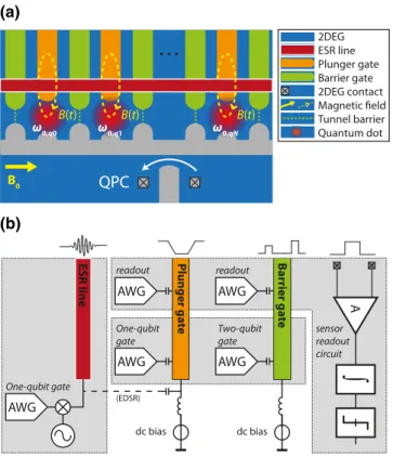
A single-electron spin qubit encodes the quantum state in the spin state of a single electron. A generic model of a quantum processor based on single-electron spin qubits is shown in Fig.1(a), which captures all of the properties relevant for the interaction with the controller. Moreover, the figure illustrates a linear array of quantum dots but this can be extended to more complex geometries such as a 2D grid of quantum dots, as shown in Refs. [46–48].
Quantum dots are formed using a set of gate elec- trodes that locally deplete a two-dimensional electron gas (2DEG) on a semiconductor chip (e.g., a GaAs/(Al,Ga)As heterojunction, a Si/SiGe heterojunction, or a Si–metal- oxide semiconductor (MOS) structure [49,50]). Due to the small size of the quantum dot, the charge states become discrete with an energy-level spacing related to the dot charging energy, thereby setting the required increase of the dot potential to add an electron to the dot. The dot potential, and thereby the number of electrons in the dot, is controlled by the plunger gate that capacitively couples to the quantum dot. Without loss of generality for the analy- sis of the electrical control signals, the following analysis assumes the availability of additional tunnel-barrier gates
B(t) B(t) B(t)
2DEG ESR line Plunger gate Barrier gate 2DEG contact Tunnel barrier Quantum dot
B0 QPC
ω0,q0 ω0,q1 ω0,qN
AWG
One-qubit gate
AWG AWG
AWG AWG
Two-qubit gate readout readout
dc bias
∫
sensor readout circuit
ESR line Barrier gate
Plunger gate
dc bias
A
(EDSR) One-qubit gate
(a)
(b)
FIG. 1. (a) A generic model of a spin-qubit quantum proces- sor comprising qubits encoded in the spin of electrons trapped in quantum dots and a charge sensor (e.g., a quantum point con- tact, QPC). The blue background indicates the two-dimensional electron gas (2DEG) where quantum dots, shown in red, are formed locally. Individual control over the dot potential and the tunnel barriers is assumed, using plunger gates (orange) and barrier gates (green), respectively. Furthermore, each qubit can have a unique Larmor frequency (ω0,qi). (b) The classical control electronics required for each line type (electron-spin-resonance (ESR) line, plunger gate, and barrier gate) of the quantum proces- sor. The electronic components in the figure are placeholders for the respective functionalities and are grouped by operation, i.e., single-qubit operation, two-qubit operation, and readout. Thus, they do not necessarily correspond to a physical implementa- tion. Arbitrary-waveform generators (AWG) are shown for the envelope and pulse generation.
that form tunnel barriers between neighboring dots by con- trolling the width of the depletion layer, thus allowing tunneling of electrons from and to the quantum dot in a tunable way. Early integration schemes involved nonover- lapping gates [as shown in Fig.1(a)] [44,51,52], while, in order to create better tunability and control, architectures now often include overlapping gates [45,53–55].
An external static magnetic field B0induces an energy difference between electrons with spin up and spin down, with Zeeman energy Ez. Because of the static magnetic field, the electron rotates around the Z axis in the Bloch sphere with Larmor frequency ω0=γe|B0|, where γe is the gyromagnetic ratio of the electron (γe≈28 GHz/T in silicon). As indicated in Fig. 1(a), each qubit can
have a different Larmor frequency, which can be useful for two-qubit operations or for multiplexing single-qubit operations [45,55–57].
Single-qubit operations (Sec. IV) require the applica- tion of a varying magnetic field perpendicular to B0 and oscillating at the Larmor frequency. In the case of elec- tron spin resonance (ESR), such a field is generated by a varying current in a nearby ESR line [45,55,58]. Alterna- tively, the same effect can be obtained, e.g., by applying a varying electric field to the electron in a spatial mag- netic field gradient, as is the case for electric-dipole spin resonance (EDSR) [44,52,59,60]. In that case, the electric field variations are generated by a voltage on a nearby gate, e.g., through the plunger gate, without requiring an ESR line. Although Fig.1(a)shows an ESR line, the results of the analysis below are applicable to both ESR- or EDSR- based operations, as explained in the following section.
Two-qubit operations (Sec.V) and qubit readout (Sec.VI) can be performed by pulsing the barrier and plunger gates.
The effect of cross talk between different gates or the ESR line is considered negligible or compensated for in the classical controller and is not further discussed here, since it can be treated as a purely classical electrical effect.
Qubit readout relies on a spin-to-charge conversion, fol- lowed by the detection of the eventual electron movement [49], using either a gate-dispersive readout [61] or an addi- tional charge sensor. The latter is assumed in this paper, as gate-based readout is still under development [62]. For such a charge sensor, different sensing techniques can be used, e.g., a QPC [63–65] or a single-electron transistor (SET) [66]. As an example, Fig.1(a)shows a QPC in close proximity to the quantum dots.
B. The classical electronic controller
The classical controller is responsible for generating the required electrical signals to bias and control each gate and, in case, the ESR line, and for reading the state of the charge sensor. The required electronics are schematically summarized in Fig.1(b).
When no operation is performed, each quantum dot must contain a single electron at the same dot potential and the tunnel barriers must be tuned to ensure a negligible coupling between neighboring dots (Sec.V B). Such con- ditions are ensured by the use of bias-voltage generators, as shown in Fig.1(b).
The oscillating magnetic field B(t)required for single- qubit operations can be generated by an oscillating current I(t), following the relation B(t)=αII(t) (in the case of ESR), or by an oscillating voltage V(t), resulting in B(t)= αVV(t) (in the case of EDSR). The conversion factors αI and αV depend on many factors, such as the exact geometry of the structures, and can be determined exper- imentally. Due to this abstraction, the results shown in Sec. IV are valid both in the case of ESR and EDSR.
The required microwave current or voltage is generated by modulating a carrier from a local oscillator (LO) with an envelope produced by an AWG. Although different hard- ware implementations are possible, this allows us, without loss of generality, to split the carrier specifications, i.e., the local oscillator specifications, from the envelope spec- ifications, i.e., the AWG specifications. In the case in which each qubit has a unique Larmor frequency, a single control line can be used to control multiple qubits indepen- dently via frequency-division multiple access (FDMA), i.e., frequency multiplexing, thus simplifying the wiring (Sec.IV B).
The voltage pulses required for the two-qubit gates and readout are generated by AWGs. Distinct AWGs are assumed for two-qubit gates and readout since the specifi- cations for such operations can be different.
Besides the presented control electronics, additional hardware is required to process the signal from the charge sensor. The required hardware depends on the readout method employed, e.g., a direct measurement [64] or radio- frequency (rf) reflectometry [61,63]. As an example, a direct readout, requiring a readout amplifier, is shown in Fig.1(b).
III. METHODS
The evolution of the qubit state is evaluated by com- puting the system Hamiltonian (H ), which is a function of the electrical signals applied by the classical controller. For static control signals, the Hamiltonian is time independent and the unitary operation describing the evolution after a time T is trivially U=e−iHT(=1).
For dynamic signals, such as for complex signal envelopes, the operation described by the time-varying Hamiltonian H(t)is approximated by the product of time- independent components, leading to
U≈ 0 n=N
e−iH(nt)t, (1)
wheret is the time step, which must be chosen to be small enough for the required accuracy of the approximation.
As a benchmark to evaluate how close U is to the oper- ation from an ideal controller Uideal, the process fidelity is computed as follows [67,68]:
F= 1 n2Tr
U†idealU2, (2)
for the n-dimensional complex Hilbert space (n=2 for the single-qubit gate and n=4 for the two-qubit gate).
In case of random dynamic errors, the ensemble aver- age over all realizations is evaluated, following Refs. [28]
and [29]. When treating random noise, the noise spectrum is relevant, as the operation can be affected differently by
noise at different frequencies. The method presented in Refs. [28] and [29] is used to evaluate the expected pro- cess fidelity and is outlined in the Supplemental Material [69].
Detailed derivations of the analytical results presented in this paper are collected in the Supplemental Material [69].
The analytical results presented in the main text are often the result of a series expansion of the fidelity truncated at the second order, as clearly stated in the Supplemen- tal Material [69]. Since this study is focused on high qubit fidelity (>90%), higher-order processes can be neglected.
All presented results are verified by numerical simulations of the Hamiltonian.
IV. SIGNAL SPECIFICATIONS FOR SINGLE-QUBIT OPERATIONS A. Fidelity of a single-qubit operation
As explained in Sec. II, the qubit rotates around the Z axis due to the applied external magnetic field. Using an LO tuned to a frequency equal to the qubit’s Larmor frequency, the qubit phase can be tracked and the qubit appears to be stationary in the reference frame of the LO.
In this rotating frame, Z rotations by an angleθZcan easily be obtained by instantaneously updating the LO’s phase in software by an angleθZ [37,38]. For such a software- defined Z rotation, only the accuracy of the phase update of the LO matters, which is limited by the finite resolution in the phase setting. A phase errorφ=θZ reduces the fidelity of the Z rotation as follows:
FZφ =1− 1
4φ2. (3)
In the remainder of this section, we will focus on rotations around the X or Y axis that are obtained by applying a mag- netic field B(t) oscillating at the qubit Larmor frequency ω0and with a specific phase, which is generated by apply- ing either a microwave current or a microwave voltage, as explained in Sec.II. The Hamiltonian describing a sin- gle electron under microwave excitation in the laboratory frame is given by the following (=1):
Hlab = −ω0σz
2 +γeB(t)σx
2, (4)
where, here and in the following, σx, σy, and σz are the Pauli matrices. The microwave magnetic field can be described as B(t)=2/γeωR(t)cos(ωmwt+φ). A constant amplitude [ωR(t)=ωR], i.e., a rectangular envelope, is considered, unless stated otherwise. In the case of a rectan- gular envelope,ωRis the Rabi frequency, i.e., the rotation speed for the single-qubit gate. Note that for more com- plex envelopes, the resulting specifications for the control electronics can differ, as the sensitivity to certain con- trol parameters can be reduced when employing quantum optimum control, such as GRAPE [70].
For single-qubit rotations, the rotation axis is affected by the matching of the microwave frequency (ωmw) to the Larmor frequency (ω0) and by the phase of the microwave signal (φ), i.e., the carrier signal. The rotation angle (θ = ωRT), on the other hand, is determined by the amplitude of the signal (ωR) and the duration for which the microwave signal is applied (T), i.e., the signal envelope.
Table I summarizes the effect of noise and inaccuracy on the fidelity of single-qubit operations. Inaccuracies in the control signal are generally caused by instrument finite resolution and drift [71]. In the case of envelope inaccura- cies, the microwave amplitude (∝ωR) and duration (T) of the signal together determine the rotation angle (θ =ωRT).
Hence, any error in either one leads to an under or over rotation, thereby reducing the fidelity. In the case of fre- quency inaccuracies, a better fidelity is achieved for larger Rabi frequencies, i.e., a larger microwave amplitude and a shorter pulse duration. However, a larger Rabi frequency ultimately requires a sufficiently larger Larmor frequency [72] and it is harder to reach the same phase accuracyφ at higher LO frequencies.
Next, dynamic changes in the control signal can further limit the fidelity. In the event that such a change occurs on a time scale larger than the operation time, it can be con- sidered a random static error. For a static but random error for which F=1−c2, the expected fidelity simply follows as F=1−cσ2, if follows a Gaussian distri- bution with standard deviationσ and zero mean (see the Supplemental Material [69]). Hence the equations for the inaccuracy as given in TableIapply.
In order to treat random noise with spectral content at frequencies higher than the operation rate, the method pre- sented in Refs. [28] and [29] is adopted to compute the expected operation fidelity as a function of the noise spec- trum. The results for dephasing noise are reproduced from Refs. [26,28,29] and are repeated here for completeness, with additional analysis for different rotation angles. The fidelity due to the various noise sources is summarized in TableI, where generally|H(ω)|2is the intrinsic qubit-filter function, implying that the qubit has a different sensitivity to noise at different frequencies. The amplitude response of the intrinsic qubit-filtering functions for frequency noise and amplitude noise are shown in Fig. 2, with analyti- cal formulas provided in the Supplemental Material [69].
These responses have a low-pass filter (LPF) characteris- tic and their properties, the dc gain and the effective noise bandwidth (ENBW), are summarized in TableIand high- lighted in the plots as the brick-wall approximation of the filter [73].
Note that for frequency noise, the ENBW is proportional to the Rabi frequency, indicating that for faster opera- tions, noise in a wider band affects the qubit. However, the lower limit of integration (ωmin) is inversely propor- tional to the execution time of the quantum algorithm [74]
and is therefore also related to the operation time. In the TABLEI.Thefidelityofasingle-qubitoperationforinaccuraciesandnoiseintheelectricalcontrolsignals.Inthistable,θistheintendedrotationangle,rangingfrom−πto π;inaccuraciesaredenotedby;noisepowerspectraldensities(PSDs)byS(ω);qubit-filtertransferfunctionsbyH(ω);andωdenotesthelowerlimitofintegration.Notemin thatinthecaseofjitter,thefulltransferfunction,withTasthereferenceperiod,isgiven,asnoeffectivenoisebandwidth(ENBW[72])isdefinedforaHPF.clk Noise-filterproperties 2 InaccuracyNoiseTypedcgain|H(0)|ENBW[72] Carrier 1ωmw Frequency1−[1−cos(θ)] 2ωR
2 1−1 π∞ ωmin
Smw(ω) ω2 R|Hmw(ω)|2 dωLPF1 2[1−cos(θ)]ωRπ|θ| 2[1−cos(θ)] Phase1−1 2[1−cos(θ)]φ2 Additivenoise1−1 π∞ ωmin
Sadd(ω−ω0) ω2 R|Hadd(ω)|2 dωLPF1 4θ2+1 2[1−cos(θ)]ωR2πθ θ2+2[1−cos(θ)] Envelope Amplitude1−1 4θ2 ωR ωR
2 1−1 π∞ ωmin
SR(ω) ω2 R|HR(ω)|2 dωLPF1 4θ2ωRπ |θ| Duration1−1 4θ2 T T2 1−1 π∞ ωminSφ(ω)|HT(ω)|2 dωHPF|HT(ω)|2 =1 8θ2 π2T2 clk T2sin2ω 2T
10−1 100 101 102 10−3
10−1
ω−2
ω/ωR
|H(ω)|2
θ= θ= 2 θ= 4
10−1 100 101 102 10−3
addmw
10−1
ω−2
ω/ωR
|H(ω)|2
θ= θ= 2 θ= 4
10−1 100 101 102 10−3
10−1
ω−2
ω/ωR
|HR(ω)|2
θ=π θ= 2 θ= 4
(a) (b) (c)
FIG. 2. The amplitude response of the intrinsic qubit filter for (a) frequency noise, (b) wide-band additive noise, and (c) amplitude noise, for various rotation anglesθ. The brick-wall approximations are shown with dashed lines.
case of white noise, a good approximation is obtained with ωmin=0. Due to the factor 1/ω2R, it is advantageous to use the highest possible Rabi frequency. In the presence of flicker noise, the same conclusion holds, as then a higher ωmin is desirable. Finally, the same discussion holds in the case of amplitude noise. However, a higher tolerance for amplitude noise at larger Rabi frequencies, i.e., larger amplitudes, simply means that the required signal-to-noise ratio (ω2R/σω2R) in the qubit’s band of sensitivity is fixed.
The microwave-frequency noise [Sω(ω)], as discussed before, is set by the phase noise [Sφ(ω)] of the LO gen- erator and they can be related by Sω(ω)=ω2Sφ(ω) at a frequency ωfrom the carrier ωmw [26]. While the effect of phase noise has already been extensively stud- ied in Ref. [26], a more realistic oscillator noise model, including both phase noise and wide-band additive noise, is adopted in this work. Derivation of the intrinsic qubit- filtering function for each noise contribution leads to an improved estimation of the fidelity that deviates from Ref.
[26], as elaborated in the following.
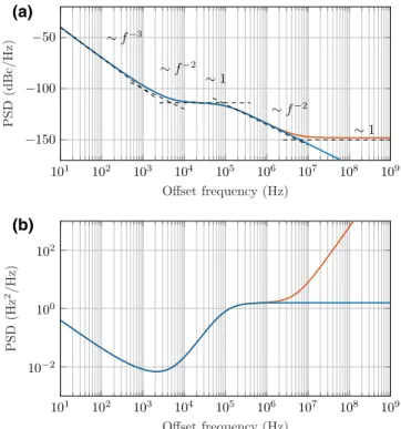
Consider, as an example, the typically reported plot for the phase noise of a phase-locked-loop- (PLL) based frequency generator, as shown in Fig. 3 (cf. Ref. [75]).
Appended to this figure is a plot of the resulting frequency- noise PSD. At low frequencies, the phase noise is typically limited by the flicker noise of the reference clock (which is proportional to the f −3part). In the plot of the frequency- noise PSD, this has a f −1roll-off, making it important to maximizeωmin, which could be resolved by using dynam- ical decoupling schemes, as they introduce an additional high-pass filtering [28,29,76,77]. The part of the phase- noise plot highlighted in red may be a source of concern [26], as it results in a frequency noise increasing as f 2 that exactly cancels the roll-off of the intrinsic qubit fil- ter [Fig.2(a)], thus resulting in a diverging integral for the fidelity (TableI) in the case in which no additional band- pass filtering is applied. However, the noise highlighted in red, visible in the phase-noise plot, originates from thermal noise added to the microwave signal by, e.g., the out- put driver of the microwave signal generator [75,78]. The additive noise, with generally a wide bandwidth, is more accurately modeled in the applied microwave magnetic
field as follows:
B(t)= 2ωR
γe
cos[ωmwt+φ+φn(t)]+Badd(t), (5) where Badd(t) represents the additive noise with PSD Sadd(ω). The actual phase noiseφn(t), indicated by the blue line in Fig. 3, is clearly band limited by the qubit-filter function due to the absence of the f2factor. The PSD of this additive noise has the same frequency dependence as the PSD of the phase noise [79]. The fidelity of the qubit
101 102 103 104 105 106 107 108 109
−150
−100
−50 ∼f−3
∼f−2
∼1
∼f−2
∼1
Offset frequency (Hz)
PSD(dBc/Hz)
(a)
(b)
101 102 103 104 105 106 107 108 109 10−2
100 102
Offset frequency (Hz) PSD(Hz2/Hz)
FIG. 3. A typical plot of (a) the phase noise and (b) the result- ing frequency-noise PSD of a PLL-based frequency generator.
The red line indicates the noise as measured by a phase-noise analyzer, whereas the blue line indicates the part of the noise that is actually phase noise. At high offset frequencies, where the lines diverge, wide-band additive noise shows up in the phase- noise plot, giving rise to a noise floor of around−150 dBc/Hz in this example.
operation in the presence of this type of noise is given in TableI.
Finally, the signal duration T is also subject to random variations, i.e., jitter. However, since the period cannot vary during the operation, the noise in the timing can be simply treated considering the period jitter as a quasistatic error. This period jitter is determined by the single-side- band phase noise Sφ(ω)of the reference clock (period Tclk) used to set the duration [75,80] (TableI), following a high- pass filter (HPF) characteristic with the corner frequency set by the duration T.
B. Specifications for the idle operation and qubit-frequency multiplexing
In a typical quantum algorithm, a qubit can be idle for a while, waiting for the operations on other qubits to fin- ish, before being operated on, e.g., due to limitations in the hardware or data dependencies. This section discusses pro- cesses that cause the state of the qubit to degrade during an idle period lasting Tnop. The loss of the quantum state due to interactions with other qubits will be discussed in Sec.V B.
A qubit will perform an undesired Z rotation (related to T2∗) in the rotating frame if the microwave frequency is not matched to the qubit’s Larmor frequency, even when the driving tone is not applied to the qubit. Evaluating the fidelity of an identity operation in the case of a frequency inaccuracy ωmw,0 leads to FInop,mw =1−14ω2mw,0T2nop, which can easily be more stringent than the requirement due to a rotation (TableI).
Besides Z rotations, unintended X and Y rotations of the qubit (related to T1) are possible in the case in which power is present at the qubit’s Larmor frequency. In general, a tone could be present at the qubit frequency, e.g., due to signal leakage from the microwave source or nonlineari- ties in the system leading to harmonic or intermodulation tones. The presence of a spurious tone that would give a Rabi frequency ofωspurwill reduce the fidelity as follows:
FInop,spur =1−14ω2spurTnop2 .
Besides a tone, residual thermal noise could be present on the drive line. Considering a noise signal with spectral density SRn(ω), the fidelity is FInop,noise =1− (1/π)∞
0 SRn(ω)|Hn(ω)|2dω, where
|Hn(ω)|2=2 sin2
Tnop
2 (ω−ω0)
(ω−ω0)2 , (6) which indicates that the noise spectrum is filtered by a sinc-shaped band-pass filter centered aroundω0, with the following brick-wall approximation:
|Hn(ω)|2≈
T2nop/2, |ω−ω0| ≤π/Tnop,
0, elsewhere. (7)
Lastly, multiple qubits sharing the same control line, i.e., a single ESR line or control gates shorted together, can be controlled independently in the case in which each qubit has a unique Larmor frequency, as mentioned in Sec.II. This technique constitutes FDMA. However, when rotating a qubit with Larmor frequency ω0 by applying a microwave signal at frequency ωmw=ω0, any unad- dressed qubit on the same line with Larmor frequency ω0,other =ω0+ω0,space will be affected. Similarly, even if not on the same drive line, another qubit could be uninten- tionally driven due to parasitic coupling such as capacitive or magnetic cross talk.
An expression for the fidelity of the unaddressed qubit with respect to the ideal identity operation is reported in the Supplemental Material [69] for a microwave pulse with a rectangular envelope [Fig. 4(a)] and it is plotted in Fig. 4(c), where we assume the same Rabi frequency ωR for both qubits. As expected, driving the qubit with a larger amplitude (i.e., largerωR) results in a shorter pulse for a given rotation angle, thus leading to a wider pulse bandwidth and, consequently, to a cross talk extending to qubits that are further away in frequency.
Although the expectation may arise that reducing the pulse bandwidth by proper engineering of the pulse enve- lope can lead to lower cross talk, Fig. 4(d) shows that also a Gaussian envelope [Fig. 4(b)] does not result in a much faster roll-off. As the figure shows, the fidelity can be limited by unintended Z rotations of the unaddressed qubit. However, by applying a simple correction for the Z rotation, the fidelity of the identity operation on the unaddressed qubit improves to the following:
FIFDMA ≈1− β2 α2sin2
θ 2α
≥1−β2
α2, (8)
where α=ω0,space/ωR and β=ωR,unaddressed/ωR and where, in general, the unaddressed qubit can have a differ- ent Rabi frequency (ωR,unaddressed) at the same microwave amplitude, e.g., due to a lower coupling to the drive signal.
As expected, the fidelity given by Eq.(8)is approximately proportional to the spectrum of the envelope of the applied pulse [Fig. 4(c)]. Consequently, reduction of the pulse bandwidth by proper engineering of the pulse envelope is an effective solution if the unintended Z rotations are corrected, as shown in, e.g., Figs.4(b) and4(d), where a Gaussian envelope is employed.
A certain minimum frequency separation is necessary to achieve a target fidelity, as shown in Fig.4(e)for the rect- angular envelope. The lower bound on the fidelity as given in Eq. (8) is plotted as well, as the notches in the graph move depending on θ. Similarly, if the coupling of the microwave drive is due to parasitic effects and is unwanted, a target fidelity for unaddressed qubits translates into a
θ/ωtR
ω/ωR
0 0.1 0.2 0.3 0.4 0.5 0.6 0.7 0.8 0.9 1 0
1 2
θ/ωtR
ω/ωR
10−1 100 101 102
10−4 10−3 10−2 10−1 100
ω0,space/ωR
1−F
FDMA with Rectangular envelope (θ= )
Fidelity
|x|2+|y|2
|z|2
Fourier transform
10−1 100 101 102
10−4 10−3 10−2 10−1 100
ω0, /ωR
1−F
FDMA with Gaussian envelope (θ= )
Fidelity
|x|2+|y|2
|z|2
Fourier transform
100 101 102
10−6 10−5 10−4 10−3 10−2 10−1 100
ω0, /ωR
1−F
Rectangular envelope: ω0,spacerequirement (θ= ) β= 1 β= 0.1 β= 0.01
100 101 102
10−2 10−1 100
ω0, /ωR
β
Rectangular envelope: βrequirement (θ= )
F = 99.999%
F = 99.99%
F = 99.9%
(a) (b)
(c) (d)
(e) (f)
space
space space
FIG. 4. Qubit-frequency multiplexing: the envelopes, achievable fidelity, and requirements in the case of a rectangular envelope.
(a) The rectangular envelope under consideration. (b) The Gaussian envelope under consideration. (c) The infidelity of an identity operation (and the amount of X or Y rotation and Z rotation) on a qubit spaced atω0,spacefrom the carrier for a rectangular envelope, along with the Fourier transform of the rectangular envelope. (d) The infidelity of an identity operation (and the amount of X or Y rotation and Z rotation) on a qubit spaced atω0,spacefrom the carrier for a Gaussian envelope, obtained by numerical simulation, along with the Fourier transform of the Gaussian envelope. (e) The frequency spacing required to achieve a certain fidelity at given relative signal strengthβ, for a rectangular envelope. The upper bound (dashed lines) is given in Eq.(8). (f) The driving tone attenuationβ required at a certain frequency spacing to achieve a given fidelity, for a rectangular envelope. The lower bound (dashed lines) is given in Eq.(9).
requirement in the driving tone attenuation [Fig.4(f)]:
β =
1−Fcorr
α sin
θ 2α
≥
1−Fcorr
ω0,space
ωR
. (9)
Finally, FDMA has the potential to perform single-qubit gates on several qubits at the same time, using a sin- gle drive line. In that case, it is not sufficient to apply a compensating Z rotation afterward, on another qubit, if that qubit is also performing an operation. As the Z
rotation is obtained gradually when an off-resonance tone is applied, the driving tone applied to perform the oper- ation should be altered to compensate for this Z rotation during the operation. This requires proper engineering of all the microwave pulses that are applied simultaneously [37,81–84].
C. Case study of the specifications for a single-qubit operation
With the information provided in Sec.IV, clear specifi- cations for the control electronics can be derived. TableII shows as an example of how the total error budget can be allocated over the electronics specification to achieve a 99.9% fidelity for aπ rotation at a Rabi frequency of 1 MHz. The same fidelity is targeted for preserving the state of the qubit when not operating on it for a time equal to the operation time (Tnop=T). The example considers the use of simple rectangular pulses, without any echo technique.
A Larmor frequency larger than 80 MHz would be sufficient not to get impaired by fast-oscillating terms neglected by the rotating-wave approximation (RWA, see the Supplemental Material [69]). However, choosingω0= 10 GHz is more in line with values used in practice and allows for a large qubit-frequency spacing. A frequency spacing of 1 GHz is selected, the same as considered in the case study of two-qubit operations (Sec. V C). Such spacing is, however, approximately 10 times larger than required for minimizing the cross talk due to FMDA
(Sec.IV B). The example also shows the effect of the fre- quency noise as expected from isotopically purified Si-28 (800 ppm 29Si), highlighting that its contribution to the infidelity is negligible in this example.
The values provided for the microwave amplitude assume a qubit plane based on EDSR, where an ampli- tude of 2 mV at the gate is required for a Rabi frequency of 1 MHz (close to the value reported in Ref. [44]). All specifications are valid at the gate, so that wiring attenua- tion and filtering might need to be factored in to refer the specifications back to the electronics.
Following these specifications, the microwave envelope (amplitude and duration) can be generated by, e.g., an AWG with a sample rate of at least 150 megasamples/s (MS/s), such that the sample time is less than 6.7 ns, result- ing in a maximum inaccuracy of 3.3 ns. Furthermore, the AWG should have a resolution of 8 bits, such that at a full- scale swing of 4 mV, the quantization step is sufficiently low. To meet the noise requirement and the specifications on the residual driving when not operating the qubit (“Off spur” in TableII), an effective number of bits (ENOB) of only 6.5 bits is required.
The LO used for the up-conversion requires a fre- quency resolution of approximately 20 kHz (for the inac- curacy). Assuming a −20 dB/dec slope of the phase noise, the single-side-band phase noise at 1 MHz from the carrier,L(1 MHz), needs to be below−106 dBc/Hz.
Furthermore, the LO’s phase inaccuracy needs to be below 0.64◦.
TABLE II. Example specifications for the control electronics for single-qubit operations. The PSD values provided as a comment assume a white spectrum for the amplitude and frequency noise (i.e.,−20 dB/dec for the phase noise).
Infidelity contribution
Value To an operation To idling Comment Frequency
Nominal 10 GHz 0.64×10⁻⁹ RWA when driving a qubit
Spacing 1 GHz 1×10⁻⁶ FDMA leakage with rectangular envelopes
Inaccuracy 11 kHz 125×10−6 308×10−6
Oscillator noise 11 kHzrms 125×10−6 308×10−6 ENBW = 2.5 MHz,L(1 MHz)= −106 dBc/Hz Nuclear spin noise 1.9 kHzrms 3.6×10⁻⁶ 8.9×10⁻⁶ From Ref. [45], T2∗=120μs
Wide-band noise 12μVrms 125×10−6 ENBW = 2.9 MHz, Sadd=7.1 nV/√ Hz Phase
Inaccuracy 0.64◦ 125×10−6 31×10−6 FDMA Z corrections limit the no operation Amplitude
Nominal 2 mV Full scale: 4 mV, rms: 1.4 mVrms
Inaccuracy 14μV 125×10−6
Noise 14μVrms 125×10−6 ENBW = 1.0 MHz, PSD=14 nV/√
Hz, SNR= −40 dB
Off spur 19μV 217×10−6 −41 dBc
Off noise 10μVrms 125×10−6 ENBW = 2.0 MHz, PSD=7.1 nV/√
Hz Duration
Nominal 500 ns
Inaccuracy 3.6 ns 125×10−6
Noise 3.6 nsrms 125×10−6
FX ,Y=99.9% FI =99.9%
−1 −0.5 0 0.5 1 0
2 4
×1011
/U
Energy(arb.units)
Energy-Level Diagram
t0= 0 t0>0
−999t0n−990t0n−900t0n
0 900t0n990t0n999t0n
0.01t0n
0.1t0n
t0n
103 105 107 109
Detuning energy Tunnel coupling
ωop
The operation speed ωop(U= 1000t0n)
(a) (b)
FIG. 5. (a) The energy-level diagram of the two-qubit system. An avoided crossing is visible for|| =U when there is a finite tunnel coupling between the dots. (b) The two-qubit operation speedωop[Eq.(11)] versus the interdot tunnel coupling and detuning.
A nominal tunnel coupling t0nof 1 GHz is used.
V. SIGNAL SPECIFICATIONS FOR TWO-QUBIT OPERATIONS
A. Fidelity of a two-qubit operation
As stated in Sec. II, by default the tunnel coupling between the qubits is negligible and the qubits have the same potential, i.e., they are not detuned. By increasing the tunnel coupling and/or by detuning the qubits, the qubit interaction increases and a two-qubit gate can be obtained.
In this system, by leveraging this exchange interaction, a two-qubit exchange gate and a C phase gate can be implemented. With either of these gates and single-qubit operations, a universal set is obtained.
To describe the physical interactions required for the two-qubit gate, higher energy levels need to be mod- eled in the Hamiltonian. The analysis presented here is limited to the interaction between two neighboring qubits, A and B, and to the single-dot singlet states (|0, 2 represents the singlet state in the right dot and
|2, 0 the singlet state in the left). In the basis = [|↑,↑,|↑,↓,|↓,↑,|↓,↓,|0, 2,|2, 0], the Hamilto- nian of a double quantum dot is given by the following (=1) [55,85,86]:
H =
⎡
⎢⎢
⎢⎢
⎢⎢
⎢⎢
⎣
−ω0 0 0 0 0 0
0 δω0
2 0 0 t0 t0
0 0 −δω0
2 0 −t0 −t0
0 0 0 ω0 0 0
0 t0 −t0 0 U− 0
0 t0 −t0 0 0 U+
⎤
⎥⎥
⎥⎥
⎥⎥
⎥⎥
⎦ ,
(10)
whereω0=(ω0,A+ω0,B)/2,δω0=ω0,B−ω0,A, andω0,A
andω0,Bare the Larmor frequencies of the two qubits. The charging energy (U) is assumed to be the same for both dots. The tunnel coupling between the quantum dots (t0) has an exponential relation to the voltage on the barrier gate and the detuning energy () is controlled by the volt- age difference on the plunger gates of the dots (Vd) via the lever armα=/Vd.
An avoided crossing is observed in the energy-level diagram for || =U and t0>0 [Fig. 5(a)], which gives rise to eigenenergies that are different from the case of two isolated dots (t0∼0) for any detuning. This change of eigenenergy and the corresponding eigenstate form the basis of the two-qubit operations. An investigation of the eigenenergies of the Hamiltonian in Eq. (10) reveals that the total change in eigenenergy equals the following (=1):
ωop=4t20 U
U2−2. (11)
Note that the expression used in this paper forωopderives directly from the Hamiltonian of Eq.(10). However, exper- iments have reported ωop as an exponential function of detuning [87].
Asωopdescribes the amount of exchange interaction, it directly sets the speed of the two-qubit operation. A plot ofωop versus the tunnel coupling and detuning is shown in Fig.5(b). To perform the two-qubit operation, a control pulse must be applied, to move the system away from the default point (negligible tunnel coupling and zero detun- ing) to the desired operating point, where there is sufficient exchange interaction such that a two-qubit operation is per- formed. From Fig.5(b), it is clear that a fast gate can be