the iridium L‑edges for the Athena silicon pore optics reflector
Author Hisamitsu Awaki, Yoshitomo Maeda, Hironori Matsumoto, Sara Svendsen, Marcos Bavdaz, Maximilien Collon, Kazunori Asakura, Finn E.
Christensen, Desiree D. M. Ferreira, Matteo Guainazzi, Masato Hoshino, Shuntaro Ide,
Kazunori Ishibashi, Wansu Kan, Sonny Massahi, Takuya Miyazawa, Sadayuki Shimizu, Brian
Shortt, Yusuke Takehara, Keisuke Tamura, Kentaro Uesugi, Richard Willingale, Tomokage Yoneyama, Atsushi Yoshida
journal or
publication title
Journal of Astronomical Telescopes, Instruments, and Systems
volume 7
number 1
page range 014001
year 2021‑01‑06
Publisher SPIE
Rights (C) The Author(s).
Author's flag publisher
URL http://id.nii.ac.jp/1394/00001891/
doi: info:doi/10.1117/1.JATIS.7.1.014001
Creative Commons Attribution 4.0 International(https://creativecommons.org/licenses/by/4.0/)
L-edges for the Athena silicon pore optics reflector
Hisamitsu Awaki,a,* Yoshitomo Maeda,b Hironori Matsumoto,c Sara Svendsen ,d Marcos Bavdaz,e Maximilien Collon ,f Kazunori Asakura,c Finn E. Christensen,d Desiree D. M. Ferreira ,d Matteo Guainazzi,eMasato Hoshino,gShuntaro Ide,c Kazunori Ishibashi,h Wansu Kan,a Sonny Massahi ,d Takuya Miyazawa,i Sadayuki Shimizu,h Brian Shortt,e Yusuke Takehara,h Keisuke Tamura,j Kentaro Uesugi,g
Richard Willingale,k Tomokage Yoneyama,c and Atsushi Yoshidah
aEhime University, Faculty of Science, Matsuyama, Japan
bInstitute of Space and Astronautical Science, Japan Aerospace Exploration Agency, Sagamihara, Japan
cOsaka University, Graduate School of Science, Osaka, Japan
dTechnical University of Denmark, DTU Space, National Space Institute, Lyngby, Denmark
eEuropean Space Research and Technology Centre, Noordwijk, The Netherlands
fcosine, Warmond, The Netherlands
gJapan Synchrotron Radiation Research Institute/SPring-8, Sayo, Japan
hNagoya University, Graduate School of Science, Nagoya, Japan
iOkinawa Institute of Science and Technology Graduate University, Okinawa, Japan
jNASA Goddard Space Flight Center, Greenbelt, Maryland, United States
kUniversity of Leicester, Department of Physics and Astronomy, Leicester, United Kingdom Abstract.Athena, a future high-energy mission, is expected to consist of a large aperture x-ray mirror with a focal length of 12 m. The mirror surface is to be coated with iridium and a lowZ overcoat. To define the effective area of the x-ray telescope, the atomic scattering factors of iridium with an energy resolution less than that (2.5 eV) of the x-ray integral field unit are needed. We measured the reflectance of the silicon pore optics mirror plate coated with iridium in the energy range of 9 to 15 keV and that near the iridium L-edges in steps of 10 and 1.5 eV, respectively, at the synchrotron beamline SPring-8. The L3, L2, and L1 edges were clearly detected around 11,215, 12,824, and 13,428 eV, respectively. The measured scattering factors were∼3%smaller than the corresponding values reported by Henke et al., likely due to the presence of an overlayer on the iridium coating, and were consistent with those measured by Graessle et al. The angular depend- ence of the reflectivity measured indicates that the iridium surface was extremely smooth, with a surface roughness of 0.3 nm.©The Authors. Published by SPIE under a Creative Commons Attribution 4.0 Unported License. Distribution or reproduction of this work in whole or in part requires full attribution of the original publication, including its DOI.[DOI:10.1117/1.JATIS.7.1.014001]
Keywords:x-ray optics; Athena; silicon pore optics; atomic scattering factors; iridium.
Paper 20119 received Aug. 4, 2020; accepted for publication Dec. 16, 2020; published online Jan. 6, 2021.
1 Introduction
The Advanced Telescope for High-Energy Astrophysics (Athena)1 is a next-generation x-ray telescope to be developed by the European Space Agency (ESA) as a part of its Cosmic Vision L2 program. Athena is expected to operate in the energy range of 0.2 to 12 keV and realize the advanced x-ray imaging and spectroscopy of the hot Universe. The key scientific objectives are to determine how and when large-scale hot gas structures formed in the Universe, to perform a complete census of black hole growth in the Universe, and explore high-energy phenomena, which are expected to provide a valuable basis for astrophysics research in the 2030s.
*Address all correspondence to Hisamitsu Awaki,[email protected]
Athena is expected to consist of a large aperture x-ray mirror2with a focal length of 12 m and a goal of an on-axis angular resolution of 5 arc sec half energy width (HEW). The focal plane contains two instruments: a wide field imager3and an x-ray integral field unit (X-IFU).4In the design of the large aperture telescope, a considerably high ratio of the collecting area to the mass is realized by employing ESA’s silicon pore optics (SPO) technology. This SPO telescope adopts Wolter-I type grazing optics,5and in the current baseline coating design, the reflector surface is expected to be coated with iridium. The large aperture telescope will be composed of∼700SPO modules, with each mirror module containing 70 mirror plate pairs.2The effective area of the Athena telescope is to be determined by summing the geometrical area times the individual reflectance of each module based on the telescope design. Specifically, to define the effective area in the high-energy region, it is necessary to ensure a suitable reflectance near the iridium L- edges. Because the X-IFU is designed to realize spatially resolved high-resolution spectroscopy with an energy resolution of 2.5 eV,4the reflectance should be determined with an energy pitch of <2.5 eVto suitably define the effective area. Henke et al.6determined the atomic scattering factors for various elements at an energy range of 10 to 30,000 eV. However, Henke et al.’s data6 were based on the empirical cross section by Biggs and Lighthill7above 10 keV. Thus, the opti- cal constants of iridium near L-edges are not reproduced in the energy resolution of the transition edge sensor (TES) of the X-IFU. Therefore, it is necessary to measure the reflectance of the SPO mirror with an energy pitch smaller than the spectral resolution of the X-IFU.
In the previous work, ground calibration was performed, and the x-ray properties of x-ray mirrors were clarified. Specifically, iridium optical constants for the Chandra x-ray observatory were measured in the energy band from 50 to 12000 eV8to tabulate the iridium optical constants over the full range for this observatory. Kikuchi et al.9measured the atomic scattering factors around the gold L-edges for the ASTRO-H (Hitomi)10 telescope with a sub-eV energy pitch matching the spectral resolution (∼5 eV) of the microcalorimeter soft x-ray spectrometer.11,12 To identify the x-ray property of the SPO mirror covering the energy range of Athena, we attempted to perform the x-ray measurements in the high-energy region from 9000 to 15,000 eV at the synchrotron radiation facility SPring-8. A preliminary optical study is shown by Massahi et al. (in prep) where the absorption edges of single-layer iridium in the energy range from 50 to 800 eV are presented. Here, two techniques were used: x-ray reflectivity (XRR) and x-ray photo- electron spectroscopy (XPS) to identify the absorption edges and emission lines of the material.
It was shown that the surface of iridium film was contaminated with hydrocarbons displaying C and O K edges. We also expect these contaminants on the iridium film investigated in this work.
Section2 provides the SPO mirror sample, facility of the x-ray beam line, and the method to measure the x-ray reflectance. Section3 presents results of the reflectance measurements with angle scan and energy scan. The scattering factorsf1 andf2 are estimated from our measure- ments in Sec.4. In the estimation, we first employ a single-layer model to the measured reflec- tance and then employ an overlayer model as considered by Graessle et al.8This paper presents our findings pertaining to the atomic scattering factors for iridium (and at all its L-edges) in the high-energy region.
2 SPO Mirror Plate and X-Ray Measurement 2.1 SPO Mirror Plate
SPO mirror plates are used to manufacture the SPO stacks, which are integrated in pairs in the mirror modules for the Athena optics. The mirror substrate is made from commercially available silicon wafers.13The plate consists of two main functional parts: a membrane, which acts as the mirror, and ribs to interconnect multiple plates. To implement the Wolter-I type configuration of the stacked plates, an oxide wedge is grown along the ribbed direction of the SPO plate.
The complete process to create the pore structure from silicon wafers has been described by Landgraf et al.14
The SPO plate considered in this study was diced to create a rectangular shape with a length and width of 110 and 49 mm, respectively, corresponding to the inner radius modules of the Athena optics. For the purpose of coating characterization, the substrate surface has no
photoresist patterning. The sample was prepared at the coating facility dedicated for the Athena mirror production.15Specifically, the substrates were plasma cleaned prior to being coated, using the integrated inverse sputter etcher to remove any surface contamination and ensure a smooth surface. A 10-nm-thick iridium thin film coating was deposited using dc magnetron sputtering at a working pressure of3.4×10−3 mbarand magnetron discharge power of 1860 W. A honey- comb collimation mesh was placed in the path between the iridium target and substrate to min- imize the coating roughness.
2.2 SPring-8
We performed x-ray measurements of the SPO plate from January 18–22, 2019, at BL20B216in SPring-8, which is a third-generation synchrotron radiation facility located in Hyogo, Japan. The acceleration energy of the electron beam was 8 GeV.
In general, BL20B2 is a medium-length beamline with a bending magnet as a light source, which is allocated for medical applications and developments of various imaging techniques in the energy range of 5 to 113 keV. The total length of this beamline is 215 m (from light source to end station). BL20B2 consists of an optics hutch and three experimental hutches 1, 2, and 3 located 42, 200, and 207 m from the light source, respectively. The x-ray beam, which is extracted from the bending magnet with a horizontal acceptance angle of 1.5 mrad, spreads to a 300-mm- wide beam at hutch 2; therefore, the available maximum x-ray beam size is 300 mm (horizontal)× 20 mm (vertical). The Si double crystal monochromator (DCM),17which monochromatizes con- tinuum x-rays, is located in the optics hutch, 36.8 m from the light source. By changing the crystal planes of 111 (5.0 to 37.5 keV), 311 (8.4 to 72.5 keV), and 511 (13.5 to 113.3 keV), a wide energy range (5 to 113 keV) is available. In our experiment, we selected the crystal plane of 311. The energy resolution (ΔE∕E) of the available x-ray beam is <10−4 in this energy region.
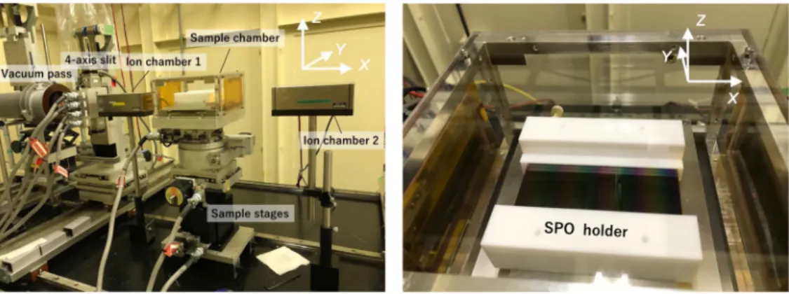
Figure1 shows the SPO plate placed in hutch 3. The x-rays arrived from the left side of Fig.1. The direction of the x-ray beam and that perpendicular to the x-ray beam were defined as the X and Z axes, respectively. The sample chamber, which included the SPO plate, was mounted on the positioning stages, which allowed three-axis rotations (θX,θY, and θZ) and two-axis translations (Yand Z). The SPO plate was set in the sample chamber using an SPO holder made of Teflon. To monitor the intensity of the x-ray beam, an ionization chamber (IC1) was present in the front of the sample chamber. Moreover, another ionization chamber (IC2) was set behind the SPO sample to measure the intensity of the reflected x-rays.
The x-ray beam was shaped to a size of 0.03 mm (vertical)×0.5 mm (horizontal) by the four- axis slits in the front of IC1. Since the divergence angle of the shaped x-ray beam at 200 m from the light source was <1 arc sec, the beam size at IC2, which was located about 0.6 m behind the four-axis slit, is similar to the slit size.
Although air was used in IC1, argon was used instead of air to increase the detection effi- ciency in IC2. IC1 and IC2 had the same geometrical structure with horizontally long windows sized 8 mm (vertical)× 65 mm (horizontal). The reflected beam was moved into the vertical
Fig. 1 Images of the experimental setup. The right image shows the inside of the sample chamber.
direction (Z) by changing the incident angle to the SPO sample. The vertical displacement of the beam at the entrance of IC2 was about 6.6 mm per degree of incident angle. IC2 was rotated 90 deg around the Xaxis so that the long direction of entrance window was vertical.
2.3 X-Ray Measurements to Determine the Reflectance
The reflectanceRis defined as the ratio of the intensity of a reflected x-ray to that of the incident x-rays. Because the intensity of the incident x-rays may fluctuate, and IC1 and IC2 detect back- ground events, we subtracted the background events and then corrected the fluctuation of the incident x-rays. After incorporating the corrections, the reflectance can be defined as
EQ-TARGET;temp:intralink-;e001;116;615
R¼ðI2r−I2bÞðI1d−I1bÞ
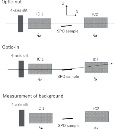
ðI2d−I2bÞðI1r−I1bÞ; (1) whereI1andI2denote the output counts of IC1 and IC2, respectively; and the subscriptsd,r, and bdenote the incident x-rays, reflected x-rays, and background, respectively (see Fig. 2).
In the case of our IC, the current from the IC was amplified with a transconductance (current to voltage) amplifier, and it was converted to pulses with a voltage to frequency (V∕F) converter and counted by a scaler. At the transconductance amplifier, we added an offset voltage to avoid a negative output. Thus, the outputs from IC1 and IC2 contain the offset at the transconductance amplifier, and the value obtained by subtracting the offset from the output of IC is proportional to the intensity of the incident x-ray.
In general, the reflectanceRis described as a function of the energyEof the incident x-ray and grazing angleθ. Therefore, we measured the reflectivity by performing angle and energy scans at fixed energies and fixed incident angles, respectively.
The angle scans were performed to determine the surface roughness (σ), thickness (d) of the iridium coating, interfacial roughness (σb) between the iridium layer and mirror substrate, and
Fig. 2 Schematic of the configuration for each measurement. In the background measurement, the beam shutter upstream of the beam line was closed. The x-ray beam was shaped with the four- axis slit to a size of 0.03 mm (vertical)×0.5 mm (horizontal).
the atomic scattering factorsf1andf2of iridium. Angle scans were performed at x-ray energies of 11, 12, and 14 keV, spanning the range of the iridium L-edges,6,18 specifically, the L3 edge (11.21520.0003 keV), L2 edge (12.82410.0003 keV), and L1 edge (13.4185 0.0003 keV). The incident angle was scanned up to 1.5 deg in steps of 0.05 deg measure the thickness of the iridium layer.
The energy scans were performed to measure the energy dependence of the atomic scattering factors with an exposure time per point of 3 s. The wide energy region covering the iridium L-edges was scanned in two energy ranges: 9 to 13 keV and 12 to 15 keV in steps of 10 eV.
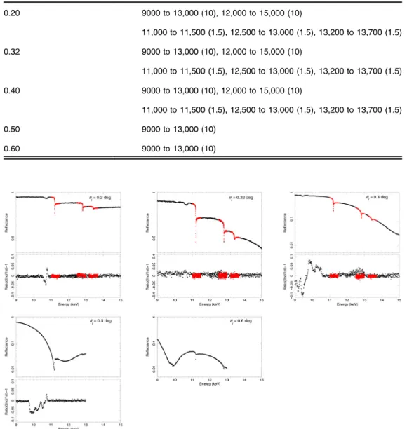
This scan was referred to as a coarse pitch scan in this work. Furthermore, energy scans were performed around the energies of the iridium L-edges in steps of 1.5 eV to clarify the iridium L- shell structure off1andf2. The energy step was smaller than the energy resolution of the X-IFU TES detector onboard Athena. This scan was referred as a fine pitch scan in this work. The incident angles in the energy scan were selected as 0.20 deg, 0.32 deg, 0.40 deg, 0.50 deg, and 0.60 deg to include the critical angles at 9 and 15 keV. However, owing to machine-time lim- itations, only the energy region of 9 to 13 keV was covered at incident angles of 0.50 deg and 0.60 deg.
3 Results of the Reflectance Measurement
3.1 Characteristics of the Background of the Ionization Chamber
The background outputs of IC1 and IC2,I1bandI2b, which were measured before/after the angle and energy scans, were used to evaluate the stability of the background outputs of IC1 and IC2.
Figure3shows the mean intensities of the backgrounds for each 3 s as a function of the elapsed time from 0:00 [Japan Standard Time (JST) (= UTC + 9 h)] on January 20, 2019. The uncertainty is defined as the standard deviation of 5 or 20 background data points.I1b and I2b gradually decreased at ΔI∕Δt¼−0.708and −1.458 counts∕3 s h−1, respectively. The time drift of the background intensities during each scan (Δt<2 h) was comparable with or less than the stat- istical uncertainty. Thus, the derived standard deviations were used asI1bandI2b. Because no background measurements were performed before and after the energy scans atθ¼0.32 deg and 0.40 deg, the average background outputs of IC1 and IC2, which were estimated to be 268.8 and 480.5, respectively, were applied for I1b andI2bin the energy scans.
Fig. 3 Variability in the background intensitiesI1bandI2b. The uncertainties in these intensities are defined as the standard deviations of 5 or 20 measurements. A log of the scans in the experi- ment is presented above the figure.
3.2 Energy Calibration
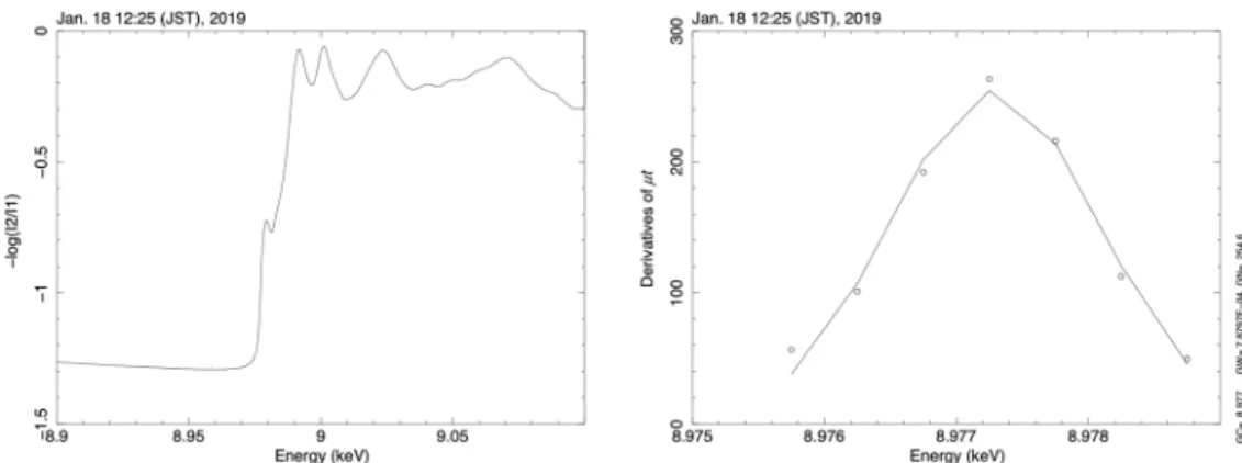
To calibrate the energy scale, a thin Cu foil was placed on the window on the downstream side of IC1. Subsequently, we measured the output counts of IC1 and IC2 in the energy range from 8.9 to 9.1 keV with a step of 0.5 eV. The exposure time was 1 s, and the vertical slit size was30μm.
The energy calibration was performed four times during the experiment. Figure 4 shows
−logðI2∕I1Þ as a function of the energy; the value of −logðI2∕I1Þ corresponds toμt, where μand t denote the absorption coefficient and Cu foil thickness, respectively. The absorption edge energy was defined as the energy with the maximum derivative ofμt. In the fitting with a Gaussian model, the peak value was 8977.3 eV (right panel in Fig.4). All of the energy cal- ibration data points were treated in the same manner, and all the peak energies were noted to be consistent within 0.1 eV. Table1presents the results of the energy calibrations. The peak energy is identified as that of the Cu K pre-edge (8980.4 eV).19Thus the peak energy was−3.1 eVless than the energy of the pre-edge. This offset was corrected to assume a fixed angular offset of 0.009 deg in the angle of the DCM.
3.3 Calibration of the Incident Angle
The incident angle to the SPO plate was changed by operating the swivel stage in the sample stages, and it was calibrated by obtained an x-ray image of the reflected light using an sCMOS- based visible light conversion type x-ray image detector (sCMOS). The sCMOS was placed 2362 mm from the center of the SPO plate. A narrow beam with dimensions of 0.03 mm (Z) and 5 mm (Y), respectively, was reflected on the SPO plate at a swivel ofθY. Using the sCMOS, we measured the beam displacement between the reflection and translating the optic out of the beam. The incident angle θI was calculated from the displacement and the relation between θI andθY was determined. In the angle scan, we estimatedθI using this relation, whereas in the energy scan,θI was fixed using the sCMOS.
Fig. 4 Transmissivity of the Cu thin foil.−logðI2∕I1Þin the left panel corresponds toμt, where μand t denote the absorption coefficient and absorber thickness, respectively. The maximum derivatives ofμt were obtained by fitting with a Gaussian model.
Table 1 Energy calibration results.
Time and date (JST) Peak energy (eV)
12:25; January 18, 2019 8977.3
21:00; January 19, 2019 8977.3
13:05; January 20, 2019 8977.4
04:45; January 21, 2019 8977.3
3.4 Reflectance Obtained from the Angle Scan
Before starting the angle scan, the outputs in optic-out (I1dandI2d) and backgrounds (I1band I2b) were obtained five times. The mean values of the outputs were calculated for estimating the reflectance using Eq. (1). Figure5 shows the reflectance as a function ofθI. The interference fringes resulting from a thin iridium layer with a thickness of∼10 nmwere observed at large incidence angles. To verify the consistency between the angle and energy scans, the results obtained using the energy scan were plotted (red open squares in Fig.5). A reasonable agreement between the two scans can be observed.
Next, we estimated the error on the reflectance. The outputs,I1randI2rin optic-in could not follow Poisson statistics, because we added the offset at the transconductance amplifier. Since the output of IC2 in optic-in consists of two components, outputs of IC2 in beam off and outputs originated from the reflected light. The error on the former component was estimated as the standard deviation on the background output, and the error on the latter component could be expressed by the statistical error on the measured x-ray intensity. Specifically, the errors ΔI1r andΔI2rcould be represented as
EQ-TARGET;temp:intralink-;e002;116;400
ΔI21r¼ΔI21bþa21ðI1r−I1bÞ ΔI22r¼ΔI22bþa22ðI2r−I2bÞ
; (2)
wherea1anda2are the factors representing the statistical error on the x-ray intensity. The factors were estimated from the outputs in optic-out. For instance,ΔI21d¼ΔI21bþa21(I1d−I1b), where ΔI1d andΔI1bare the standard deviations of the five measurements before starting the angle scan. The factors a21 and a22 depend on the x-ray energy.a21 atE¼11, 12, and 14 keV was calculated as 0.0098, 0.0116, and 0.1269, respectively, anda22atE¼11, 12, and 14 keV was calculated as 0.036, 0.146, and 2.517, respectively. The error on the reflectance was estimated using the error ofI1r and I2r represented in Eq. (2).
3.5 Reflectance Obtained by Performing the Energy Scan
After recordingI1bandI2b20 times, we measured the intensities of the incident x-ray beam,I1d
and I2d, and those of the reflected x-rays,I1r and I2r. The exposure time was 3 s. The mea- surements were conducted two times to evaluate the reproducibility. The measurements were obtained in the following order: optic-out, optic-in, optic-in, and optic-out. However, the first energy scan at θI¼0.6 degfailed owing to issues with the data acquisition. Thus, only the second measurement was considered. The parameters for the energy scan are listed in Table2. Figure6shows the mean reflectance of two measurements obtained in the energy scan.
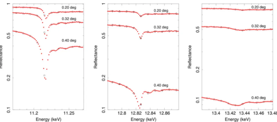
The iridium L-edge structure of the reflectance is shown in Fig.7. In the case of the energy scans atθI¼0.32 degand 0.40 deg, the average backgrounds were adopted asI1bandI2bto derive the reflectance.
The errors on the reflectance at energyEiwere assumed to be reproducibility, which is the variation between the two measurements, and were estimated from the relative deviationδji of each measurementRji (j¼1or 2) from the mean valuemi. The relative deviation was defined as Fig. 5 X-ray reflectance obtained using the angle scan. The x-ray reflectance obtained using the energy scan is plotted as red open squares.
δji ¼ ðRji −miÞ∕mi, whereiis the index of the scan data. The root mean square (rms) ofδiwas considered as the relative error in the reflectance and defined as follows:
EQ-TARGET;temp:intralink-;e003;116;188
RMS¼
ffiffiffiffiffiffiffiffiffiffiffiffiffiffiffiffiffiffiffiffiffiffiffiffiffiffiffiffiffiffiffiffiffiffiffiffiffiffiffiffiffiffi 1
N
Xfðδ1iÞ2þ ðδ2iÞ2g r
; (3)
whereN is the total number of data points. By considering the ratiori (¼R1i∕R2i) of the two measurements of reflectance and considering thatriþ1to 2, the following expression can be obtained
EQ-TARGET;temp:intralink-;e004;116;106ðδ1iÞ2þ ðδ2iÞ2¼2
ri−1 riþ1
2
∼1
2ðri−1Þ2: (4)
Table 2 Parameters for the energy scan.
Incident angleθI (deg) Scanning energy range (step) (eV)
0.20 9000 to 13,000 (10), 12,000 to 15,000 (10)
11,000 to 11,500 (1.5), 12,500 to 13,000 (1.5), 13,200 to 13,700 (1.5)
0.32 9000 to 13,000 (10), 12,000 to 15,000 (10)
11,000 to 11,500 (1.5), 12,500 to 13,000 (1.5), 13,200 to 13,700 (1.5)
0.40 9000 to 13,000 (10), 12,000 to 15,000 (10)
11,000 to 11,500 (1.5), 12,500 to 13,000 (1.5), 13,200 to 13,700 (1.5)
0.50 9000 to 13,000 (10)
0.60 9000 to 13,000 (10)
Fig. 6 Mean reflectance obtained in the energy scan with coarse and fine pitches. The black and red data present the results obtained from the coarse and fine pitch scans, respectively. The ratios between the two measurements are also plotted. In the energy scan atθI¼0.6 deg, the first measurement failed, thus the corresponding ratio is not plotted.
Then
EQ-TARGET;temp:intralink-;e005;116;514
RMS¼
ffiffiffiffiffiffiffiffiffiffiffiffiffiffiffiffiffiffiffiffiffiffiffiffiffiffiffiffiffiffiffiffiffi 1
N
X1
2ðri−1Þ2 r
: (5)
The bottom panels in Fig.6 display the values ofri−1. The data were grouped in 500 eV batches. It was assumed that the relative errors within a data group were the same, and the error was estimated using Eq. (5). The relative errors in the energy region above 11 keV were esti- mated to be∼0.3%to 0.5%. The angle scan data atE¼12 keVwere obtained with an exposure time of 3 s, and the relative error was estimated to be∼0.46%at incident angles below 0.4 deg.
This value is similar to the relative error estimated using Eq. (2).
In the energy region below 11 keV, the ratio deviated from unity. The discrepancy led to the reflectance exhibiting a large error of about 5% at the specific energies Although the underlying cause was not further examined, the large discrepancy may be caused by the contamination with unexpected higher-order x-ray photons to the incident x-rays. In the case ofθI ¼0.32 deg, a small dip at∼10.6 keVwas reproduced in the two measurements. Owing to the reproducibility of the dip structure, the dip structure had small error and affected the calculation of the atomic scattering factors (see Fig.10).
4 Estimating the Atomic Scattering Factors 4.1 Reflectance of a Single Layer
The reflectance from any interface can be calculated using Fresnel’s equations by employing the continuity conditions for incident, reflected, and transmitted waves. Figure8schematically illus- trates a mirror substrate coated with a thin layer with a thicknessd1. The refractive indices of the substrate, thin layer, and medium (air) above the layer are defined asn˜0,n˜1, andn˜2, respectively.
The refractive index of an x-ray with an energyEis expressed as
EQ-TARGET;temp:intralink-;e006;116;185˜
nðEÞ ¼1−δðEÞ þiβðEÞ; (6)
whereδðEÞandβðEÞdenote the dispersion and absorption terms, respectively, and are related to the atomic scattering factors f1 and f2 as
EQ-TARGET;temp:intralink-;e007;116;130
δ¼reN0ρ
2πA λ20f1; β¼reN0ρ
2πA λ20f2; (7)
whereN0is the Avogadro constant,reis the classical electron radius,Ais the atomic weight,ρis the mass density, andλ0 is the x-ray wavelength.
Fig. 7 Iridium L-edge structure of the reflectance obtained by the energy scan. The black circles and red data present the results obtained from the coarse and fine pitch scans, respectively.
The reflectivity coefficientRcan be expressed as
EQ-TARGET;temp:intralink-;e008;116;560
R¼ r1þr0 expð−iΔ1Þ
1þr0r1 expð−iΔ1Þ; (8)
wherer1 andr0 denote the Fresnel reflectivity coefficients of the two interfaces (air/thin layer and thin layer/substrate, respectively).Δ1corresponds to a phase shift;Δ1¼ ð4π∕λ0Þn˜1d1sinϕ. The reflectivity of the thin layer is deduced as a square ofR. If the surfaces of the thin layer and substrate interface are not smooth, the loss of reflectance owing to roughness must be consid- ered. In this work, the Nevot–Croce factor20was considered to take into account the effect of roughness. The reflectance and effect of the roughness were determined using the subroutines multilayerRefl and calcRoughness, of xrtreftable in heasoft 6.25,21respectively.
To determine the optimal parameters that could reproduce the measurements, the MINUIT package developed by CERN to determine the minimum value of a multiparameter function and analyze the shape of the function around the minimum, was used. This software package was used to determine the optimal fit parameters with the minimum value ofχ2.
4.2 Analysis of Angle Scan Data
The fit to the angle scan data was used to identify the parameters describing the iridium layer, specifically, the thickness of the iridium layer (d), interfacial roughness between the iridium layer and SPO substrate (σb), and the surface roughness of the iridium layer (σ). The atomic weights of iridium and the substrate (SiO2) were 192.22 and 60.083, respectively, and the corresponding mass densities were 22.421 and2.65 g cm−3, respectively.
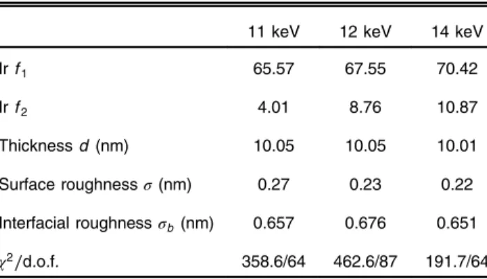
First, we fitted the angle scan data in the angular region between 0.1 deg and 1.5 deg using model 1 in whichσ¼σb. In the fitting procedure,f1andf2of the substrate were set constant as those ofSiO2. Table3lists the best fit parameters, and the best fit model is overlaid on the data with a dashed line in Fig.9. Although the best fit values off1,f2,d, andσwere as expected, model 1 yielded a largeχ2value due to a large discrepancy at the minimum of the interference pattern. Subsequently, model 2, in which the interfacial roughness (σb) was considered to be variable, was used to reproduce the interference pattern. Although the values of χ2 reduced to∼1∕4, the values were still large due to the discrepancy atθI>1 deg(Fig. 9).
Although the measurements forθI>1 degwere effective for reproducing the interference pattern, it was efficient to use the data at the angle near the critical angle to determinef1andf2. The data atθI<0.6 degwere also less affected by background uncertainty. Thus, we fitted the angle scan data at the angular regionθI <0.6 degusing model 2. The best fit iridium thickness involved a large uncertainty because only one interference pattern was present atθI <0.6 deg.
Thus, we fixed the thicknessdas 10.04 nm, which was the mean value of the best fit thickness in model 2. The data were well reproduced with theχ2 reduced by∼1(Fig.10). Table5lists the best fit parameters in model 2. Comparing the best fit values listed in Tables4and5, it was noted that f1 and f2 are consistent within 1%. When the data were fitted in the angular region θI <1.0 deg, the best fit f1 and f2 were consistent with the best fit results at θI <0.6 deg, Fig. 8 Reflection on a single thin layer.RandT denote the reflectivity and transmission coeffi- cients, respectively.
Table 3 Best fit parameters when using model 1.
11 keV 12 keV 14 keV
Irf1 66.15 (66.5) 68.49 (69.54) 71.42 (72.4)
Irf2 4.29 (4.13) 9.43 (9.07) 11.52 (11.2)
Thicknessd(nm) 10.10 10.08 10.06
Surface roughnessσ(¼σb) (nm) 0.45 0.41 0.37
SiO2f1(constant) 10.08 10.07 10.05
SiO2f2(constant) 0.0701 0.0589 0.0433
χ2∕degree of freedomðd:o:f:Þ 2557.4/65 1853.1/88 784.1/65
f1andf2reported by Henke et al.6are presented in ( ).
Fig. 9 Angle scan data obtained using the best-fit curves of models 1 and 2 (dashed and solid lines, respectively).
Fig. 10 Angle scan data atθI<0.6 deg. The solid line in each panel displays the best fit model (model 2).
Table 4 Best fit parameters when using model 2.
11 keV 12 keV 14 keV
Irf1 65.57 67.55 70.42
Irf2 4.01 8.76 10.87
Thicknessd(nm) 10.05 10.05 10.01
Surface roughnessσ(nm) 0.27 0.23 0.22
Interfacial roughnessσb(nm) 0.657 0.676 0.651 χ2∕d:o:f: 358.6/64 462.6/87 191.7/64
within 0.7%. This indicates that fitting to the angle scan data atθI <0.6 degcan produce nearly the same results as fitting the data up to 1 deg or 1.5 deg.
The uncertainty presented in Table5represents the1σconfidence boundary for a parameter of interest (χ2minþ1), whereχ2minis the minimum value ofχ2.f1andf2were∼98%of the values reported by Henke et al.6Moreover, the coating surface of the SPO plate was noted to be smooth, with a roughness of∼0.3 nm. This result indicates that iridium was successfully deposited on the silicon substrate. The surface roughness of iridium layers deposited on SPOs has been inves- tigated using AFM measurements in Girou et al.22It is observed that the surface roughness of iridium layers is between 0.2 and 0.3 nm similar to the roughness presented in this work.
We observed a lower roughness of the iridium surface roughness compared to the interface roughness, which indicates that the amorphous iridium layers smooth out the substrate surface roughness. This is also observed in Chandra.
4.3 Analysis of Energy Scan Data
The energy scan data involved a few angle data points for each energy, and the measured values were fitted in terms off1andf2of the iridium coating layer. In the fitting procedure,σandσb were set constant as the mean values of the best-fit values obtained from the angle scan, that is, 0.307 and 0.648 nm, respectively. As the error in the scan data atθI¼0.6 degwas not esti- mated, these data were used not for fitting but for verifying the fitting results. Most of the energy scan data were well fitted with a reducedχ2<2.5, although one data set atE¼11213.1 eVhad a largeχ2 of∼5.
Figure11shows the best fitf1andf2derived from the SPO plates. All the data obtained from the coarse (black dots) and fine pitch (red dots) scans were plotted.f1 andf2 at 11, 12, and 14 keV, derived from the angle scan data, were overlaid in Fig.11with open circles. The scatter- ing factors derived from the angle scan were consistent with those obtained from the energy scan within 1%. The two peaks off2 near 10.7 keV were attributed to the valley of the reflec- tance at 0.32 deg, as observed in Fig.6. Ignoring the energy scan data at 0. 32 deg in the energy region of 10.4 to 10.8 keV, we recalculated f1 and f2, and there were no clear peaks near 10.7 keV (Fig.13).
Furthermore, the amount of data obtained from the fine pitch scan around the iridium L3 edge was slightly less than that obtained from the coarse pitch scan between 9 and 13 keV. A possible reason is that in the coarse pitch scan, we used four data points at 0.2 deg, 0.32 deg, 0.4 deg, and 0.5 deg to determinef1andf2, whereas only three angles, 0.2 deg, 0.32 deg, and 0.4 deg, were considered in the fine pitch scan. To find out the effect of the difference of the number of data points, we derivedf1 and f2 without using the coarse pitch data at 0.5 deg, and the obtained results were noted to be similar to those of the fine pitch scan. Figure12shows the ratio of the results with and without the data obtained at 0.5 deg. At an energy of more than∼12 keV, the ratio was nearly unity; however, at energies less than∼12 keV, the ratios forf1 and f2 were 1.2% and 4.5% less than unity, respectively. As the critical angle for iridium at 12 keV is
∼0.385 deg, the above finding likely indicates that a systematic uncertainty occurs unless the Table 5 Best fit parameters obtained by fitting the angle scan data atθI<0.6 deg using model 2.
11 keV 12 keV 14 keV
Irf1 65.590.02 67.850.05 70.880.08
Irf2 4.020.01 8.870.05 11.020.07
Thicknessd(nm) (constant) 10.04 10.04 10.04
Surface roughnessσ(nm) 0.2960.005 0.3190.009 0.3070.011 Interfacial roughnessσb(nm) 0.6410.005 0.6500.012 0.6540.016
χ2∕d:o:f: 16.7/20 12.4/20 11.2/20
Error ranges represent1σconfidence boundaries for a parameter of interest (χ2minþ1).
data obtained at an angle greater than the critical angle are used. When the data for the coarse pitch scan at 9 to 13 keV were fit with the data obtained at 0.6 deg, the results were in agreement with those of 0.5 deg within 1%.
Figure13shows the correctedf1 andf2 obtained by adopting the ratio shown in Fig.12.
Specifically, in the energy region of 12 to 13 keV, the atomic scattering factors were derived from the coarse pitch scans of both 9 to 13 keV and 12 to 15 keV. The average values of the two measurements are plotted in Fig.13. The corrected f1 and f2 of the fine pitch scan around L3 edge are consistent with those obtained from the coarse pitch scan between 9 and 13 keV.
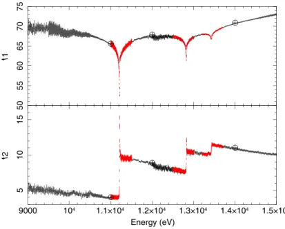
Figure14shows the derivedf1andf2near the iridium L-edges to clarify the iridium L-edge structures. The energies of the iridium L-edges6,18are indicated with dashed lines. The peak and oscillation structures off2 near the iridium L3 and L2 edges are known as the x-ray absorption near edge structure (XANES),23and the peaks indicate the absorption threshold resonances asso- ciated with the excitation of2pelectrons to unfilleddstates in the valence band.23,24Because the
1.1×10⁴ 1.15×10⁴ 1.2×10⁴ 1.25×10⁴ 1.3×10⁴
0.90.9511.05
Ratio(0.2−0.4/0.2−0.5)
Energy (eV) f1 f2
Fig. 12 Ratio of atomic scattering factors obtained when the data obtained at 0.5 deg are included to those when they are not included.
505560657075
f1
9000 104 1.1×10⁴ 1.2×10⁴ 1.3×10⁴ 1.4×10⁴ 1.5×10⁴
51015
f2
Energy (eV)
Fig. 11 Atomic scattering factors obtained in the energy scan. The black and red data present the results obtained from the coarse and fine pitch scans, respectively. The results of the angle scan at E¼11;000, 12,000, and 14,000 eV are also plotted as open circles.
L1 edge corresponds to the excitation of the electrons from the2sstates, no peak occurs near the L1 edge. To characterize the L-edge structures, we fitted thef2obtained from the fine pitch scans with a Lorentzian + arctan model in which a Lorentzian represents a sharp line and an arctan represents a step-like edge feature.25The L-edge structures were well represented by this model as seen in Fig.14. The best values are listed in Table6. The best fit parameters of the L3 edge were consistent with those by Monteseguro et al.25The center energy of the arctan model rep- resenting a step-like edge feature is consistent with the L3 and L2 edge energies, although the best fitted center energy for iridium L1 edge is∼8 eVgreater than the iridium L1 edge energy.
Although the recommended value of the L1 edge energy was 13418.5 eV,18Bearden (1967)26 reported an L1 edge energy of 13,423 eV from his measurement. Our result was close to the measurement of Bearden (1967).
505560657075
f1
9000 104 1.1×10⁴ 1.2×10⁴ 1.3×10⁴ 1.4×10⁴ 1.5×10⁴
51015
f2
Energy (eV)
Fig. 13 The atomic scattering factorsf1andf2of iridium corrected with the ratios shown in Fig.12.
The results obtained using the fine pitch scan are plotted in red. The results from the angle scans at 11,000, 12,000, and 14,000 eV are indicated by open circles.
Fig. 14 Atomic scattering factors near the iridium L-edges. The black and red data indicate the results obtained from the coarse and fine pitch scans, respectively. The dashed lines indicate the tabulated energies of the iridium L-edges.18The solid lines present the best-fit Lorentzian + arctan model. The best-fit values are listed in Table6.
4.4 Comparison with Previous Results and Effects of Overlayer with f1 and f2
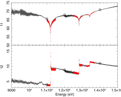
The atomic scattering factors were obtained with an energy pitch of 10 or 1.5 eV in an energy range of 9 to 15 keV based on the measurement of the reflectivity. The results were compared with the values reported by Henke et al.6As mentioned in Sec.4.2, the values obtained in this work were slightly smaller than those of Henke et al.6Figure15shows the results of the coarse pitch scan data with 0.97 times the values reported by Henke et al.6
Graessle et al.8reported the iridium optical constants for the Chandra x-ray mirrors by con- sidering the x-ray reflectance measurements at 0.05 to 12 keV. When no overlayer model was used, the angle scan data at 10 keV were represented consideringβ¼2.3106×10⁻⁶, which is 1.2% smaller than the value of2.3386×10−6 used by Henke et al.6When the overlayer model was applied, the optical constantβwas changed to 2.358×10⁻⁶, whereasδremained almost constant (δ∼3.35×10⁻⁵). Massahi et al. (in prep.) pointed out the presence of the overlayer on the SPO plates by considering the calibrations in the lower energy band. Thus, we applied the overlayer model to our angle scan data at the energies of 11, 12, and 14 keV. In the employed overlayer model, we assumed a hydrocarbon chain of the formCH2with a density of1 g∕cm3,
Table 6 Best fit parameters of L-edge structure with a Lorentzian and arctan model.
L3 edge L2 edge L1 edge
Lorentzian
Center energy (eV) 11217.90.2 12827.30.3 —
Width (eV) 6.70.4 4.60.8 —
Integrated intensitya 20.41.0 8.00.8 —
Arctan
Center energy (eV) 11215.70.3 12824.30.9 13426.50.6
χ2∕d:o:f 36.0/59 20.6/59 28.5/62
Error ranges represent1σconfidence boundaries for a parameter of interest (χ2minþ1).
aThe best fit integrated intensities forf2obtained with the overlayer model are21.91.0for L3 edge and8.4 0.9for L2 edge.
5055606570
f1
9000 104 1.1×10⁴ 1.2×10⁴ 1.3×10⁴ 1.4×10⁴ 1.5×10⁴
51015
f2
Energy (eV)
Fig. 15 Derived scattering factors as a function of energy (black) compared to Henke et al.’s values5(red dots) scaled to 97% to match the scattering factors derived in this work.
![Figure 3 shows the mean intensities of the backgrounds for each 3 s as a function of the elapsed time from 0:00 [Japan Standard Time (JST) (= UTC + 9 h)] on January 20, 2019](https://thumb-ap.123doks.com/thumbv2/123deta/6955753.2272730/6.918.317.595.706.1040/figure-intensities-backgrounds-function-elapsed-japan-standard-january.webp)