Challenge for Analog Circuit Testing in Mixed-Signal SoC
Haruo Kobayashi
Professor, Gunma University
[email protected]
Dec. 16, 2016
Contents
1. Introduction
2. Review of Analog Circuit Testing in Mixed-Signal SoC
3. Research Topics
4. Challenges & Conclusion
1. Introduction
Cost and Quality for Test Cost
● Analog portion continues to be difficult part of SoC test.
● Concept of “cost” and “quality” makes “issues and challenges of
analog circuit testing in mixed-signal SoC”
clear and logical.
● LSI testing technology
reduces cost and improves quality
simultaneously.
2. Review of Analog Circuit Testing
in Mixed-Signal SoC
Management Strategy
● Strategy 1 :
Use low cost ATE and develop analog BIST/BOST to make testing cost lower.
● Strategy 2 :
Use high-end mixed-signal ATE
as well as its associated services & know how.
Fast time-to-market & no BIST
can make profits much more than testing cost.
ATE: Automatic Test Equipment
BIST: Built-In Self-Test, BOST: Built-Out Self-Testy
Save or Earn
Low Cost Testing
Ideal : No testing
● Design guarantee
● 100% chips work well
Reality :
● Low cost ATE
● Short testing time
● Multi-site testing
● Minimum or no chip area penalty for BIST
● Extensive usage of BOST
Test and Measurement are different
● Production Test : 100% Engineering Decision of “Go” or “No Go”
For example, it can be performance comparison between DUT and “Golden Device”.
● LSI testing is manufacturing engineering.
● Measurement : 50% Science, 50% Engineering Accurate performance evaluation of circuit
Measurement can be costly, but testing should be at low cost.
DUT: Device Under Test
Analog BIST
● BIST for digital : Successful
BIST for analog : Not very successful Challenging research
● Digital test : Functionality Easy
Analog test : Functionality & Quality Hard
● In many cases
- Analog BIST depends on circuit.
- No general method like scan path in digital.
- One BIST, for one parameter testing
Analog: parametric fault as well as fatal fault.
Prof. A. Chatterjee
Specification-based Test Alternative Test Defect-based Test
RF / High-Speed IO / Power Device Testing
● RF / HSIO / Power testing is different from analog testing technology.
● These testing technologies are other challenging areas.
● RF testing items examples:
- EVM test
- System level testing, GSM/EDGE - AM/PM distortion
- Jitter, Phase noise
Robust Design and Testing
Robust design makes its testing difficult.
● Feedback suppresses
parameter variation effects.
● Self-calibration and redundancy hide defects in DUT.
● Secure DUT is difficult to test.
+
R1 R2
Robust design (yield enhancement) and testing cost reduction
are trade-off.
ATE for Mixed-Signal Testing
● Analog part is costly for development.
● Analog BIST is also beneficial
for mixed-signal ATE manufacturer
● ATE must be designed with today’s technology for tomorrow’s higher performance chip testing.
Interleaved ADC used in ATE
to realize very high sampling rate
with today’s ADCs
Low Cost ATE
● Digital ATE
- No analog option such as
Arbitrary Waveform Generator: AWG - Input/output are mainly digital.
● Replacement of analog ATE with digital ATE - Multi-site testing becomes possible.
- Still short testing time is important.
● Secondhand ATE, In-house ATE
● ATE with well balanced modular hardware
and software
Cooperation among Engineers
● Collaboration is important - Circuit designer
- LSI testing engineer
- ATE manufacturer engineer - Management
- LSI testing researcher in academia
● Strong background of analog circuit design as well as LSI testing are required
for analog testing research.
3. Research Topics
Collaboration with Socionext Inc.,
STARC and other related industries
Phase Noise Test with ΔΣ TDC BOST solution
TDC BOSTs for Timing Signal Testing BOST solution
[2] R. Jiang, H. Kobayashi, Y. Ozawa, R. Shiota, K. Hatayama, et. al.,
“Successive Approximation Time-to-Digital Converter with Vernier-level Resolution”,
IEEE International Mixed-Signal Testing Workshop, Catalunya, Spain (July 4-6, 2016).
On-chip Jitter Measurement Circuit BIST solution
DFT for SAR ADC Linearity BIST Solution
[4]
Low IMD3 2-Tone Signal Generation with AWG for Communication Application ADC Testing
Low Cost ATE
Multi-tone Curve Fitting Algorithm for Communication Application ADC
Algorithm
Complex Multi-Bandpass ΔΣ Modulator for I-Q Signal Generation
ATE for
Mixed-Signal
Testing
Time Interleaved ADC in ATE System ATE for Mixed-Signal
Testing
4. Challenges & Conclusion
Challenges of Analog Testing
● Use all aspects of technologies - Circuit technique
- Cooperation among BIST, BOST & ATE as well as software & network - Signal processing algorithm
- Use resources in SOC
such as μP core, memory, ADC/DAC
There is no science without measurement.
There is no production without test
No royal road to analog testing
Explicit Analysis of Channel Mismatch Effects in Time-Interleaved ADC Systems
N.Kurosawa, K.Maruyama, H.Kobayashi, H.Sugawara and K.Kobayashi y
Gunma University, Japan y Teratec Corp. Japan
発表内容
1.
研究の目的2.
インターリーブADC
の原理と問題点3.
ミスマッチが独立して存在する場合の影響4.
ミスマッチが同時に存在する場合の影響5.
帯域ミスマッチの影響6.
まとめ1. 研究の目的
研究の目的
インターリーブ・アーキテクチャを用いて 最高速の ADC を実現する場合の、
システム上の問題の理論解析を行う。
2. インターリーブ ADC の原理と問題点
高速・高精度
ADC
の構成²
高速ADC
の構成±
大部分の回路が比較的低い周波数のクロックで動作±
周波数の高い信号の発生が不要±
周波数の高い信号が不要±
タイミングの問題が少ない(
例:
タイミングスキュー)
²
高精度ADC
の構成±
高精度回路が不要±
大きなプロセス変動を許容±
低ノイズ回路・デバイスが不要 例:
デルタ・シグマADC
¦
サブミクロンCMOS
のアナログCMOS
回路!
高精度回路が不要!
低ノイズ回路が不要マルチプロセッサ構成
²
デジタルの世界では、マルチプロセッサ構成は非常に一般的±
多くの低性能プロセッサ±
高性能を実現²
問題点±
ソフトウエア開発の負担が重い±
マルチプロセッサの性能¿
プロセッサ1個のM
倍の性能M
:プロセッサ数インターリーブ
ADC
の原理と問題点² M
個のADC
のインターリーブでM
倍のサンプリングレートを実現±
マルチプロセッサ構成の観点から、非常に効果的±
サンプリングレートの高いADC
に適している²
チャネル間ミスマッチによってS/N
が低下 通常キャリブレーションが必要アナログ回路システムのミスマッチ
²
回路レベルのミスマッチ例
:
差動ペアのオフセットV os (V os ) rms / 1
p W L
²
システムレベルのミスマッチ例
:
インターリーブADC
のチャネル間のミスマッチ3. ミスマッチが独立して
存在する場合の影響
チャネル間ミスマッチの影響
- オフセットミスマッチの影響
オフセットミスマッチのモデル
オフセットミスマッチの時間領域での影響
²
パターンノイズ±
ほぼ入力周波数と独立±
加算的ノイズ± f s =M
周期f s :
サンプリング周波数M :
チャンネル数² 4
チャンネルADC
のシミュレーション±
正弦波入力ADC
システムの出力とエラーオフセットミスマッチの周波数領域での影響
²
パターンノイズの周波数± f noise = k £ f s =M k = 1; 2; 3; ¢ ¢ ¢
f s :
サンプリング周波数M :
チャンネル数² 4
チャンネルADC
のシミュレーション± 8192
点FFT
ADC
出力のパワースペクトラムオフセットミスマッチの
S/N
への影響² 4
チャンネル6
ビットADC
の シミュレーション²
オフセットミスマッチ:S/N
は入力周波数に独立ノイズレベルは入力振幅に独立
ADC
システムのS/N
チャネル間ミスマッチの影響
- ゲインミスマッチの影響
ゲインミスマッチのモデル
ゲインミスマッチの時間領域での影響
²
パターンノイズ±
入力正弦波のピークでエラー最大±
乗算的ノイズ(AM
ノイズ)
² 4
チャンネルADC
のシミュレーション±
正弦波入力ADC
システムの出力とエラーゲインミスマッチの周波数領域での影響
²
パターンノイズの周波数± f noise = f in § k £ f s =M k = 1; 2; 3; ¢ ¢ ¢
f s :
サンプリング周波数f in :
入力周波数M :
チャンネル数² 4
チャンネルADC
のシミュレーション± 8192
点FFT
ADC
出力のパワースペクトラムゲインミスマッチの
S/N
への影響² 4
チャンネル6
ビットADC
の シミュレーション²
ゲインミスマッチ:S/N
は入力周波数に独立 入力振幅に独立ADC
システムのS/N
チャネル間ミスマッチの影響
- タイミングスキューの影響
タイミングスキューのモデル
タイミングスキューの出力への影響
タイミングスキューの時間領域での影響
²
パターンノイズ±
入力正弦波のゼロ交差(
スルーレート最大)
付近で最大のエラー±
ゲインミスマッチとは逆± PM
ノイズ² 4
チャンネルADC
のシミュレーション±
正弦波入力ADC
システムの出力とエラータイミングスキューの周波数領域での影響
²
パターンノイズの周波数± f noise = f in § k £ f s =M k = 1; 2; 3; ¢ ¢ ¢
f s :
サンプリング周波数f in :
入力周波数M :
チャンネル数±
ゲインミスマッチの場合と同じ² 4
チャンネルADC
のシミュレーション± 8192
点FFT
ADC
出力のパワースペクトラムタイミングスキューの
S/N
への影響² 4
チャンネル6
ビットADC
の シミュレーション²
タイミングスキュー:S/N
は±
入力周波数が高くなると共に 低下±
入力振幅に独立ADC
システムのS/N
4. ミスマッチが同時に
存在する場合の影響
ミスマッチが同時に存在する場合の影響
- 2 チャンネル ADC
2ch ADC
に複数のミスマッチが同時に存在する場合のモデルV in (t) = A cos (2¼f in t) V out (nT s )
=
8 <
:
AG 1 cos f 2¼f in (nT s + ±t 1 ) g + os 1 (n : odd) AG 2 cos f 2¼f in (nT s + ±t 2 ) g + os 2 (n : even)
=
8 >
> <
> >
:
AG (1 ¡ ®) cos
½
2¼f in
µ
nT s ¡ ±t 2
¶¾
+ os cm ¡ os dif f (n : odd) AG (1 + ®) cos
½
2¼f in
µ
nT s + ±t 2
¶¾
+ os cm + os dif f (n : even)
(n = 0; § 1; § 2; ¢ ¢ ¢ )
2ch ADC
に複数のミスマッチが同時に存在する場合の出力V out (nT s ) = A s cos (2¼f in nT s + µ s ) +A n cos
8 <
: 2¼
0
@ ¡ f in + 1 2 f s
1
A nT s + µ n
9 =
;
+ os cm + os dif f cos
8 <
: 2¼
0
@ 1 2 f s
1
A nT s
9 =
;
A s = AG
r
cos 2 (¼f in ±t) + ® 2 sin 2 (¼f in ±t) A n = AG
r
® 2 cos 2 (¼f in ±t) + sin 2 (¼f in ±t) µ s = arctan f ® tan (¼f in ±t) g
µ n = arctan f tan (¼f in ±t) =® g
2ch ADC
に複数のミスマッチが同時に存在する場合の出力のパワースペクトラム解析式と数値計算の結果が一致 +
解析式の正当性を確認
2ch ADC
に複数のミスマッチが同時に存在する場合のSNR
の低下ミスマッチが同時に存在する場合の影響
- 4 チャンネル ADC
4ch ADC
に複数のミスマッチが同時に存在する場合のモデルV in (t) = A cos(2¼f in t) V out (nT s ) =
8 >
> >
> >
<
> >
> >
> :
AG 1 cos f 2¼f in (nT s + ±t 1 ) g + os 1 (n = 4m)
AG 2 cos f 2¼f in (nT s + ±t 2 ) g + os 2 (n = 4m + 1)
AG 3 cos f 2¼f in (nT s + ±t 3 ) g + os 3 (n = 4m + 2)
AG 4 cos f 2¼f in (nT s + ±t 4 ) g + os 4 (n = 4m + 3)
4ch ADC
に複数のミスマッチが同時に存在する場合の出力V out (nT s ) =
r
A 2 sc + A 2 ss cos
(
2¼f in nT s ¡ arctan
à A ss A sc
!)
+
r
A 2 n1c + A 2 n1s cos
8 <
: 2¼
Ã
f in + 1 4 f s
!
nT s ¡ arctan
0
@ A n1s A n1c
1 A
9 =
;
+
r
A 2 n2c + A 2 n2s cos
8 <
: 2¼
Ã
f in + 1 2 f s
!
nT s ¡ arctan
0
@ A n2s A n2c
1 A
9 =
;
+
r
A 2 n3c + A 2 n3s cos
8 <
: 2¼
Ã
f in + 3 4 f s
!
nT s ¡ arctan
0
@ A n3s A n3c
1 A
9 =
;
+ 1
4 (os 1 ¡ os 2 + os 3 ¡ os 4 ) cos
(
2¼
à 1 2 f s
!
nT s
)
+ 1 2
r
( os 1 ¡ os 3 ) 2 +( os 2 ¡ os 4 ) 2 cos
8 <
: 2¼
à 1 4 f s
!
nT s ¡ arctan
0
@ os 2 ¡ os 4 os 1 ¡ os 3
1 A 9 =
;
+ 1
4 (os 1 + os 2 + os 3 + os 4 )
4ch ADC
に複数のミスマッチが同時に存在する場合の出力のパワースペクトラム解析式と数値計算の結果が一致 +
解析式の正当性を確認
4ch ADC
に複数のミスマッチが同時に存在する場合のSNR
の低下5. 帯域ミスマッチの影響
ADC
の一次遅れ系近似H (j 2¼f ) = 1
1 + jf in =f c
ゲインj H (j 2¼f ) j = 1=
r
1 + (f in =f c ) 2
位相6 H (j 2¼f ) = ¡ arctan (f in =f c )
V in (t) = cos (2¼f in t)
のときV outk (nT s ) = G k cos (2¼f in nT s + µ k )
帯域ミスマッチの影響
- 2 チャンネル ADC
2ch ADC
に帯域のミスマッチが存在する場合のモデルV in (t) = A cos (2¼f in t) V out (nT s )
=
8 <
:
A=
q
1 + (f in =f c1 ) 2 cos f 2¼f in nT s ¡ arctan (f in =f c1 ) g (n : odd) A=
q
1 + (f in =f c2 ) 2 cos f 2¼f in nT s ¡ arctan (f in =f c2 ) g (n : even)
=
( AG 1 cos (2¼f in nT s + µ 1 ) (n : odd)
AG 2 cos (2¼f in nT s + µ 2 ) (n : even) (n = 0; § 1; § 2; ¢ ¢ ¢ )
²
帯域のミスマッチ±
ゲインと位相のミスマッチ±
ゲインミスマッチとタイミングスキューに相似±
ゲイン,
位相は周波数の関数2ch ADC
に帯域のミスマッチが存在する場合の出力V out (nT s ) = A s cos (2¼f in nT s + µ s ) +A n cos
(
2¼
Ã
¡ f in + 1 2 f s
!
nT s + µ n
)
A s = 1 2 A
r
G 2 c cos 2 (µ d ) + G 2 d sin 2 (µ d ) A n = 1
2 A
r
G 2 c sin 2 (µ d ) + G 2 d cos 2 (µ d ) µ s = arctan
8 <
:
G c sin (µ c ) cos (µ d ) + G d cos (µ c ) sin (µ d ) G c cos (µ c ) cos (µ d ) ¡ G d sin (µ c ) sin (µ d )
9 =
;
µ n = ¡ arctan
8 <
:
G c cos (µ c ) sin (µ d ) + G d sin (µ c ) cos (µ d ) G c sin (µ c ) sin (µ d ) ¡ G d cos (µ c ) cos (µ d )
9 =
;
G c = G 1 + G 2 ; G d = G 1 ¡ G 2
µ c = (µ 1 + µ 2 ) =2 ; µ d = (µ 1 ¡ µ 2 ) =2
2ch ADC
に帯域のミスマッチが存在する場合の出力のパワースペクトラム解析式と
Spice シミュレーション結果が一致 +
解析式の正当性を確認
2ch ADC
に帯域のミスマッチが存在する場合のSNR
の低下f m :
平均カットオフ周波数帯域ミスマッチの影響
- 4 チャンネル ADC
4ch ADC
に帯域のミスマッチが存在する場合のモデルV in (t) = A cos (2¼f in t) V out (nT s ) =
8 >
> >
> >
<
> >
> >
> :
G 1 cos (2¼f in nT s + µ 1 ) (n = 4m)
G 2 cos (2¼f in nT s + µ 2 ) (n = 4m + 1) G 3 cos (2¼f in nT s + µ 3 ) (n = 4m + 2) G cos (2¼f nT + µ ) (n = 4m + 3)
(m = 0; § 1; § 2; ¢ ¢ ¢ )
4ch ADC
に帯域のミスマッチが存在する場合の出力V out (nT s ) =
r
A 2 sc + A 2 ss cos
(
2¼f in nT s ¡ arctan
à A ss A sc
!)
+
r
A 2 n1c + A 2 n1s cos
8 <
: 2¼
Ã
f in + 1 4 f s
!
nT s ¡ arctan
0
@ A n1s A n1c
1 A
9 =
;
+
r
A 2 n2c + A 2 n2s cos
8 <
: 2¼
Ã
f in + 1 2 f s
!
nT s ¡ arctan
0
@ A n2s A n2c
1 A
9 =
;
+
r
A 2 n3c + A 2 n3s cos
8 <
: 2¼
Ã
f in + 3 4 f s
!
nT s ¡ arctan
0
@ A n3s A n3c
1 A
9 =
;
Asc; Ass; An1c; An1s; An2c; An2s; An3c; An3s
はf in ; f c1 ; f c2 ; f c3 ; f c4
の関数4ch ADC
に帯域のミスマッチが存在する場合の出力のパワースペクトラム解析式と
Spice シミュレーション結果が一致 +
解析式の正当性を確認
6. まとめ
研究成果
インターリーブ
ADC
のミスマッチの影響について²
複数のミスマッチが同時に存在する場合の解析式を導出²
帯域のミスマッチが存在する場合の解析式を導出²
実際のアプリケーションの80%
以上をカバーする2
チャンネルと4
チャンネルについて解析IEEE TRANSACTIONS ON CIRCUITS AND SYSTEMS—I: FUNDAMENTAL THEORY AND APPLICATIONS, VOL. 48, NO. 3, MARCH 2001 261
Explicit Analysis of Channel Mismatch Effects in Time-Interleaved ADC Systems
Naoki Kurosawa, Haruo Kobayashi, Member, IEEE, Kaoru Maruyama, Hidetake Sugawara, and Kensuke Kobayashi
Abstract—A time-interleaved A–D converter (ADC) system is an effective way to implement a high-sampling-rate ADC with relatively slow circuits. In the system, several channel ADCs operate at interleaved sampling times as if they were effectively a single ADC operating at a much higher sampling rate. However, mismatches such as offset, gain mismatches among channel ADCs as well as timing skew of the clocks distributed to them degrade S/N of the ADC system as a whole. This paper analyzes the channel mismatch effects in the time-interleaved ADC system. Previous analysis showed the effect for each mismatch individually, however in this paper we derive explicit formulas for the mismatch effects when all of offset, gain and timing mismatches exist together. We have clarified that the gain and timing mismatch effects interact with each other but the offset mismatch effect is independent from them, and this can be seen clearly in frequency domain. We also discuss the bandwidth mismatch effect. The derived formulas can be used for calibration algorithms to compensate for the channel mismatch effects.
Index Terms—A–D converter, analog circuit, calibration, channel mismatch, interleave, track/hold circuit.
I. INTRODUCTION
E
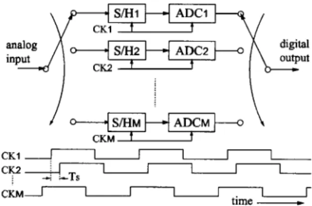
LECTRONIC devices are continuously getting faster and accordingly, the need for instruments such as digitizing oscilloscopes and large scale integrated (LSI) circuit testers to measure their performance is growing. A–D converters (ADCs) incorporated in such instruments have to operate at a very high sampling rate. This paper studies theoretical issues of a time-in- terleaved ADC system where several channel ADCs operate at interleaved sampling times as if they were effectively a single ADC operating at a much higher sampling rate [1]–[7]. Fig. 1 shows such an ADC system where each channel ADCsADC ADC ADC operates with one of phase
clocks , respectively. The sampling
rate of the ADC as a whole is times the channel sampling rate. This time-interleaved ADC system is an effective way to implement a high-sampling-rate ADC with relatively slow circuits, and is widely used. Ideally, characteristics of channel ADCs should be identical and clock skew should be zero.
However, in reality there are mismatches such as offset, gain mismatches among channel ADCs as well as timing skew of the clocks distributed to them, which cause so-called pattern noise and significantly degrade S/N (effective bits) of the
Manuscript received June 13, 2000; revised October 11, 2000. This paper was recommended by Associate Editor G. Palumbo.
N. Kurosawa, H. Kobayashi, K. Maruyama, and H. Sugawara are with the De- partment of Electronic Engineering, Gunma University, Kiryu 376-8515, Japan (e-mail: [email protected]).
K. Kobayashi is with Teratec Corporation, Tokyo 168–8501, Japan.
Fig. 1. Time-interleaved ADC system.
ADC system as a whole. Hence calibration often has to be incorporated to ensure uniformity among the characteristics of the channels. It is important to clarify the issues of the interleaved ADC architecture for designing the system. This channel mismatch in the interleaved ADC system may be called as system level mismatch or module level mismatch, while, for example, a random offset voltage in a CMOS differential pair circuit due to device size and threshold voltage mismatches may be called as circuit level mismatch.
This paper first reviews interleaving issues, the effects of offset, gain and timing mismatches individually [4]–[11]. Then, we will derive explicit formulas for the mismatch effects when all of offset, gain and timing mismatches exist together, and show that the gain and timing mismatch effects interact each other but the offset mismatch effect is independent from them.
We also analyze the bandwidth mismatch effect. The derived formulas can be used for calibration algorithms to compensate for the channel mismatch effects. In this paper, we concentrate on two-channel and four-channel interleaved systems because they cover most of the practical applications. Eight-channel or others may be sometimes used in practical situation, and the extension of the results here to an interleaved system of other channels is also possible.
Hereafter, we will use following notations:
number of channel ADCs in the ADC system;
pattern noise frequency of the ADC output;
input frequency applied to the ADC system;
sampling frequency of the ADC system;
sampling frequency of each channel ADC.
II. INDIVIDUALCHANNELMISMATCHEFFECTS
This section reviews the effects of offset, gain and timing mis-
262 IEEE TRANSACTIONS ON CIRCUITS AND SYSTEMS—I: FUNDAMENTAL THEORY AND APPLICATIONS, VOL. 48, NO. 3, MARCH 2001
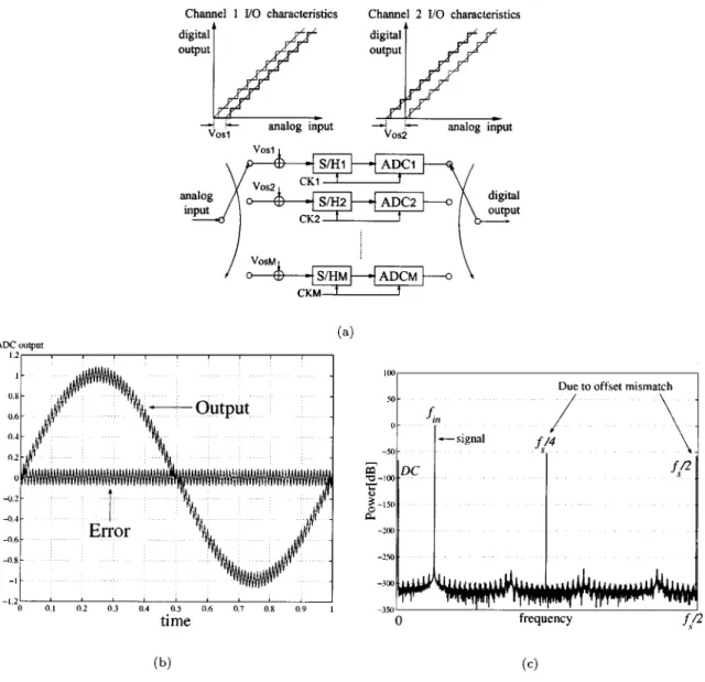
Fig. 2 Offset mismatch effect. (a) Offset mismatch model.V os represents the offset of kth channel (k = 1; 2; 1 1 1 ; M). (b) ADC output and error signals in time domain for a sinusoidal input. (c) ADC output power spectrum.
A. Offset Mismatch Effects
Suppose that the offsets of each channel are different and the other characteristics are identical (Fig. 2). This mismatch causes fixed pattern noise in the ADC system. For a dc input, each channel may produce a different output code and the period of this error signal is . The pattern noise is almost indepen- dent of the input signal in time and frequency domains, and it is additive noise in time domain while in frequency domain it causes noise peaks at
The S/N degradation of the ADC system (total pattern-noise power) due to the offset mismatch is constant regardless of the input frequency and amplitude (Fig. 3).
B. Gain Mismatch Effects
Suppose that the gains of each channel are different and the Fig. 3. Simulation results of S/N versusf of a four-channel 6-bit interleaved
KUROSAWA et al.: EXPLICIT ANALYSIS OF CHANNEL MISMATCH EFFECTS IN TIME-INTERLEAVED ADC SYSTEMS 263
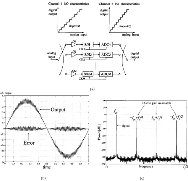
Fig. 4. Gain mismatch effect. (a) Gain mismatch model.G represents the gain of kth channel (k = 1; 2; . . . ; M). (b) ADC output and error signals in time domain for a sinusoidal input. (c) ADC output power spectrum.
signal is applied to the system, the largest difference in channel outputs occurs at the peaks of the sine wave. As with the offset mismatch case, the basic error occurs with a period of but the magnitude of the error is modulated by the input frequency . Thus, the pattern noise due to gain mismatch is multiplica- tive in time domain—which is like amplitude modulation (AM) noise—while noise spectrum peaks are at
depends on (Fig. 4) while the S/N degradation of the ADC system due to the gain mismatch is independent of (Fig. 3). Also, note that in the offset mismatch case, the S/N degradation (noise power) is independent of the amplitude of the input but in the gain mismatch case, it depends on the amplitude.
C. Clock Timing Error Effects
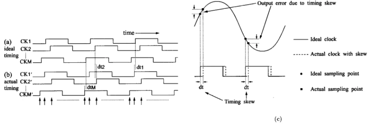
but the interleaved architecture also suffers from clock skew
effects. Suppose that the clocks have
skews (Fig. 5). This skew causes noise in the ADC system, and in the time domain the largest error oc- curs when the input signal has the largest slew rate, or crosses zero, which is like phase modulation (PM) noise (Fig. 6). The envelope of the error signal is the largest at the zero-crossings with a period of . It is shifted by 90 deg compared to the gain mismatch case. In the frequency domain, as with the gain mismatch case, the basic error occurs with a period of and the magnitude of the error is modulated by the input frequency
. The noise spectrum peaks are at
Note, that S/N degrades as increases (Fig. 3).
Remark: In offset and gain mismatch cases, the signal power at the output keeps constant as increases. On the other hand,
264 IEEE TRANSACTIONS ON CIRCUITS AND SYSTEMS—I: FUNDAMENTAL THEORY AND APPLICATIONS, VOL. 48, NO. 3, MARCH 2001
Fig. 5. Clock skew: (a) Ideal clock timing. (b) Clock timing with skews ofdt ; dt ; . . . ; dt . (c) Timing skew causes error for the sampled data.
Fig. 6. Timing skew effect. (a) Timing skew model.dt represents the skew of kth clock (k = 1; 2; . . . ; M). (b) ADC output and error signals in time domain for a sinusoidal input. (c) ADC output power spectrum.
III. COMBINEDCHANNELMISMATCHEFFECTS
In this section, we will derive explicit formulas for the mis- match effects when all of offset, gain and timing mismatches exist together, and show that the gain and timing mismatch ef- fects interact each other but the offset mismatch effect is inde-
A. Two-channel Interleaved ADC
First, we consider a two-channel interleaved ADC system.
Fig. 7 shows its configuration where each of two-channel ADCs (ADC , ADC ) operates with one of two-phase clocks ( , with a period of ), respectively. The sampling rate ( , where
) of the ADC as a whole is twice the channel sampling
KUROSAWA et al.: EXPLICIT ANALYSIS OF CHANNEL MISMATCH EFFECTS IN TIME-INTERLEAVED ADC SYSTEMS 265
Fig. 7. Two-channel time-interleaved ADC system.
system suffers from channel mismatch effects [8], [9], [11]:
gain mismatch, offset mismatch and timing mismatch. Ideally, ADC and ADC should be identical. However, in reality, their gains and offsets may be different from each other, and also the sampling timings may deviate from and . Let the gains of ADC , ADC be , respectively, and their offsets be , respectively. Also, let the sampling timing devia- tions from for ADC and for ADC be , respec- tively. Suppose that the input to the ADC is a sinusoidal signal . Then, the output of the two-channel interleaved system is given as follows:
odd even .
(1) Let
(2) Without loss of generality, we choose the timing reference so that . Then, we obtain the following:
(3) where
Remark:
1) given by (3) has four frequency components;
the frequency of the first term in (3) is , that of the second term is , the third one is 0 (dc) and the fourth one is . In other words, the first term corresponds to signal while the second term is due to gain and timing mismatches and the third term is caused by the average offset of ADC and ADC while the fourth term
Fig. 8. Simulation result of a two-channel time-interleaved ADC system with channel mismatches which verifies the correctness of our derived equation (3).
8192-point FFT was performed withA = 1, G = 1, f =f = 997=8192, gain mismatch of = 0:03, timing mismatch of t = 2:0 2 10 , average offset ofos = 2:0 2 10 , and offset mismatch of os = 9:0 2 10 in (1) and (2).
Fig. 9. Simulation result of SNR of a two-channel interleaved ADC system with gain mismatch() and timing skew (t) based on (3).
this is a very general result. However, in previous refer- ences [5], [6], [8]–[11] each channel mismatch effect in interleaved ADC systems is discussed only individually.
3) From (3) we see that the effects of gain and timing mis- match interact each other while the offset mismatch effect is independent.
4) Numerical simulations show that (1) and (3) match ex- actly; in both cases, the power at dc is 47.959 dB, the power and phase at are 0.017 038 dB, 0.107 82 deg, those at are 23.1736 dB, 64.439 deg and those at are 54.8945 dB, 0.0 deg with the simula- tion conditions in the caption of Fig. 8, where the simu- lated power spectrum is shown.
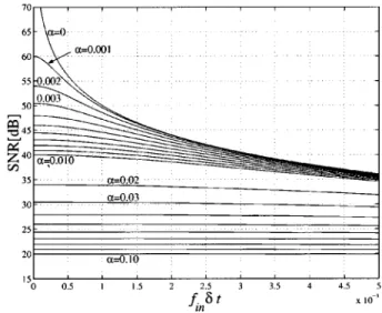
5) Fig. 9 shows numerical simulation result for the SNR due to gain mismatch and timing skew which would be useful
266 IEEE TRANSACTIONS ON CIRCUITS AND SYSTEMS—I: FUNDAMENTAL THEORY AND APPLICATIONS, VOL. 48, NO. 3, MARCH 2001
Fig. 10. Four-channel time-interleaved ADC system.
SNR of the two-channel interleaved ADC system with a parameter of gain mismatch . For example we can see in Fig. 9 that gain matching better than 0.1% is required to
obtain SNR better than 54 dB for .
Note that the offset mismatch effect is not included in Fig. 9, however, it is independent of gain and timing mis- match effects and it can be simply added to them.
Fact 1: The total power of the signal and noise at the whole system output is given by
Proof: See Appendix III.
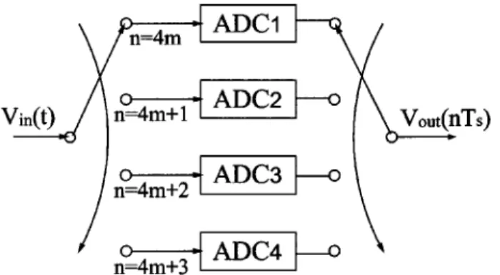
B. Four-channel Interleaved ADC
Next, we consider a four-channel interleaved ADC system, and Fig. 10 shows its configuration. Similarly, let the gains of ADC , ADC , ADC , ADC be , , , , respectively, and their offsets be , , , , respectively. Also, let the sampling timing deviations be , , , respectively.
Suppose that the input to the ADC is a sinusoidal signal
. Then, the output of the four-channel interleaved system is given as follows:
(4)
where , and let
(5) where
Without loss of generality, we choose the timing reference so that
Then, we obtain the following:
(6) where
and , , , , , , , are defined
in Appendix I.
Remark:
1) Similar arguments described in two-channel case are valid for the four-channel case.
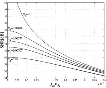
2) Numerical simulation shows that (4) and (6) match ex- actly; in both cases, the power at dc is -66.021[dB], the power and phase at are 0.041 198 [dB], 0.092 319 9 [deg], those at are 27.164 [dB], 73.792 [deg], those at are 52.041 [dB], 0.0 [deg], those at are 21.945 [dB], 80.336 [deg], those at are 28.296 [dB], 84.706 [deg] and those at are 56.478 [dB], 0.0 [deg] with the simulation conditions in the caption of Fig. 11, where the simulated power spectrum is shown.
3) Fig. 12 shows numerical simulation result for the SNR due to the gain mismatch and timing skew which would be useful for designing a four-channel interleaved system, as similar to Fig. 9 in two-channel case.
Fact 2: The total power of the signal and noise at the whole system output is given by
Proof: See Appendix III
IV. BANDWIDTHMISMATCHEFFECT
In this section, we will introduce a rather new problem, band- width mismatch, in an interleaved ADC or an interleaved sam- pling system, and then we will derive the explicit formulas for
KUROSAWA et al.: EXPLICIT ANALYSIS OF CHANNEL MISMATCH EFFECTS IN TIME-INTERLEAVED ADC SYSTEMS 267
Fig. 11. Simulation result of a four-channel time-interleaved ADC system with channel mismatches which verifies the correctness of our derived equation (6). 8192-point FFT was performed withA = 1, G = 1, f =f = 499=8192, gain mismatches of ( = 0:03, = 00:02, = 0:0 and = 00:01), timing mismatches of (t = 5:0 2 10 , t = 02:0 2 10 , t = 0:0 andt = 03:0 2 10 ), and offset mismatches of (os = 2:0 2 10 , os = 1:0 2 10 , os = 03:0 2 10 andos = 1:0 2 10 ) in eqs. (4) and (5).
Fig. 12. Simulation result of SNR of a four-channel interleaved ADC system with gain mismatch (gain deviation of = ( + + + )=4) and timing skew (timing skew deviation of = (t + t + t + t )=4) based on equation (6).
first-order system (Fig. 13). A typical example is an open-loop track/hold circuit in track mode, where the ON-resistance of the sampling switch and the hold capacitor constitute a first-order RC circuit. Here we assume that th channel ADC is approxi- mated by a first-order system and its bandwidth is given by , which can be mismatched among channels while there are no mismatches of offset, dc gain and timing discussed in the pre- vious sections. (The reader may argue that the approximation of an ADC to a first-order system might be too inaccurate, how- ever, for a track/hold circuit in track mode this approximation
Fig. 13. Bandwidth mismatch model. (a) Approximation of an ADC to the first-order system. (b) Bandwidth mismatch model in two-channel case.
each channel to one, without loss of generality, and then the fre- quency transfer function of th channel is given by
and for the input of , the output
of th channel is given by
where
(7) (8) We see that the mismatch of the bandwidth among channels
( ) causes and mismatches. Note that
and are functions of the input frequency as well as the bandwidth , and also note that when , and . Then, we will call the mismatch of as ac gain mis- match and also the mismatch of as ac phase mismatch. Re- mark that the ac gain mismatch is different from the gain mis- match discussed in Sections II and III in that ac gain mismatch depends on but the gain mismatch discussed before does not.
Also, note that the ac phase mismatch due to the bandwidth mis- match is a nonlinear function of the input frequency while the phase mismatch due to the timing skew is its linear function.
A. Two-Channel Interleaved ADC
We consider a two-channel interleaved ADC system, where the bandwidth of each channel is given by and respectively [Fig. 13(b)]. Then, when an input of
is applied, the output of the interleaved system is given by
odd
even (9) where , , and are defined in (7) and (8). Then we can obtain the following formulas:
268 IEEE TRANSACTIONS ON CIRCUITS AND SYSTEMS—I: FUNDAMENTAL THEORY AND APPLICATIONS, VOL. 48, NO. 3, MARCH 2001
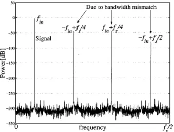
Fig. 14. Simulation result of a two-channel time-interleaved ADC system with bandwidth mismatch which verifies the correctness of our derived equation (10).
HereA = 1, f =f = 3200=(8192), f =f = 3000=(8192),f =f = 997=8192 are used, and 8192-point FFT is performed.
where
Also, SNR due to the bandwith mismatch is given by
SNR dB
Remark:
1) Numerical simulation shows that (9) and (10) match exactly; in both cases the power and phase at are
2.8844 [dB], 44.127 [deg] and that at
is 35.852 [dB], 1.7165 [deg]. with the simulation conditions in the caption of Fig. 14, where the simulated power spectrum is shown.
2) Fig. 15 shows numerical simulation result for SNR versus due to the bandwidth mismatch, which would be useful for the designer to know how much bandwidth mismatch is tolerable for a specified SNR.
Note that our simulation shows that SNR does not depend
on .
Fact 3: The total power of the signal and noise at the whole system output is given by
Fig. 15. Simulation result of SNR of a two-channel interleaved ADC system with bandwidth mismatch based on (10). Here,f = (f + f )=2 (average cut-off frequency) and = jf 0 f j=2 (cut-off frequency deviation between two channels).f =f = 997=8192 is used and 8192-point FFT is performed.
B. Four-channel Interleaved ADC
Next, we consider a four-channel interleaved ADC system, where the bandwidth of each channel is given by , and respectively. Then when the input of is applied, the output of the interleaved system is given by
(11) where
and , , , , , , and are defined in (7) and (8).
Then, we can obtain the following formulas:
(12) where
KUROSAWA et al.: EXPLICIT ANALYSIS OF CHANNEL MISMATCH EFFECTS IN TIME-INTERLEAVED ADC SYSTEMS 269
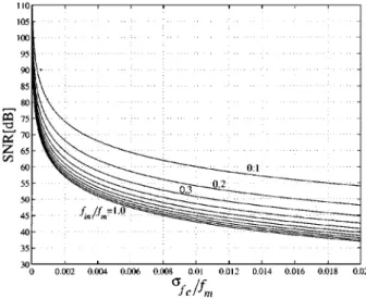
Fig. 16. Simulation result of a four-channel time-interleaved ADC system with bandwidth mismatch which verifies the correctness of our derived equation. (12). Here, A = 1, f =f = 1575=(8192), f =f = 1600=(8192), f =f = 1550=(8192), f =f = 1525=(8192), f =f = 499=8192 are used, and 8192-point FFT is performed.
Fig. 17. Simulation result of SNR of a four-channel interleaved ADC system with bandwidth mismatch based on (12). Here we consider the case that f < f < f < f and f 0 f = f 0 f = f 0 f . In the graphf = (f + f + f + f )=4 (average cut-off frequency) and = (f 0 f ) + (f 0 f ) + (f 0 f ) + (f 0 f ) )=4 (cut-off frequency deviation among four channels). 8192-point FFT is performed, andf =f = 997=8192 is used.
and and are
defined in Appendix II. The SNR is given by
SNR dB
Remark:
1) Numerical simulation shows that (11) and (12) match exactly; in both cases, the power and phase at are
3.0260 [dB], 0.004 601 13 [deg], those at are 43.980 [dB], 26.670 [deg], those at are 80.880 [dB], 0.202 41[deg] and those at
2) Fig. 17 shows numerical simulation result for SNR versus (cut-off frequency deviation among four channels)/(av- erage cut-off frequency) due to the bandwidth mismatch, which would be useful for the designer to know how much bandwidth mismatch is tolerable for a specified SNR.
Note that our simulation shows that SNR does not depend
on .
Fact 4: The total power of the signal and noise at the whole system output is given by
Proof: See Appendix III.
V. CONCLUSION
We have analyzed the channel mismatch effects in the time- interleaved ADC system, and derived explicit formulas for the mismatch effects when all of offset, gain and timing mismatches exist together. We have clarified that the gain and timing mis- match effects interact with each other but the offset mismatch effect is independent of them. Also, we discussed the band- width mismatch effect (ac mismatch effect). We have shown several graphs calculated from these formulas, which are useful for the designer to know how much mismatch is tolerable for a specified SNR. Finally, we remark that we are investigating the following as on-going projects for the time-interleaved ADC system:
• Combined channel mismatch effects for all four of offset, gain, timing and bandwidth.
• Channel linearity mismatch effects.[12]
• Algorithms to measure mismatch values and compensate for them.
APPENDIX I
This appendix gives definitions of , , , , , , , and used in Section III-B.
270 IEEE TRANSACTIONS ON CIRCUITS AND SYSTEMS—I: FUNDAMENTAL THEORY AND APPLICATIONS, VOL. 48, NO. 3, MARCH 2001
where
APPENDIX II
This appendix gives definitions of , , , , , , and used in Section IV-B.
where
APPENDIX III
This appendix gives brief proofs of Facts 1, 2, 3 and 4.
Proof of Fact 1: It follows from (3) that the total output power is given by
Proof of Fact 2: It follows from (6) that the total output power is given by
Proof of Fact 3: It follows from (10) that the total output power is given by