Comparison of Complexity of Chaos
in Many Degrees of Freedom Chaotic Circuits
Naoto Yonemoto, Katsuya Nakabai, Yoko Uwate and Yoshifumi Nishio Dept. of Electrical and Electronic Engineering, Tokushima University
2-1 Minami-Josanjima, Tokushima 770–8506, Japan Email:{yonex34, nakabai, uwate, nishio}@ee.tokushima-u.ac.jp
Abstract—This paper considers comparison of the complexity of chaos generated in many degrees of freedom chaotic circuits.
We increase the number of connected subcircuits from two to three in order to produce more complex chaos. By means of the circuit experiment and computer simulation, we show chaotic attractors. From the results, we confirmed that more complex chaos is generated in the each circuit.
I. INTRODUCTION
Chaos has two major features. They are initial value sensi- tivity and long-term unpredictability. It is difficult to predict long-term weather forecasts [1] due to initial values such as temperature, atmospheric pressure, and wind speed, etc.
Chaotic circuit is used to considers nonlinear phenomena such as natural phenomena. It is faster and easier to experiment than actual natural phenomena. Strictness analysis is difficult for chaotic phenomena generated in high-dimensional sys- tems [2]. Therefore, getting closer to high-dimensional chaos that exists in nature leads to an effect that is useful for the real world from a new perspective. For example, it may be possible to improve the confidentiality of chaotic communications [3]
or to be closer to human judgment in brain-type computers [4].
In this study, we investigate comparison of the complexity of chaos generated in many degrees of freedom chaotic circuits.
In the previous study, the circuit consists of two Inaba’s cir- cuits coupled by one linear negative resister has proposed [5].
At this time, the circuit is set a different parameter values, especially natural frequencies for each circuit. Then we com- pare the two circuits in series with the three. We show chaotic attractors generated in the circuit experiment and computer simulation.
II. SYSTEMMODEL
In the previous study, we use the circuit model of two degrees of freedom chaotic circuit in Fig. 1. This circuit was expanded from the Inaba’s circuit to two degrees of freedom chaotic circuit. In this circuit, the case where the natural frequency of the lower subcircuit was higher than the natural frequency of the upper subcircuit was investigated.
v1 i11 i12
v2 i21 i22 C1
C2
L11
L21
L12
L22 vd
vd (i12)
(i22) -g
Fig.1 Circuit model of two degrees of freedom chaotic circuit.
The parameters are described as follows:
t=√
L11C1τ,”·” =dτd,α=g
√L11
C1, β1= LL11
12,β2= LL11
21,β3= LL11
22, γ= CC1
2,ε= r1
d
√L11
C1, v1=Ex1,i11=E
√C1
L11x2,i12=E
√C1
L11x3, v2=Ex4,i21=E
√C1
L11x5,i22=E
√C1
L11x6.
The normalized circuit equations are described as follows:
˙
x1=α(x1+x4)−(x2+x3)
˙ x2=x1
˙
x3=β1(x1−f(x3))
˙
x4=αγ(x1+x4)−γ(x5+x6)
˙
x5=β2x4
˙
x6=β3(x4−f(x6)).
(1)
- 26 -
IEEE Workshop on Nonlinear Circuit Networks December 13-14, 2019
The characteristic equation for the diode is described as follows:
f(x) = 2ε1(x+ε− |x−ε|). (2) III. PROPOSED SYSTEM
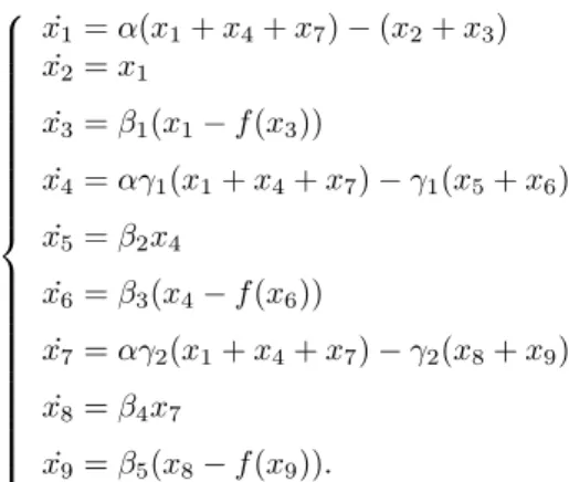
In this study, we use the circuit model of three degrees of freedom chaotic circuit in Fig. 2. This circuit consists of two degrees of freedom chaotic circuit and another Inaba’s circuit connected in series in order to produce more complex chaos.
Fig.2 Circuit model of three degrees of freedom chaotic circuit.
The parameters are described as follows:
t=√
L11C1τ,”·” = dτd,α=g
√L11
C1, β1= LL11
12,β2= LL11
21,β3= LL11
22,β4= LL11
31,β5= LL11
32, γ1= CC1
2,γ2= CC1
3,ε= r1
d
√L11
C1, v1=Ex1, i11=E
√C1
L11x2, i12=E
√C1
L11x3, v2=Ex4, i21=E
√C1
L11x5, i22=E
√C1
L11x6, v3=Ex7, i31=E
√C1
L11x8, i32=E
√C1
L11x9.
The parameters are described as follows:
˙
x1=α(x1+x4+x7)−(x2+x3)
˙ x2=x1
˙
x3=β1(x1−f(x3))
˙
x4=αγ1(x1+x4+x7)−γ1(x5+x6)
˙
x5=β2x4
˙
x6=β3(x4−f(x6))
˙
x7=αγ2(x1+x4+x7)−γ2(x8+x9)
˙
x8=β4x7
˙
x9=β5(x8−f(x9)).
(3)
The characteristic equation for the diode is described as follows:
f(x) = 2ε1(x+ε− |x−ε|). (4) IV. RESULTS
A. Two degrees of freedom chaotic circuit
We show the experimental and computer simulation results of two degrees of freedom chaotic circuit in Fig. 1. Fig. 3 (a) is the result of the top circuit from circuit experiment. Fig. 3 (b) is the result of the top circuit from computer simulation. Fig. 4 (a) is the result of the bottom circuit from circuit experiment.
Fig. 4 (b) is the result of the bottom circuit from computer simulation.
i11
v1
(a)
x
1x
2(b) Fig. 3 Chaotic attractors in the top circuit.
i21
v
2(a)
x
4x
5(b) Fig. 4 Chaotic attractors in the bottom circuit.
- 27 -
In the circuit experiment, the circuit parameters are cho- sen as C1 = 15[nF], L11 = 300[mH], L12 = 30[mH], C2 = 7.5[nF], L21 = 150[mH], and L22 = 15[mH]. In the computer simulation, the circuit parameters are chosen as α = 0.3, β1 = 10.0, β2 = 2.0, β3 = 20.0, γ = 2.0, and ε= 0.01.
As a result, the same attractors were observed qualitatively in each circuit in circuit experiment and computer simulation.
B. Three degrees of freedom chaotic circuit
In this study, we change the number of Inaba’s circuit connected from two to three. We show the experimental and computer simulation results of three degrees of freedom chaotic circuit. Fig. 5 (a) is the result of the top circuit from circuit experiment. Fig. 5 (b) is the result of the top circuit from computer simulation. Fig. 6 (a) is the result of the middle circuit from circuit experiment. Fig. 6 (b) is the result of the middle circuit from computer simulation. Fig. 7 (a) is the result of the bottom circuit from circuit experiment. Fig. 7 (b) is the result of the bottom circuit from computer simulation.
i11
v1
(a)
x
1x
2(b) Fig. 5 Chaotic attractors in the top circuit.
v2 i21
(a)
x
4x
5(b) Fig. 6 Chaotic attractors in the middle circuit.
v3 i31
(a)
x
7x
8(b) Fig. 7 Chaotic attractors in the bottom circuit.
In the circuit experiment, the circuit parameters are chosen as C1 = 15[nF], L11 = 300[mH], L12 = 30[mH], C2 = 7.5[nF], L21 = 150[mH], L22 = 15[mH], C3 = 5[nF], L31 = 100[mH], and L32 = 10[mH]. In the computer simulation, the circuit parameters are chosen as α = 0.3, β1 = 10.0, β2 = 2.0, β3 = 20.0, β4 = 3.0, β5 = 30.0, γ1= 2.0,γ2= 3.0, andε= 0.01.
Comparing the results of two degrees and three, attractors are similar in shape, and become more complex. The newly connected circuit generates more complex chaotic attractor.
V. CONCLUSION
In this study, we have investigated comparison of the complexity of chaos generated in multiple Inaba’s circuit in series. We have increased the number of connected subcircuits from two to three in order to produce more complex chaos.
We have evaluated the complexity using attractors obtained by circuit experiment and computer simulation. First, results of circuit experiment and computer simulation were qualitatively the same in the same circuit. Focusing on the chaotic attractor, more complex chaos is generated in the new connected circuit.
When we compare the same circuits, it seems that attractors become more complex.
As our future work, we will clearly evaluate the difference in complexity by using Poincare map. In addition, we will research on various network types. We will investigate interac- tions between systems [6]. We regard three degrees of freedom chaotic circuits as one system, and they will be coupled using an inductor. First, we will investigate by connecting two chaotic circuits and increasing the number of connections. At this time, we will use a network topology such as ladders, rings, and stars to investigate basic networks [7].
REFERENCES
[1] H. L. Tanaka, “Weather Forecasting and Chaos”, The Journal of Relia- bility Engineering Association of Japan 28 (7), 481-488, 2006.
[2] J. Liu, “High-Dimensional Chaotic System and its Circuit Simulation”, TELKOMNIKA, Vol. 11, No. 8, August 2013, pp. 4530 4538.
[3] X. Zhang, M. Li, Y. Hong, M. Chen, Y. Shi, L. Huang, and X. Chen,
“High-dimensional chaotic laser secure communication system based on variable laser power”, Proc. SPIE 11170, 14th National Conference on Laser Technology and Optoelectronics (LTO 2019), 111703L (17 May 2019).
[4] K. Aihara, T. Takabe, and M. Toyoda, “Chaotic neural networks”, Physics Letters A Volume 144, Issues 67, 12 March 1990, Pages 333-340.
[5] K. Suzuki, Y. Nishio, and S. Mori, “Twin Chaos - Simultaneous Os- cillation of Chaos -”, The Institute of Electronics, Information and Communication Engineers (IEICE), vol. j79-A, No. 3, pp. 813-819, Mar.
1996.
[6] S. Fujioka, Y. Yang, Y. Uwate, and Y. Nishio, “Asynchronous Oscillations of Double-Mode and N-Phase in a Ring of Simultaneous Oscillators”, 2013 International Symposium on Nonlinear Theory and its Applications NOLTA2013, Santa Fe, USA, September 8-11, 2013.
[7] K. Nakashima, K. Ueta, Y. Uwate, and Y. Nishio, “Synchronization Phenomena in Coupled Two Rings with Chaotic Circuits ”, 017 IEEE Workshop on Nonlinear Signal Processing, Feb. 10, 2017.
- 28 -