INVITED PAPER
Special Section on Leading-Edge Technology of Superconductor Large-Scale Integrated CircuitsA Reconfigurable Data-Path Accelerator Based on Single Flux Quantum Circuits
Hiroshi KATAOKA†a), Hiroaki HONDA†, Farhad MEHDIPOUR†,Nonmembers, Nobuyuki YOSHIKAWA††, Akira FUJIMAKI†††, Hiroyuki AKAIKE†††, Naofumi TAKAGI††††,andKazuaki MURAKAMI†,Members
SUMMARY The single flux quantum (SFQ) is expected to be a next- generation high-speed and low-power technology in the field of logic cir- cuits. CMOS as the dominant technology for conventional processors can- not be replaced with SFQ technology due to the difficulty of implement- ing feedback loops and conditional branches using SFQ circuits. This paper investigates the applicability of a reconfigurable data-path (RDP) accelerator based on SFQ circuits. The authors introduce detailed speci- fications of the SFQ-RDP architecture and compare its performance and power/performance ratio with those of a graphics-processing unit (GPU).
The results show at most 1600 times higher efficiency in terms of Flops/W (floating-point operations per second/Watt) for some high-performance computing application programs.
key words: single flux quantum, reconfigurable data-path, accelerator
1. Introduction
Superconducting single flux quantum (SFQ) circuit technol- ogy [1] is expected to be a next-generation circuit technol- ogy which enables ultra high-speed computation with ultra low-power consumption. The basic component of SFQ cir- cuits is a superconducting loop with Josephson junctions (JJs). A single flux quantum pulse appears as a 1 mV ex- tremely low width (in the range of pico-seconds) and car- ries information at very high speed (up to the light speed) through the circuit, while in CMOS circuits the speed is lim- ited due to the time required for charging/discharging capac- itors [1].
Further, SFQ circuits operate based on pulse logic and each gate is a clocked gate and has a function of a latch.
Hence, latches are implemented without additional costs and this makes SFQ circuits suitable for pipeline processing on streaming data. One issue in implementing very large- scale high-performance circuits by means of semiconductor circuits is the heat radiation and difficulty in high-density packaging. Unlike CMOS circuits, SFQ circuits exhibit ex- tremely low-power consumption and also very smaller area compared to the CMOS counterpart [2]. On the contrary,
Manuscript received July 16, 2013.
Manuscript revised November 1, 2013.
†The authors are with Kyushu University, Fukuoka-shi, 819- 0395 Japan.
††The author is with the Yokohama National University, Yokohama-shi, 240-8501 Japan.
†††The authors are with Nagoya University, Nagoya-shi, 464- 8601 Japan.
††††The author is with Kyoto University, Kyoto-shi, 606-8501 Japan.
a) E-mail: [email protected] DOI: 10.1587/transele.E97.C.141
SFQ circuits are not suitable for processing feedback loops and conditional branches.
Nowadays, memory wall problem is a well-known problem which comes from the gap between the operating speed of processors and that of memory. In other words, the memory bandwidth required for data transfer between general-purpose processors (GPPs) and the memory is not enough to fill this gap. In SFQ circuits, this problem might be more crucial, because implementing large-scale super- conducting random-access memory is difficult while SFQ processing units can operate so fast. Most of the accesses to memory are due to reading/writing intermediate data to/from a finite number of registers, which associates with spill code. An appropriate architecture capable of reducing the impact of spill code can alleviate the impact of memory wall problem as well.
In order to exploit the benefits of SFQ circuits in pro- viding considerably high speed and low power consumption compared to CMOS technology, a new system architecture, or SFQ-RDP system, has been introduced which consists of a CMOS GPP, a CMOS memory, and an SFQ-based re- configurable data-path (RDP) accelerator (SFQ-RDP accel- erator) [3]. Hundreds of processing elements (PEs) are ar- ranged over a two-dimensional array so that the output of each PE can be forwarded to the inputs of one or more PEs through flexible operand-routing networks (ORNs).
Since the RDP accelerator as a main component of the target architecture is implemented by SFQ circuits, obviously it can resolve most of the above-mentioned power-consumption issues originated from CMOS technol- ogy. Further, due to pipelined architecture of the RDP, the cascaded PEs can generate final results without tempo- rally memorizing intermediate data, therefore the number of load/store operations will be reduced and the memory- bandwidth pressure can be relieved. In addition, through providing the RDP with dynamic reconfiguration facility it would be possible to program processing elements and rout- ing resources at run-time. Hence, the RDP is an adaptable architecture as well.
In this paper, we provide a complete, but condensed, survey on our work on the SFQ-RDP architecture and sys- tem, most of which are reported in [4]–[6], in the project
“Low-power, High-performance, Reconfigurable Processor Using Single-Flux-Quantum Circuits” [3] in the Research Area “Technology Innovation and Integration for Informa- tion Systems with Ultra Low Power” supported by JST Copyright c2014 The Institute of Electronics, Information and Communication Engineers
RDP system as well as comparisons to graphics-processing unit (GPU) are reported. Finally, Sect. 5 concludes the pa- per.
2. Reconfigurable Data Path (RDP) Architecture As mentioned in Sect. 1, it is difficult to implement feedback loops and conditional branches using SFQ circuits. Further, any practical on-chip and off-chip SFQ memories have never been developed yet. To overcome these disadvantages, we have proposed a reconfigurable data-path (RDP) architec- ture and its application program to SFQ circuits, or SFQ- RDP [3].
Generally, RDP is a pipelined architecture comprising a two-dimensional array of processing elements (PEs) and operand-routing networks (ORNs) such that one PE can be connected through ORNs to a number of PEs in the next row.
The RDP is implemented by SFQ circuits as a substitute to CMOS circuits. Figure 1 displays the overall architecture of the proposed high-performance computer system consisting of a GPP, the RDP as accelerator, and memory elements.
Data flow graphs (DFGs) are pulled-out from critical segments of application programs, then configuration bit- streams, which are used for configuring the RDP, are gen- erated by using a dedicated tool. During execution of an application program, configurations associated with the crit-
Fig. 1 Overall architecture of the SFQ-RDP system.
a high computing throughput.
In addition to the basic properties of the RDP architec- ture, it is necessary to determine the following architectural specifications. These architectural specifications are deter- mined through the design procedure discussed in Sect. 3.1.
2.1 Input/Output Ports
I/O ports are located on top and bottom boundaries of the RDP as displayed in Fig. 1. Limitation on the number of ports depends on available memory bandwidth, RDP opera- tion frequency, width of data bus, and the number of mem- ory read/write channels.
2.2 RDP Dimensions and Layout
Figure 1 shows the height and width of RDP as the number of rows and columns, respectively.
Layout of the RDP indicates the type of functional units (FUs) and their distribution (Fig. 2). Three layout types are examined for the RDP during the design proce- dure. In a normal layout (Layout I), each FU can implement operations including addition/subtraction (ADD/SUB) and multiplication (MUL). In Layout II, every other PE imple- ments only one of the ADD/SUB and MUL operations. In the Layout III every other row of the RDP implements one of the operations. In other words, all PEs in the first row only implement MUL operations while in the second row only ADD/SUB operations are implemented.
2.3 PE Types
Three PE architectures (depicted in Fig. 3) are examined for
Fig. 2 Layout types.
Fig. 3 Various PE architectures.
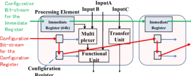
the RDP and the most suitable one is selected during the design procedure. The first PE architecture (PE I) includes an FU for implementing desired operations and a TU (trans- fer unit). As ORNs provide only routing resources between consecutive rows, TUs are utilized to connect two PEs not locating on consecutive rows. It is also possible to use an FU for implementing transfer operation. In addition, each PE has three inputs (two inputs for FU and one for TU) and two outputs (one from FU and another from TU). The second PE architecture (PE II) has one additional TU for increas- ing the flexibility of routing and it has 4-inputs/3-outputs.
The third type of PE architecture (PE III) resembles the first one, though the difference is in extending capability of im- plementing two simultaneous TUs by the FU (totally three TUs). An additional multiplexer should be used inside the PE to choose between FU’s output and the input. Each type of PE can implement various configurations depending on the states of the FU and TU (Fig. 4). Either FU or TU can be in used or unused states depending on the required func- tionality for the PE which is determined during the DFG mapping process. Also, each FU can be configured to oper- ate as a TU. For example, in PE I, it is possible to use FU and TU together (Conf. I-1), or only use the FU while the TU is unused (Conf. I-2). Further, along with utilizing the TU, FU can be either configured as unused (Conf. I-3), or can be used as a TU, which consequently provides the pos- sibility of implementing two TUs by a single PE (Conf. I-4).
Similarly, PE II, and PE III can have 6, and 5 different con- figurations, respectively.
Each FU can implement basic 64-bit double-precision floating-point operations (e.g., ADD, SUB, and MUL). Con- trol instructions (branches) and direct memory accesses via PEs are not supported. Further, 64-bit immediate regis- ters are located in each PE in order to handle immediate operands (Fig. 5).
2.4 Operand Routing Network (ORN)
PEs of each row are connected to a number of PEs in the next row through ORNs as routing resources. Figure 6 shows the definition of connection length and the maximum connection length (MCL) on a piece of RDP architecture. It can be seen that the connection length of two PEs locating in two consecutive rows is the absolute value of horizontal
Fig. 4 Various configurations for the PEs.
Fig. 5 PE’s detailed structure including immediate register and reconfiguration facilities.
Fig. 6 Definition of maximum connection length (MCL).
distance between them. (e.g., in Fig. 6, for the two PEs lo- cated on (i, j) and (i +1, j+2), the connection length is 2.)
Correspondingly, the MCL size is the maximum hor- izontal distance of two PEs located in two subsequent rows. ORNs should provide all outputs of a PE with to- tallyNi×(2×MCL+1) connections to the PEs of conse- quent row, whereNistands for the number of inputs for each PE. ORN’s functionality is similar to a multiplexer, however ORNs are composed of cross-bar switches (CBs). Similar to other components of the RDP, CBs are also implemented by means of Josephson junctions (JJs) as the basic elements of the SFQ circuits [7]. A typical ORN structure locating be- tween two rows of PEs is displayed in Fig. 7. T is the shift register which has 1-input/1-output. 2/1 CB is the cross- bar with restricted functionality for 1-output. The crossbar- based ORN has a regular pipelined structure that does not limit the performance of the RDP and can be reconfigured
Fig. 7 ORN detailed architecture (W=3 andMCL=1).
Fig. 8 The design and compilation flow for the RDP architecture.
of a PE and how it can be reconfigured during the config- uration phase. Besides programming immediate registers, multiplexers, and functional units inside PEs, ORNs should also be programmed using the configuration bits. In order to configure each component, the configuration bit-stream is serially transferred to configuration registers.
3. Design of SFQ-RDP Accelerator
3.1 Design Procedure
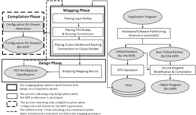
Compiler support for the RDP architecture is an essential requirement during the design procedure and hardware uti- lization phase. The extracted DFGs include a large number of operations which necessitates a sophisticated mapping tool to map DFGs onto the RDP and satisfy the architectural constraints as well. Figure 8 shows the tool chain which is similar to the conventional ones, however it has been cus- tomized for the RDP architecture [4]. The basic function- ality of this flow is to generate configuration bit-streams and an executable code for the reconfigurable accelerator.
Firstly, a hardware/software partitioning is performed on an
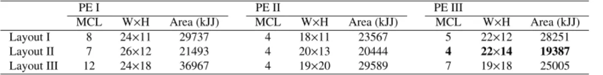
Table 1 Results of design space exploration.
PE I PE II PE III
MCL W×H Area (kJJ) MCL W×H Area (kJJ) MCL W×H Area (kJJ)
Layout I 8 24×11 29737 4 18×11 23567 5 22×12 28251
Layout II 7 26×12 21493 4 20×13 20444 4 22×14 19387
Layout III 12 24×18 36967 4 19×20 29589 7 19×18 25005
input application program. Critical segments of the program are isolated and the corresponding DFGs are generated. Due to the complexity of some attempted application programs.
(e.g., quantum chemistry application program [8]) and the necessity of careful analysis and deep knowledge on the de- tails of their implementations, the DFGs are extracted man- ually, however automatic generation is possible for some of application programs (e.g., finite difference equations [9]).
The DFGs are mapped onto the RDP through placing DFG nodes on the PE array, routing interconnections as well as assigning input/output nodes to suitable I/O ports, while considering the RDP architectural constraints. Limitations originated from the basic architecture of the RDP and from SFQ circuits (e.g., sparse routing resources, difficulties of using memory elements and register file for intermediate data, etc.) necessitate particular placement and routing al- gorithms.
Within the mapping phase, one main objective is to minimize the MCL such that the interconnections could be successfully routed. We will show that the MCL should be minimized for reducing the ORN size. Placement and rout- ing procedures ought to be iterated until a valid map satis- fying the RDP constraints are generated. A configuration bit-stream associated with each of DFGs can be generated after completion of the mapping stage. Consequently, an executable code including noncritical segments of the pro- gram code and a piece of code for RDP architecture inter- facing is generated. A part of compiler tools is customized to be utilized within the SFQ-RDP architecture design phase as shown in Fig. 8.
Determining the following essential architectural spec- ifications of the SFQ-RDP is aimed, as mentioned in Sect. 2, during the design procedure:
• the total number of required PEs in the PE array,
• suitable layout and PE architecture,
• the number of PEs in each row (width),
• the number of PE rows (height),
• the number of input/output ports,
• optimized ORN architecture with minimum number of CBs,
• the total number of ORNs, and
• the size of ORNs including the numbers of in- puts/outputs and CBs for each ORN which necessitates obtaining the MCL size as well.
During the design procedure, first all the DFGs ex- tracted from target application programs are mapped onto various RDP architectures with different layouts (depicted in Fig. 2) and PE architectures (shown in Fig. 3) (mapping phase- Fig. 8). Then the results are analyzed to decide ap-
propriate architectural specifications for the RDP (design phase- Fig. 8). In the design phase, DFGs are mapped onto the RDP without forcing any constraint except those relat- ing to the RDP basic properties, (e.g., unidirectional data flow over the PE rows, availability of routing resources only between subsequent rows, etc.), RDP layout and PE archi- tecture. The total number of RDP resources including the number of PEs and ORNs as well as ORN size, hence over- all area -in terms of the number of JJs- required for imple- menting each DFG can be calculated after mapping phase [7]. Consequently, specifications of the RDP architecture which can accommodate all the DFGs with minimum over- all area can be determined (more details in Sect. 3.2).
3.2 SFQ-RDP Design Space Exploration and Result Design of the RDP architecture entails a multitude of design parameters. Variety of design parameters indicates the high complexity of the design procedure and proves the require- ments for a methodological approach. A major challenge within the design procedure is to find a right balance be- tween the different quality requirements that a system has to meet. Design space exploration (DSE) is one approach to achieve it. DSE is the process of analyzing various imple- mentation alternatives to identify an optimal solution.
Evidences from the experiments show that aiming the MCL reduction does not necessarily result in the overall area minimization. Obviously, the RDP area is the summation of PE array’s and the ORN’s areas. The structure and area of an ORN are influenced by the RDP width, the PE structure, and the MCL size. Therefore, ORN area is differently calculated for three PE types (more details can be found in [4]).
The SFQ-RDP design space is explored for various MCL values, three PE architectures, and three layouts to ob- tain the minimum RDP area. The SFQ-RDP total area for each design point is calculated and the design point giving the minimum overall area is selected among the evaluated ones.
Consequently, final specifications of the RDP can be derived from Table 1, in which the MCL size, width, and height are recognized as 4, 22, and 14, respectively. Also, the Layout II is the most suitable one and PE architecture III can provide reasonably sufficient routing resources and routing flexibility to keep the overall area the smallest.
4. Performance Evaluation 4.1 Performance Evaluation Method
In this section, we evaluate the SFQ-RDP system which
accomplished, based on simple analytical model and simu- lation. Total execution time of a programTtotal is obtained as shown in Eq. (1).
Ttotal =Tgpp+Trd p+Toh (1)
Tgpp is the execution time obtained by executing applica- tion’s object program on SimpleScalar [10] which is a cycle- accurate processor simulator. Trd pis the execution time of the pipelined execution model which we developed in [5].
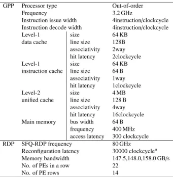
Tohis an overhead time required for driving the SFQ-RDP accelerator. Architectural parameters used for the perfor- mance evaluation are shown in Table 2.
The GPUs used for comparisons are NVIDIA Tesla M2050 and GTX280 [11]. Performance evaluation results for the GPU are borrowed from [6], [12], [13]. In addition, memory bandwidths assumed for SFQ-RDP evaluation are 148.0 GB/s, 147.5 GB/s, and 158.0 GB/s for 3D-Heat, 2D- Heat, and 2D-FDTD, respectively [11]. These values are corresponding to the memory bandwidths available in the above GPU boards.
For the estimation of the power/performance ratio, the power consumption of SFQ-RDP accelerator, GPU proces- sor, and GPU board are required. The power consumption of the SFQ-RDP accelerator is estimated as a sum of power
Table 2 Configurations of GPP and SFQ-RDP processor.
GPP Processor type Out-of-order
Frequency 3.2 GHz
Instruction issue width 4instruction/clockcycle Instruction decode width 4instruction/clockcycle
Level-1 size 64 KB
data cache line size 128B
associativity 2way hit latency 2clockcycle
Level-1 size 64 KB
instruction cache line size 64 B associativity 1way hit latency 1clockcycle
Level-2 size 4 MB
unified cache line size 128 B associativity 4way hit latency 16clockcycle Main memory bus width 64 B
frequency 400 MHz access latency 300 clockcycle
RDP SFQ-RDP frequency 80 GHz
Reconfiguration latency 30000 clockcyclea Memory bandwidth 147.5,148.0,158.0 GB/s
No. of PEs in a row 22
No. of PE rows 14
aBased on SFQ-RDP frequency (80 GHz)
the entire GTX280 board, which corresponds to∼70 W. As- suming that the memory module consumes 70 W for both M2050 and GTX280, we can conclude that the GPUs them- selves consume 155 W and 166 W, respectively.
Total power consumption of the SFQ-RDP system is estimated as the sum of the power consumed by memory, SFQ-RDP accelerator, and cryocooler which is a specific cooling system for the SFQ circuits. We assume that the power consumption of memory for SFQ-RDP accelerator and GPU are the same, and the cryocooler consumes 1000 times higher than that of the SFQ-RDP accelerator [16].
4.2 Performance Evaluation Results
The performance of 3D/2D-Heat and 2D-FDTD applica- tion programs on SFQ-RDP system and GPU are shown in Fig. 9. For 3D-Heat, 2D-Heat, and 2D-FDTD, the SFQ- RDP system is almost 18%, 20% and 25% less, respectively compared with the GPU. Although the performance of the SFQ-RDP system is lower than that of GPU, it is almost comparable to GPU.
The power/performance ratio results are shown in Ta- ble 3. In terms of the power/performance ratios, SFQ-RDP
Fig. 9 Performance comparisons.
Table 3 Power/performance ratio comparisons.
Application program Processor1 Board+Cryocooler2
SFQ-RDP GPU SFQ-RDP GPU
3D-Heat 430 0.27 0.23 0.19
2D-Heat 628 0.40 0.33 0.27
2D-FDTD 290 0.20 0.15 0.13
1Estimated with the power consumption of processor chip
2Estimated with power consumption of processor chip, memory, and cry- ocooler
outperforms GPU by 1600, 1600, and 1500 times for 3D- Heat, 2D-Heat, and 2D-FDTD, respectively. Therefore, the power/performance ratio of SFQ-RDP accelerator is ex- traordinarily higher than that of GPU. However, when the impact of power consumption of CMOS memory and cry- ocooler components is taken into account, advantage of the power/performance ratio decreases to around 1.2.
Current results show that SFQ-RDP system can be used as an efficient accelerator for FDM application programs in terms of power/performance ratio, which is important metric in high-performance computing systems. However, it is nec- essary to decrease total power consumption of cryocooler and memory by developing more efficient cryocooler and practical SFQ memory devices for practical usage.
5. Conclusions
We introduced a high-performance computing system, or SFQ-RDP system, which comprises a CMOS GPP, a CMOS memory, and an SFQ-RDP accelerator. We discussed the design procedure of SFQ-RDP accelerators, through which various PE architectures and layouts were examined and an optimized RDP architecture with minimum area in terms of the number of Josephson junctions was obtained.
To demonstrate the effectiveness of the SFQ-RDP sys- tem, it was compared with GPU using three finite dif- ference method programs, in terms of performance and power/performance ratio. We obtained maximally 1600 times higher efficiency for 3D-Heat application program with respect to power/performance ratio. This ratio de- creases to 1.2 when the power consumption of memory and cryocooler components is taken into account. Therefore, in terms of power/performance ratio, it is concluded that the SFQ-RDP accelerator can be used for practical scientific calculations especially for those based on finite difference methods. However, to achieve higher efficiency, decreas- ing total power consumption by developing practical SFQ memory and low-power cryocooler is inevitable.
Acknowledgement
This research was supported in part by the Research Area
“Technology Innovation and Integration for Information Systems with Ultra Low Power” of JST (Japan Science and Technology Corporation)’s CREST Program (FY 2006–
2012).
References
[1] K. Likharev and V. Semonov, “RSFQ logic/memory family: A new Josephson junction technology for sub-terahertz-clock-frequency digital systems,” IEEE Trans. Appl. Supercond., vol.1, no.1, pp.3–
28, March 1991.
[2] O.A. Mukhanov, “Energy-efficient single flux quantum technology,”
IEEE Trans. Appl. Supercond., vol.21, pp.760–769, 2011.
[3] N. Takagi, K. Murakami, A. Fujimaki, N. Yoshikawa, K. Inoue, and H. Honda, “Proposal of a desk-side supercomputer with reconfig- urable data-paths using rapid single flux quantum circuits,” IEICE Trans. Electron., vol.E91-C, no.3, pp.350–355, March 2008.
[4] F. Mehdipour, H. Honda, K. Inoue, H. Kataoka, and K. Murakami,
“A design scheme for a reconfigurable accelerator implemented by single-flux quantum circuits,” J. Systems Architecture - Embedded Systems Design, vol.57, no.1, pp.169–179, Jan. 2011.
[5] H. Honda, F. Mehdipour, H. Kataoka, K. Inoue, and K. Murakami,
“Performance evaluations of finite difference applications realized on a single flux quantum circuits-based reconfigurable accelerator,”
Asia-Pacific Signal and Information Processing Association Annual Summit and Conference 2011 (APSIPA ASC 2011), Xi’an, China, Oct. 2011.
[6] H. Honda, F. Mehdipour, H. Kataoka, K. Inoue, N. Yoshikawa, A.
Fujimaki, H. Akaike, N. Takagi, and K. Murakami, “Enhancing per- formance and power efficiencies of scientific computing through an SFQ reconfigurable data-path processor,” 5th Superconducting SFQ VLSI Workshop 2012 (SSV2012), Nagoya, Japan, Dec. 2012.
[7] I. Kataeva, A. Fujimaki, N. Yoshikawa, N. Takagi, K. Inoue, H.
Honda, and K. Murakami, “An operand routing network for an SFQ reconfigurable data-paths processor,” IEEE Trans. Appl. Su- percond., vol.19, no.3, pp.665–669, June 2009.
[8] S. Obara and A. Saika, “Efficient recursive computation of molec- ular integrals over cartesian Gaussian functions,” J. Chem. Phys., vol.84, no.7, pp.3963–3974, April 1986.
[9] W.H. Press, B.P. Flannery, S.A. Teukolsky, and T.W. Vetterling, Nu- merical Recipes in C, Cambridge University Press, 1988.
[10] T. Austin, E. Larson, and D. Ernst, “SimpleScalar: An infrastructure for computer system modeling,” Computer, vol.35, no.2, pp.59–67, Feb. 2002.
[11] NVIDIA, “Tesla M2050 and Tesla M2070/M2070Q Dual-slot Com- puting Processor Modules,” http://www.nvidia.com/docs/IO/43395/ BD-05238-001 v03.pdf, Aug. 6. 2010.
[12] T. Aoki and A. Nukada, CUDA programming primer (Japanese), Kougakusya, Tokyo, 2009.
[13] N. Takada, T. Shimobaba, N. Masuda, and T. Ito, “Speeding up of FDTD finite difference calculations by efficient use of GPU and shared memory,” (Japanese), Proc. Forum of Information Science and Technology, no.8, pp.457–462, Aug. 2009.
[14] Y. Shimamura, Y. Yamanashi, N. Yoshikawa, A. Fujimaki, N.
Takagi, and K. Takagi, “Design and implementation of SFQ floating- point multiplier and adder using 10 kA/cm2 Nb process,” Super- conductivity Centennial Conference, Den Haag, Netherlands, Sept.
2011.
[15] S. Hong and H. Kim, “An integrated GPU power and performance model,” Proc. 37th annual international symposium on Computer architecture, pp.280–289, Saint-Malo, France, June 2010.
[16] H. Ogihara, ed., Survey of Cryogenic Engineering (Japanese), Tokyo Denki University, Tokyo, 1999.
Hiroshi Kataoka received the B.E. and M.E. degrees in engineering from Kyushu Uni- versity, Japan in 2008 and 2010, respectively.
Currently, he is a researcher of Research Insti- tute for Information Technology in Kyushu Uni- versity. He is the member of IPSJ (Information Processing Society of Japan).
Farhad Mehdipour received the B.Sc. de- gree from Sharif University of Technology in 1996, and the M.Sc. and Ph.D. degrees in Com- puter Systems Architectures from the Amirkabir University of Technology in 1999 and 2006, re- spectively. He was a visiting researcher at Sys- tem LSI Lab, Kyushu University during Novem- ber 2005 to June 2006. He joined the School of Information Science and Electrical Engineer- ing at the Kyushu University as a researcher in December 2006. Since August 2010, he has been an Associate Professor in E-JUST Center at Kyushu University.
Dr. Farhad Mehdipour is a member of IEEE and his research interests include electronic design automation, high-performance and low-power micro-architectures, and cyber-physical systems.
Nobuyuki Yoshikawa received the B.E., M.E., and Ph.D. degrees in electrical and com- puter engineering from Yokohama National University, Japan, in 1984, 1986, and 1989, re- spectively. Since 1989, he has been with the De- partment of Electrical and Computer Engineer- ing, Yokohama National University, where he is currently a Professor. His research interests in- clude superconductive devices and their appli- cation in digital and analog circuits. He is also interested in single-electron-tunneling devices, quantum computing devices and cryo-CMOS devices. Prof. Yoshikawa is a member of the Institute of Electronics, Information and Communication Engineers of Japan, the Japan Society of Applied Physics, the Institute of Electrical Engineering of Japan, and the Institute of Electrical and Elec- tronics Engineers.
Akira Fujimaki received the B.E., M.E., and Dr. Eng. degrees from Tohoku University, Sendai, Japan, in 1982, 1984, and 1987, respec- tively. He was a Visiting Assistant Research Engineer at the University of California, Berke- ley, in 1987. Since 1988, he has been work- ing on superconductor devices and circuits at the School of Engineering, Nagoya University, Nagoya, Japan, where he is currently a pro- fessor. His current research interests include single-flux-quantum circuits and their applica- tions based on low- and high-temperature superconductors.
of the Japan Society of Applied Physics.
Naofumi Takagi received the B.E., M.E., and Ph.D. degrees in information science from Kyoto University, Kyoto, Japan, in 1981, 1983, and 1988, respectively. He joined Kyoto Univer- sity as an instructor in 1984 and was promoted to an associate professor in 1991. He moved to Nagoya University, Nagoya, Japan, in 1994, and promoted to a professor in 1998. He returned to Kyoto University in 2010. His current inter- ests include computer arithmetic, hardware al- gorithms, and logic design. He received Japan IBM Science Award and Sakai Memorial Award of the Information Pro- cessing Society of Japan in 1995, and The Commendation for Science and Technology by the Minister of Education, Culture, Sports, Science and Technology of Japan in 2005.
Kazuaki Murakami received the B.E., M.E., and Ph.D. degrees in computer science and engineering from Kyoto University, Japan in 1982, 1984, and 1994, respectively. From 1984 to 1987, he worked for the Fujitsu Lim- ited, where he was a Computer Architect of the mainframe computers. In 1987, he joined the Department of Information Systems of Kyushu University, Japan. He is currently a Professor of the Department of Advanced Information Tech- nology, and also the Vice President of the Insti- tute of Systems, Information Technologies and Nanotechnologies (ISIT).
He is a fellow of the IPSJ, and a member of the ACM, the IEEE, the IEEE Computer Society, the IEICE, and the JSIAM. His research interests in- clude computer system architectures, high-performance computing (HPC), embedded technologies, cyber-physical systems (CPS), and so on.