JAIST Repository
https://dspace.jaist.ac.jp/
Title ナローギャップ・ワイドギャップⅢ‑Ⅴ族化合物半導体
デバイスにおける低周波雑音
Author(s) Le, Phuong Son Citation
Issue Date 2014‑09
Type Thesis or Dissertation Text version ETD
URL http://hdl.handle.net/10119/12304 Rights
Description Supervisor:鈴木 寿一, マテリアルサイエンス研究科
, 博士
Low-frequency noise in narrow- and wide-gap III-V compound semiconductor devices
Suzuki Laboratory s1140211 LE Phuong Son
1 Introduction
III-V compound semiconductors, which have many advantages over silicon, are important materials for electronic and optical devices. For example, InAs, which has a narrow energy gapEg and a very high electron mobility µ, is a potential material for high-speed device applications. In contrast to InAs, GaN, which has a wide Eg and a moderateµ, is a promising material for high-power device applications. Although III-V compound semiconductor devices have been studied for a long time [1–3], their low-frequency noise (LFN) characterization still remains many issues.
In this work, we fabricated two-terminal (2T) devices from InAs films obtained by separation-bonding method on low-k flexible substrates (FS) (InAs/FS) [4, 5] or by direct growth on GaAs(001) (InAs/GaAs). In addition, from Al0.27Ga0.73N/GaN heterostructures, we fabricated GaN devices, ungated 2T devices as well as heterojunction field-effect transistors (HFETs), with Schottky structures and metal-insulator-semiconductor (MIS) structures in which an AlN insulator was sputtering-deposited on the AlGaN [6, 7]. Before the AlN deposition, two types of the AlGaN surface treatment were used with and without a cleaning by Semicoclean (an ammonium-based solution, ABS). Using these devices, LFN in InAs and GaN devices were investigated by using a measurement system with configurations shown in Fig. 1(a) for 2T devices and (b) for HFETs.
Figure 1: Low-frequency noise measurement system for (a) 2T devices and (b) HFETs.
2 Low-frequency noise in InAs films bonded on low-k flexible sub- strates or grown on GaAs(001)
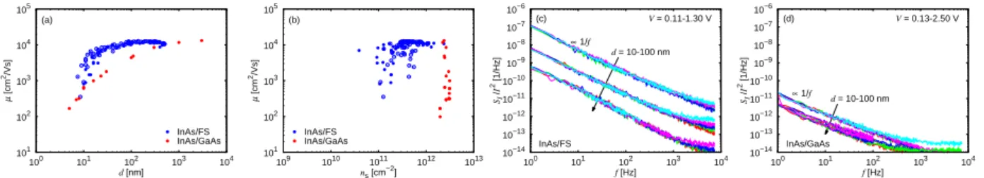
Figures 2(a) and (b) show the mobilityµas functions of the InAs thicknessdand the sheet electron concentration ns, respectively. The LFN in InAs devices shown in Figs. 2(c) and (d) exhibits that the current noise power spectrum densitySI satisfiesSI/I2'K/f with currentI and frequencyf, whereK is a constant.
101 102 103 104 105
100 101 102 103 104
µ [cm2/Vs]
d [nm]
(a)
InAs/FS InAs/GaAs
101 102 103 104 105
109 1010 1011 1012 1013
µ [cm2/Vs]
ns [cm−2] (b)
InAs/FS InAs/GaAs
10−14 10−13 10−12 10−11 10−10 10−9 10−8 10−7 10−6
100 101 102 103 104
SI /I
1 2 [1/Hz]
f [Hz]
d = 10-100 nm
InAs/FS
(c) V = 0.11-1.30 V
∝ 1/f
10−14 10−13 10−12 10−11 10−10 10−9 10−8 10−7 10−6
100 101 102 103 104
SI /I
1 2 [1/Hz]
f [Hz]
d = 10-100 nm
InAs/GaAs
(d) V = 0.13-2.50 V
∝ 1/f
Figure 2: The mobilityµas functions of (a) the InAs thicknessdand (b) the sheet electron concentrationns. SI/I2 as functions off for (c) InAs/FS and (d) InAs/GaAs withd'10, 30, 100 nm.
Figures 3(a) and (b) show SIf as functions of I to determineK. Since the device resistance is the sum of the contact resistance Rc =rc/W and the InAs channel resistance Rch =rsL/W with the contact resistivity rc, the sheet resistancers, the channel lengthL, and the device widthW, the factorK is given by
KW =(KcW/2) + (α/ns)(rs/2rc)2L
[1 + (rs/2rc)L]2 , (1)
whereKc is the factor for one contact,αandns are the Hooge parameter and the sheet electron concentration of the InAs channel, respectively. Figures 3(c) and (d) show KW as functions of L with fitting lines using Eq. (1), exhibiting K ∝1/LW, which indicates a negligible contribution of the contacts. The LFN is hence dominated by the channel, and the Hooge parameter can be calculated byα=KN=KnsLW, whereN is the electron number in the InAs channel.
10−24 10−23 10−22 10−21 10−20 10−19 10−18 10−17 10−16
10−7 10−6 10−5 10−4 10−3
SIf [A2]
I [A]
InAs/FS (a)
∝ I1 2
d = 10 nm 30 nm 100 nm
10−24 10−23 10−22 10−21 10−20 10−19 10−18 10−17 10−16
10−7 10−6 10−5 10−4 10−3
SIf [A2]
I [A]
InAs/GaAs (b)
∝ I1 2
d = 10 nm 30 nm 100 nm
10-16 10-15 10-14 10-13 10-12 10-11 10-10 10-9 10-8
10-4 10-3 10-2 10-1 100
KW [cm]
L [cm]
(c)
InAs/FS InAs 11 nm 16 nm 29 nm 100 nm 246 nm 300 nm 480 nm
10-16 10-15 10-14 10-13 10-12 10-11 10-10 10-9 10-8
10-4 10-3 10-2 10-1 100
KW [cm]
L [cm]
(d)
InAs/GaAs InAs 10 nm 23 nm 30 nm 100 nm 300 nm 1000 nm 3000 nm
Figure 3: SIfas functions ofI for (a) InAs/FS and (b) InAs/GaAs. The factorKW as functions ofLfor (c) InAs/FS and (d) InAs/GaAs.
10−4 10−3 10−2 10−1 100 101 102
100 101 102 103 104
α
d [nm]
(a) InAs/FS
InAs/GaAs
10−4 10−3 10−2 10−1 100 101 102
1012 1013 1014 1015 1016 1017 1018
α
µn s [1/Vs]
(b)
∝ 1/(µns)
InAs/FS InAs/GaAs
10−4 10−3 10−2 10−1 100 101 102
108 109 1010 1011 1012 1013 1014
α
ns [cm−2] (c)
InAs/FS InAs/GaAs α ∝ 1/n
s
10−4 10−3 10−2 10−1 100 101 102
100 101 102 103 104 105 106
α
µ [cm2/Vs]
(d)
InAs/FS InAs/GaAs α ∝ 1/µ
Figure 4: Hooge parameterαin InAs films as functions of (a) the InAs thicknessd, (b) the productµns, (c) the sheet electron concentrationns, and (d) the electron mobilityµ.
Figure 4 shows α as functions of (a) d, (b) µns, (c) ns, and (d) µ. The Hooge parameter is given by α = 1
ln(fh/f`) µ(δµ)2
µ2 +(δN)2 N
, where fh and f` are the high and low limits of the 1/f behavior [8]. For InAs/FS withd&20 nm, whereµweakly changes as seen in Fig. 2(b),α∝ns−1is observed and attributed to the carrier-number fluctuation (δN)2 ∼LW DikBT, where the interface state densityDi ∼1012 cm−2eV−1 is obtained from the data, being consistent with the Coulomb-scattering mobility [5]. For InAs/FS withd.20 nm and InAs/GaAs(001), wherensweakly changes as seen in Fig. 2(b),α∝µ−1is observed, which can be related to the mobility fluctuation due to constant fluctuations in the InAs thickness.
3 Low-frequency noise in AlGaN/GaN heterostructure
Figure 5(a) shows the product of the resistanceRand the device widthW as functions of the electrode spacing L for ungated 2T GaN devices, exhibiting a significant contribution of the contacts. The LFN spectra shown in Figs. 5(b)-(d) exhibit thatSI satisfiesSI/I2'K/f, whereK is a constant depending on device size.
0 4 8 12 16 20
0 2 4 6 8 10 12 14 16 18
RW [Ω.mm]
L [µm]
(a) MIS w ABS MIS w/o ABS Schottky
10−14 10−13 10−12 10−11 10−10 10−9
100 101 102 103 104
SI /I
1 2 [1/Hz]
f [Hz]
W = 100 µm V = 0.07-0.87 V
L = 2 µm L = 16 µm
∝ 1/f (b) MIS w ABS
10−14 10−13 10−12 10−11 10−10 10−9
100 101 102 103 104
SI /I
1 2 [1/Hz]
f [Hz]
W = 100 µm V = 0.07-0.80 V
L = 2 µm L = 16 µm
∝ 1/f (c) MIS w/o ABS
10−14 10−13 10−12 10−11 10−10 10−9
100 101 102 103 104
SI /I
1 2 [1/Hz]
f [Hz]
W = 100 µm V = 0.06-0.65 V
L = 2 µm L = 16 µm
∝ 1/f (d) Schottky
Figure 5: (a) The product of the resistanceR and the device widthW as functions of the electrode spacingL. SI/I2 as functions off for GaN ungated 2T devices, (b) MIS w ABS, (c) MIS w/o ABS, and (d) Schottky devices.
Figures 6(a)-(c) show SIf as functions of I to determine K shown in Fig. 6(d). The ungated 2T GaN devices show K 'constant for small L, indicating a significant contribution of the electrode contacts. Since the device resistance is the sum of the contact resistance and the ungated-channel resistance, we also obtained Eq. (1). Fitting data by Eq. (1), we obtainedKcW '1.9×10⁻¹²cm for one contact, which is common for the MIS and Schottky devices because of the same Ohmic process, and a Hooge parameter of the ungated region
10−18 10−17 10−16 10−15 10−14
10−5 10−4 10−3 10−2 10−1
SI
1 f
1 [A2]
I1 [A]
(a) MIS w ABS W = 100 µm
∝ I1 2
L = 2-16 µm
10−18 10−17 10−16 10−15 10−14
10−5 10−4 10−3 10−2 10−1
SI
1 f
1 [A2]
I1 [A]
(b) MIS w/o ABS W = 100 µm
∝ I1 2
L = 2-16 µm
10−18 10−17 10−16 10−15 10−14
10−5 10−4 10−3 10−2 10−1
SI
1 f
1 [A2]
I1 [A]
(c) Schottky W = 100 µm
∝ I1 2
L = 2-16 µm
10-14 10-13 10-12 10-11
10-5 10-4 10-3 10-2
KW [cm]
L [cm]
(d) KcW/2
MIS w ABS MIS w/o ABS Schottky
Figure 6: SIf as functions of I for GaN ungated 2T devices, (a) MIS w ABS, (b) MIS w/o ABS, and (c) Schottky devices. (d) The factorKW as functions ofLfor GaN ungated 2T devices.
αug'2.2×10⁻⁴for the ungated 2T MIS devices with cleaning by ABS (w ABS), 4.1×10⁻⁴ for MIS devices w/o ABS, and 5.0×10⁻⁴ for Schottky devices. The smaller αug in the MIS devices can be attributed to the lower electron mobility due to additional scattering mechanisms caused by the AlN insulator deposition, where the mobility fluctuation dominatesαug according to the Hooge theory [8].
0 2 4 6 8
0 0.4 0.8 1.2 1.6 2 2.4 KextW [10-13 cm]
RextW [Ω⋅cm]
(a) MIS w ABS
MIS w/o ABS Schottky
10−10 10−9 10−8 10−7 10−6 10−5 10−4 10−3 10−2 10−1
102 103 104 105 106 107 108 109 Kint
rs [Ω/sq.]
(b) MIS-HFET w ABS
∝rs2
∝rs−2 LG = 260 nm 160 nm
10−10 10−9 10−8 10−7 10−6 10−5 10−4 10−3 10−2 10−1
102 103 104 105 106 107 108 109 Kint
rs [Ω/sq.]
∝rs2
∝rs−2 (c) MIS-HFET w/o ABS
LG = 260 nm 160 nm
10−10 10−9 10−8 10−7 10−6 10−5 10−4 10−3 10−2 10−1
102 103 104 105 106 107 108 109 Kint
rs [Ω/sq.]
∝rs
∝rs−2 (d) Schottky-HFET
LG = 260 nm 160 nm
Figure 7: (a)KextW as functions ofRextW for the ungated part of the GaN devices. The factorKintas functions of the sheet resistancersof the gated region of GaN HFETs for (b) MIS w ABS, (c) MIS w/o ABS, and (d) Schottky devices.
The channel-current-dominated LFN in the linear regime of the GaN HFETs showsSID 'KHFETID2/f with the drain currentIDand a constant factorKHFETdepending on the gate-source voltageVG. From the ungated- device characterization, LFN behavior in the intrinsic gated region was extracted for the HFETs. Since the on-resistance Ron given by the series connection of the intrinsic resistance Rint = rsLG/W with the sheet resistancersof the gated region and the gate lengthLG, and the extrinsic resistanceRextof the ungated part,
KHFET=KintRint2
Ron2 +KextRext2
Ron2, (2)
where Kint is the factor for the intrinsic noise depending on VG, and Kext is the factor for the extrinsic noise independent of VG. From the value of the Rext obtained by DC characterization, we can evaluate Kext of the ungated part using the relation given in Fig. 7(a), and consequentlyKintby Eq. (2), as shown in Figs. 7(b)-(d).
For the small rs below the middle of 103 Ω/sq. range, Kint ∝rs−2 for both the MIS- and Schottky-HFETs.
On the other hand, the MIS-HFETs for rs & 105 Ω/sq. exhibit Kint ∝ rs2, while the Schottky-HFETs for rs&104 Ω/sq. exhibitKint ∝rs. The factorKint is given by Kint=α/N =α/nsLGW, wherens is the sheet electron concentration of the gated region. We obtained ns by integration of the capacitance by measuring capacitors fabricated simultaneously with the HFETs. As a result, we obtain the Hooge parameter α as functions ofns, shown in Fig. 8 with the point ofαug for the ungated region.
10−4 10−3 10−2 10−1 100
1010 1011 1012 1013 1014
α
ns [cm−2]
∝ n s
−1
∝ ns3
∝ ns−ξ ξ 2-3˜ (a) MIS-HFET w ABS
αug LG = 260 nm 160 nm
10−4 10−3 10−2 10−1 100
1010 1011 1012 1013 1014
α
ns [cm−2]
∝n s
−1
∝n s3
∝ns−ξ ξ 2-3˜ (b) MIS-HFET w/o ABS
αug LG = 260 nm 160 nm
10−4 10−3 10−2 10−1 100
1010 1011 1012 1013 1014
α
ns [cm−2]
∝ n s−1∝ ns3 (c) Schottky-HFET
αug LG = 260 nm 160 nm
Figure 8: The Hooge parameterαas functions of the sheet electron concentrationnsof the gated region of GaN HFETs for (a) MIS w ABS, (b) MIS w/o ABS, and (c) Schottky devices. The point ofαugis for the ungated region.
For the MIS-HFETs with the small ns . 5×1011 cm−2, α ∝ ns−1, also observed for Schottky-HFETs with ns . 1012 cm−2, and is attributed to the carrier-number fluctuation due to electron traps with density
D0 ∼1011 cm−2eV−1 in the AlGaN. On the other hand, for 5×1011 cm−2 .ns.1×1012 cm−2, the MIS- HFETs showα∝ns−ξ withξ∼2-3, which is not observed for Schottky-HFETs, and tentatively attributed to the mobility fluctuation specific for the MIS-HFETs. Moreover,α∝ns3 for both MIS- and Schottky-HFETs withns&2×1012 cm−2, can be attributed to the fluctuation in the intrinsic gate voltage, which is enhanced for large gate voltage andns by the fluctuation of the voltage across the extrinsic source resistance.
4 Conclusion
LFN in narrow- and wide-gap III-V compound semiconductors were systematically investigated for InAs (narrow- gap) and GaN (wide-gap) devices. We clarified detailed behaviors of the Hooge parameter depending on the devices.
References
[1] M. Tacano, M. Ando, I. Shibasaki, S. Hashiguchi, J. Sikula, and T. Matsui, Microelectron. Reliab.40, 1921 (2000).
[2] M. E. Levinshtein, F. Pascal, S. Contreras, W. Knap, S. L. Rumyantsev, R. Gaska, J. W. Yang, and M. Shur, Appl. Phys. Lett.72, 3053 (1998).
[3] N. Pala, R. Gaska, S. Rumyantsev, M. Shur, M. A. Khan, X. Hu, G. Simin, and J. Yang, Electron. Lett.
36, 268 (2000).
[4] H. Takita, N. Hashimoto, C. T. Nguyen, M. Kudo, M. Akabori, and T. Suzuki, Appl. Phys. Lett.97, 012102 (2010).
[5] C. T. Nguyen, H.-A. Shih, M. Akabori, and T. Suzuki, Appl. Phys. Lett.100, 012102 (2012).
[6] H.-A. Shih, M. Kudo, M. Akabori, and T. Suzuki, Jpn. J. Appl. Phys.51, 02BF01 (2012).
[7] H.-A. Shih, M. Kudo, and T. Suzuki, Appl. Phys. Lett.101, 043501 (2012).
[8] F. N. Hooge, T. G. M. Kleinpenning, and L. K. J. Vandamme, Rep. Prog. Phys.44, 479 (1981).
Table of contents
Chapter 1: Introduction 1
Chapter 2: Low-frequency noise measurement system 16
Chapter 3: Low-frequency noise in InAs films on low-kflexible substrates or GaAs(001) 28 Chapter 4: Low-frequency noise in AlGaN/GaN heterostructure 45
Chapter 5: Conclusion and future perspective 88
Appendix 90
Publication 105
Bibliography 106
List of publications
1. S. P. Le, M. Akabori and T. Suzuki: “Electron mobility anisotropy in InAs/GaAs(001)”, The seventeenth International Conference on Molecular Beam Epitaxy, Nara, Japan, September 23-28 (2012).
2. S. P. Le, T. Q. Nguyen, H.-A. Shih, M. Kudo and T. Suzuki: “Low-frequency noise of intrinsic gated region in AlN/AlGaN/GaN metal-insulator-semiconductor heterojunction field-effect transistors”, International Conference on Solid State Devices and Materials, Tsukuba, Japan, September 8-11 (2014).
3. S. P. Le, T. Q. Nguyen, H.-A. Shih, M. Kudo and T. Suzuki: “Low-frequency noise in AlN/AlGaN/GaN metal-insulator-semiconductor devices: a comparison with Schottky devices”, Journal of Applied Physics 116(2014) 054510.
Keywords
III-V compound semiconductors, InAs, AlGaN/GaN, low-frequency noise, Hooge parameter.