Japan Advanced Institute of Science and Technology
JAIST Repository
https://dspace.jaist.ac.jp/
Title
Clear Spin Valve Signals in Conventional NiFe/
In_<0.75>Ga_<0.25>As-2DEG Hybrid Two-Terminal
Structures
Author(s)
Akabori, M; Suzuki, K; Yamada, S
Citation
Proceedings of the 27th International Conference
on the Physics of Semiconductors, 772: 1373-1374
Issue Date
2005-06
Type
Journal Article
Text version
publisher
URL
http://hdl.handle.net/10119/3325
Rights
Copyright 2005 American Institute of Physics.
This article may be downloaded for personal use
only. Any other use requires prior permission of
the author and the American Institute of Physics.
The following article appeared in Masashi
Akabori, Katsushige Suzuki, and Syoji Yamada, AIP
Conference Proceedings: PHYSICS OF
SEMICONDUCTORS: 27th International Conference on
the Physics of Semiconductors - ICPS-27, 772,
1373-1374, (2005) and may be found at
http://link.aip.org/link/?apc/772/1373.
Clear Spin Valve Signals in Conventional
NiFe/In
0.75
Ga
0.25
As-2DEG Hybrid Two-Terminal Structures
Masashi Akabori, Katsushige Suzuki and Syoji Yamada
Center for Nano Materials and Technology (CNMT), Japan Advanced Institute of Science and Technology (JAlST), 1-1 Asahidai, Tatsunokuchi, Ishikawa 923-1292, Japan
Abstract. We investigated the transport properties of ferromagnetic/semiconductor hybrid two-terminal structures
utilizing an In0.75Ga0.25As/In0.75Al0.25As 2DEG formed on a GaAs (001) substrate with InxAl1-xAs step-graded buffer
layers. We used NiFe as ferromagnetic electrodes for injection/detection of spin-polarized electrons, which were formed on side walls of the semiconductor mesa to contact electron channel directly. We measured spin valve properties at low temperatures, and successfully found clear spin valve signals as well as clear channel width dependence. The results with such clear dependence suggest successful spin transport in the present samples.
INTRODUCTION
Spin field effect transistors (spin-FETs) proposed by Datta and Das [1] has been paid much attentions, because their operation is based on the combination of spin filter by ferromagnetic (FM) electrodes and spin precession by spin-orbit (SO) interaction in the channel. In order to realize spin-FETs, we have studied
spin transport in original In0.75Ga0.25As
two-dimensional electron gas (2DEG) [2], and demonstrated spin injection signals from a FM in the non-local configuration [3]. However, the previous samples were affected by the local Hall effect (LHE) via fringe field of FM contacts, therefore we could not obtain spin valve signals in the conventional configuration. In this paper, we report on the fabrication of simple two-terminal samples, and demonstrate clear spin valve signals without LHE.
EXPERIMENTAL PROCEDURE
Our 2DEG structures having large SO interactionwere a metamorphic In0.75Ga0.25As/In0.75Al0.25As
modulation doped heterostructure grown by molecular beam epitaxy. Its electron concentration and mobility
at 1.6 K are NS = 5.1×10
11
cm-2 and µ = 5.4×10⁴
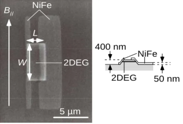
cm2/Vs, respectively. Figure 1 shows top view and
schematic cross-section of a fabricated hybrid structure. We fabricated three kind of samples with different channel width, W = 1.6 µm, 2.5µm, and 6.2 µm. The channel length, L, was fixed to 2.2 µm which is about 3.7 times as long as the estimated mean free
path le = 0.6 µm. We used electron-beam lithography
and wet etching with H2SO4-base solution for mesa
fabrication with 400-nm-depth. The FM electrodes
consisted of 50-nm-thick Ni40Fe60 were fabricated on
side walls of the mesa structures by radio-frequency sputtering process. We note that Ar-ion etching during 2 minutes in the same chamber was carried out before the formation of FM electrodes to remove native
W NiFe L 2DEG B// 5 µm 400 nm 50 nm 2DEG NiFe
FIGURE 1. Top view and schematic cross-section of a
NiFe/2DEG hybrid two-terminal structure.
1373
CP772, Physics of Semiconductors: 27th International Conference on the Physics of Semiconductors,
edited by José Menéndez and Chris G. Van de Walle
oxides on FM/2DEG contact area.
We measured transport properties by AC lock-in technique in a conventional liquid He cryostat with a super conducting magnet. Typical measurement temperature was 1.5 K.
RESULTS AND DISCUSSIONS
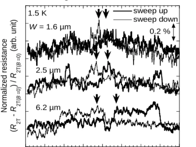
Figure 2 shows spin valve properties of the samples at 1.5K. In the present samples, symmetrical spin valve signals were clearly observed without hysterisis loops. The results suggest the present design indeed reduces the LHE. Additionally, we note that the results were obtained in longer channels with L = 2.2 µmcompared to the mean free path, le = 0.6 µm. The fact
indicates the spin relaxation should not be induced by the elastic scattering.
Furthermore, we found some unique features of spin valve peaks. Figure 3 shows the plots of peak positions and full-width half-maximum (FWHM). From the plots, as the channel width became narrower, the peak shape became sharpened and the positions were shifted close to zero field. We think such peak behaviors originate from the coercive force of FM contacts. Thus, it unfortunately depended on the aspect ratio of effective contact regions corresponding to mesa side-walls and/or excess FM parts on mesa-top. However, the results also suggest successful spin transport in the present samples due to these channel width dependence.
To confirm magnetic structures in FM contacts, we
measured magnetic force microscopy (MFM) of the hybrid structures, although the images are not shown here. We found clear domain walls at the edges of mesa-top as well as many domains in both the FM contacts on isolation area. However, we could not observe magnetic dipoles at mesa side-walls due to the limit of MFM resolution. At the present, we conclude that the deep mesa structures resulted in complex domain structures in FM contacts as well as channel width dependence of spin valve properties.
SUMMARY
We investigated spin valve properties of NiFe/
In0.75Ga0.25As-2DEG hybrid two-terminal structures
utilizing a metamorphic modulation doped heterostructure. We successfully found clear spin valve signals as well as clear channel width dependence at 1.5 K. With such clear dependence and MFM measurements, we think that the results suggest successful spin transport in the present structures.
ACKNOWLEDGEMENTS
This work is partially supported by a Grant-in-Aid for Scientific Research in Priority Areas “Semiconductor Nanospintronics” (No.14076213) of The Ministry of Education, Culture, Sports, Science and Technology, Japan, and by Mitsubishi, SCAT, and Nakajima Foundations for Science and Technology.
1. S. Datta and B. Das, Appl. Phys. Lett. 56, (l990) 665. 2. S. Gozu et al., Jpn. J. Appl. Phys. 37 (1998) L1501. 3. Y. Sato et al., Jpn. J. Appl. Phys. 40 (2001) L1093.
0 0.01 0.02 0.03 0.04 0.05 0.06 0 0.05 0.1 0.15 0 1 2 3 4 5 6 7 M a g n e tic f ie ld dif fe ren ce b e twe e n peaks ∆ B (T) Fu ll-w idth ha lf-max imu m B FW HM (T ) Channel width W (µm)
FIGURE 3. Channel width dependences of spin valve
peaks. -0.2 -0.15 -0.1 -0.05 0 0.05 0.1 0.15 0.2 No rmalize d resi s ta n ce (R 2T - R 2T (B =0 ) ) / R 2T( B =0 ) (a rb. unit )
Parallel magnetic field B
//(T) 1.5 K 0.2 % W = 1.6 µm 2.5 µm 6.2 µm sweep up sweep down
FIGURE 2. Spin valve properties of NiFe/2DEG hybrid
two-terminal structures.