Japan Advanced Institute of Science and Technology
JAIST Repository
https://dspace.jaist.ac.jp/
Title
超薄Mo1‑XNbxS2層の作製と熱電物性の研究
Author(s)
Pham, Thi Xuan
CitationIssue Date
2018‑12
Type
Thesis or Dissertation
Text versionETD
URL
http://hdl.handle.net/10119/15761
RightsDescription
Supervisor:小矢野 幹夫, マテリアルサイエンス研究
科, 博士
氏 名
Pham Xuan Thi学 位 の 種 類
学 位 記 番 号 学 位 授 与 年 月 日
博士(マテリアルサイエンス)
博材第
460号
平成
30年
12月
21日
論 文 題 目
Fabrication and Thermoelectric Properties of Ultrathin Layer of Mo1-xNbxS2論 文 審 査 委 員 主査
小矢野 幹夫 北陸先端科学技術大学院大学 教授 水田 博 同 教授 赤堀 誠志 同 准教授 ダム ヒョウ チ 同 准教授塩見 淳一郎
東京大学 教授論文の内容の要旨
Thermoelectric (TE) technology which converts waste heat directly into electrical energy using power generators, and vice versa using Peltier coolers has attracted much attention for decades. The conversion efficiency of the TE materials can be evaluated by power factor PF = S2ρ-1 and the dimensionless figure of merit ZT = (S2T)/(ρκ), where S is the Seebeck coefficient, ρ is electrical resistivity, κ denotes thermal conductivity, and T is temperature [1]. However, the intrinsically compromised behavior between S, ρ and κ causes a challenging issue for the enhancement of efficiency [2].
In the 1990s, Hicks and Dresselhaus [3] proposed the potential of low-dimensional TE materials with high ZT because of the enhancement of S caused by quantum confinement and the decrease of κ caused by the increase of surface scattering. Their idea combined with recent remarkable advances in two-dimensional (2D) materials, has spurred studies examining TE applications [4].
Among them, 2D MoS2 is the candidate for TE investigation because it has not only high power factor but also unique properties for TE devices [5], such as high mechanical flexibility and in-plane mechanical stiffness. However, the large PF of n-type MoS2 ultrathin layers obtained in the field effect transistor (FET) structure produces a complicated technique for device fabrication and creates difficulty for TE applications. Moreover, the TE properties of the p-type doped MoS2 ultrathin layers, which are fundamentally necessary for TE devices that consist of n-type and p-type TE elements [6], have not been studied.
Purpose
In this research, I investigate the TE properties of Nb-doped MoS2 ultrathin layers and the effects of Nb dopants on their TE transport properties.
Results and Discussion
The single crystals of Mo1-xNbxS2 weresynthesized by the chemical vapor transport method. The shiny property and hexagonal shape (figure 1(a)) are similar to the hexagonal crystal structure of MoS2. The smoothness and uniformity of mechanically exfoliated ultrathin layers in the atomic force microscope (AFM) image (figure 1(b)) convince the layered structure and the single crystalline of the synthesized materials.
Figure 1. (a) Optical image of a Mo0.97Nb0.03S2 flake and (b) AFM image of ultrathin
(a) (b)
The effectiveness and reliability of the fabricated devices of Nb-doped MoS2 ultrathin layers (figure 2) are supported by ohmic contacts and the temperature profile simulated via finite-element-method software Flow 3D. Figure 3(a) shows the pseudospherical constant-temperature line profile around electrodes of the sample #1. At steady state after applying 70 mW of heater power, the temperature difference in the sample T2 – T1 is 1.37 K, meanwhile, the temperature difference of the thermometers which are the junctions of Si surface (T6 – T5 = 1.24 K) and Au electrodes (T4 – T3 = 1.27 K) is 1.255 K (figure 3(b)), where T1, T2, T3, and T4 are the temperatures at the sample above electrodes 3 and 2, and at Au electrodes 5 and 6 in sequence; T5, T6, T7, and T8 are the temperatures of Si surface beneath electrodes 5, 6, 3, and 2, respectively. The small discrepancy of 1.37 and 1.255 K probably produces an error of 8% for S measurement. Thermal resistance between the sample and electrode interface at two interfaces is negligible because this effect will be cancelled by determining the temperature difference.
Figure 4 displays the ρ(T) of two ultrathin samples: #1 and #2 with the thickness of 4.5 nm and 8 nm in sequence, and a bulk sample at 300 K. The concomitant decrease in ρ with rising T indicates the semiconducting-like behavior of the two ultrathin samples. Compared with the bulk sample at 300 K, ρ of the thin samples is about one order larger. This large increase in ρ is understood by the carrier localization effect. There localized states in a tail of the valence band above the Fermi level are caused by the random potential resulting from the Nb substitution,
Figure 3. (a) Constant-temperature line profile surrounding the sample # 1.(d) Time-evolution of temperatures between the two significant points.
(b)
T6 – T5
T2 – T4 – T3 T8 – T7 (a) 28.0 ℃ 29.0 ℃ 30.0 ℃
Figure 2. Optical images of (a) sample # 1 (b) sample # 2.
Figure 4. Temperature dependence of electrical resistivities of sample # 1, sample
# 2, and bulk MoS2. The inset displays the plot of electrical conductivity σ as a
surface defects, and edge roughness. This assumption is consistent with Anderson’s prediction [7] on weak localization (WL) theory which describes the linear dependence of electrical conductivity 𝜎𝜎 with lnT as in the inset of figure 4. This result suggests that the dominant carrier conduction mechanism is WL.
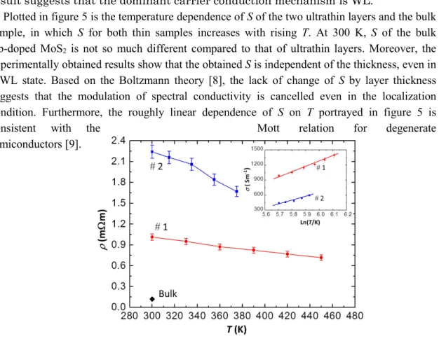
Plotted in figure 5 is the temperature dependence of S of the two ultrathin layers and the bulk sample, in which S for both thin samples increases with rising T. At 300 K, S of the bulk Nb-doped MoS2 is not so much different compared to that of ultrathin layers. Moreover, the experimentally obtained results show that the obtained S is independent of the thickness, even in a WL state. Based on the Boltzmann theory [8], the lack of change of S by layer thickness suggests that the modulation of spectral conductivity is cancelled even in the localization condition. Furthermore, the roughly linear dependence of S on T portrayed in figure 5 is
consistent with the Mott relation for degenerate
semiconductors [9].
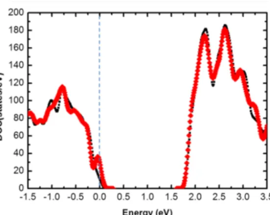
The explanation of the physical mechanism for TE transport in the MoS2 and Nb-doped MoS2 ultrathin layers is supported by first-principles calculations (figure 6). The DOS of MoS2 monolayer (black line) presents the p-type semiconducting behavior. The Fermi level is located at the top of the valence band that consists of the hybridization states of Mo 4d and S 3p orbitals. Compared to the MoS2
monolayer, the DOS for the Nb-doped MoS2 monolayer (red line) does not change.
The small DOS peak appears at the top of the valence band due to the hybridization of Nb 4d and S 3p orbitals. The Fermi level moves to the top of this DOS peak that is consistent with the experimental picture, in which the Nb-doped MoS2 electronic state is a p-type degenerate semiconductor.
Conclusion
This research investigates the TE properties of p-type Nb-doped MoS2 ultrathin layers and points out the influence of Nb dopants on TE transport properties of these ultrathin layers. This research provides an effective way to fabricate the
Figure 5. Temperature dependence of S of two thin samples, and bulk at 300 K.
Figure 6. DOS for a 6 × 6 pristine MoS2
supercell (black line) and a 6 × 6 MoS2
supercell in which one Mo atom is replaced by a Nb (red line). The vertical dashed line
devices of Nb-doped MoS2 ultrathin layers in which the Au with high work function, chemical stability, and good electrical conduction makes the good electrical contact with Nb-doped MoS2 ultrathin layers. The results of this research can be applicable to elucidate the TE transport properties in doped ultratin layers and fabricate effectively the devices of p-type doped ultrathin layers for investigating TE properties.
Keywords: MoS2, thermoelectric properties, ultrathin layer, weak localization, first-principles calculations.
論文審査の結果の要旨
遷移金属 M とカルコゲン(X=S, Se, Te)の化合物である層状遷移金属ダイカルコゲナイド MX2 は,グラフェンと同じく,機械的剥離を行う事により比較的簡単に原子層レベルの試料が 作製できるため,ポストグラフェン材料の一つとして,国内外で盛んに研究が行われている.そ の中でも二硫化モリブデンMoS2は,単層でも有限のバンドギャップを有し,高温・空気中でも 安定なため,原子層サイズのトランジスタなど次世代電子素子の基本材料として注目を集めてい る.最近では廃熱利用によるエネルギー・ハーベスティングを指向した研究も始められており,
極薄MoS2のFETを作製し,その熱電能 𝑆𝑆 と電気抵抗率 𝜌𝜌 の測定から,高いパワーファクタ ー 𝑆𝑆2⁄𝜌𝜌 が得られるという研究が報告され始めた.しかしこれらの研究では,測定された熱電 能の絶対値の不確定性や,バルクではp型伝導を示すMoS2がFET構造にするとn型になると いう矛盾を抱えるなど,解決すべき点が多いのが現状である.
本研究では,MoS2に関するこれら原子層レベルでの熱電物性に関する情報を得るため,(1) 元 素ドープによるキャリア注入を目指してMoの一部をNbで置換したMo1-xNbxS2単結晶を合成
し,(2) 熱電能を正確に計測するための素子デザインおよび素子作製行程を確立すること,さら に(3) 測定結果から,極薄層状化合物における伝導キャリア輸送に関する情報を得ることを目的 とした.
ヨウ素を輸送剤として用いた封管式化学気相法によって,置換濃度 x が 0.03 までの Mo1-xNbxS2 単結晶を合成することに成功した.さらに粘着テープを用いた機械的剥離により,
厚さが数ナノメートル,大きさがマイクロメートルオーダーの試料を自由に作製できることを確 かめた.電気抵抗率と熱電能を測定するため,剥離した試料を,シリコン基板上に形成した四端 子パターン上に移送した.この基板上には独自に設計されたマイクロヒーターと温度計も設置さ れており,電気抵抗率と熱電能を同時に測定することが可能である.試料の電圧端子間の温度差 𝛥𝛥𝛥𝛥 をシリコン基板の熱電能から測定するという独創的な手法を開発することにより,微小極薄 材料の熱電能測定が簡便かつ正確に出来るようになった.この手法の妥当性は,有限要素法によ る熱解析シミュレーションにより確かめられた.
300 Kから450 Kまでの熱電能と電気抵抗率の測定から,キャリア輸送のメカニズムについ て詳細な解析を行い,無秩序ポテンシャルによるキャリアの弱局在によって電気抵抗率が増大す ること,NbとSの混成軌道からなる準位にフェルミ準位がピンニングされていること等を新た に見出した.本研究で観測された熱電能から求めたキャリア型は p 型であり,第一原理電子状 態計算の結果とも矛盾なく合致する.
以上,本論文は,極薄Mo1-xNbxS2に対して,試料作製から素子デザインと熱電物性測定を行 い,原子層レベルの層状化合物のキャリア輸送メカニズムについて言及したものであり,学術・
応用の両面に貢献するところが大きい.よって博士(マテリアルサイエンス)の学位論文として 十分価値あるものと認めた.