Study on RF Energy Harvesting Rectenna
System from Ambient RF Signal for IoT
Applications
NGUYEN THUY LINH
Department of Computer and Network Engineering
The University of Electro-Communications
A dissertation submitted for the Degree of
Doctor of Engineering
System from Ambient RF Signal for IoT
Applications
by
NGUYEN THUY LINH
A Dissertation Submitted for the degree of
DOCTOR OF ENGINEERING
at
THE UNIVERSITY OF ELECTRO-COMMUNICATIONS
I would like to dedicate this dissertation to my dear family, especially my parents. The dissertation is my present for my father in heaven. I am thankful to my beloved husband for being together with me since married time, bringing up my two daughters - Giang and Duong, and encouraging me
during the time of this work.
First of all, I would like to emphasize my deepest appreciation to my supervi-sors, Professor Koichiro ISHIBASHI and Professor Cong-Kha PHAM, for their enthusiastic encouragement, guidance, and support during my doctor course. They have advised and taught me the way to research as a Ph.D. student. Be-sides, they inspire my interest in the development of innovative technologies. With their guidance, my knowledge is broadened.
I extremely appreciate the supports of Professor Koichiro Ishibashi to me in daily life. He always stands beside me and encourages me to overcome the hardest time in my life, especially, when my father passed away. With me, it is my pleasure to be his student. I hope that we still maintain a good relationship in the future.
I would also like to express my thanks to Doctor Yasuo Sato for his tech-nical support. He taught me to usefully utilize experimental equipment in our laboratory. Besides, he enthusiastic supports me in experiments in the real environment.
I would like to thank the University of Electro-Communications Tokyo (UEC), and JST-CREST Project, Grant Number JPMJCR16Q1, for giving me a chance to join in the Project and study in Japan. Thank them, I have an opportunity to study Ph.D. course. I also would like to send my thanks to the UEC’s professors for their guidance and support during my doctor course. I would like to send my thanks to my teachers and colleagues in the Faculty of Radio-Electronic Engineering, Le Quy Don Technical University, Ha Noi, Viet Nam. I also would like to present my thanks to all of the members of ISHIBASHI’s laboratory and my friends in Japan and in Vietnam. Their kindness encourages me to finish my course.
Last but not least, I would like to acknowledge VLSI Design and Education Center (VDEC), the University of Tokyo in collaboration with Synopsys, Inc. and Cadence Design Systems, Inc for their support for this work.
Study on RF Energy Harvesting Rectenna
System from Ambient RF Signal for IoT
Applications
APPROVED
Prof. Koichiro ISHIBASHI , Chairman
Prof. Cong-Kha PHAM
Prof. Ryo ISHIKAWA
Prof. Nobuo NAKAJIMA
Prof. Motoharu MATSUURA
by
Abstract
Study on RF Energy Harvesting Rectenna System from
Ambient RF Signal for IoT Applications
NGUYEN THUY LINH
Doctoral Program in Electronic Engineering The University of Electro-Communications
In this thesis, a structure of the RF energy harvesting (RFEH) system, which is applied for RF sensor TAG and RF sensor TAG with weak-up receiver (WuR), is studied and proposed. First, characteristics of the RF signal in the environment are analyzed; hence, essential specifications of the ambient RFEH system are pointed out. The analyzation indicates that the Q factor of RFEH system a↵ects bandwidth (BW) of the RF signal, and a wide bandwidth RFEH system is an essential structure to harvest the ambient RF signal efficiently.
Second, principle specifications a↵ecting the efficiency of a rectifier are theoretically studied and evaluated. A 3-stage cross-coupled rectifier (CCR) with the application of dynamic threshold MOSFET (DTMOS) and body-tire-to-source MOSFET (BTMOS) in 65nm Silicon on Thin Buried oxide (SOTB) technology was fabricated and evaluated. The measurement results indicate that DTMOS CCR, which has a higher drain current than that of BTMOS CCR, obtains two times output power higher than BTMOS CCR. Besides, the Q factor of the rectifier is chosen to ensure the BW of the RF signal so that the entire RF power is rectified. As a result, the output power of the rectifier when excited by modulated signals becomes two times higher than that of the rectifier when excited by a pure sine wave signal at -20 dBm input power.
alyzed in which relationships between Q factor of the total system, Q factor of the rectifier, and the Q factor of matching circuit are presented. From the methodology, the wide bandwidth RFEH system from 950 MHz cell phone RF signal is designed. In the system, the Q factor of the rectifier dominated Q factor of the total system to ensure the BW of Long-Term Evolution (LTE) signal. A wide BW matching, which is 62 MHz, between a half wavelength wired dipole antenna and the rectifier is designed to fulfill the system.
The measurement results with the 950 MHz LTE signal in the environment show that the output power of the designed system, which is 3.48 µW , is 15 times higher than that of the other study at -20 dBm input power. The designed rectenna with Yagi antenna generates 7.6 µW DC power at outdoor conditions when LTE signal is at a level of -18.6 dBm.
In conclusion, the proposed structure of the RFEH system in this work is a potential candidate for battery-less IoT applications. The designed rectenna is suitable for the RF sensor TAG and RF sensor TAG with WuR.
List of Abbreviation
BPSK Binary Phase-Shift Keying BTMOS Body-Tired-to-source MOSFET
BW BandWidth
CCR Cross-coupled rectifier
DTMOS Dynamic Threshold MOSFET DTV Digital Television
GPS Global Positioning System
ER Energy Receiver
IERC European research cluster of IoT IR Information Receiver
IoT Internet of Things LTE Long-Term Evolution MCU MicroController Unit
OFDM Orthogonal Frequency Division Multiplexing QAM Quadrature Amplitude Modulation
PAPR Peak to Average Power Ratio PCE Power Conversion Efficiency
RF Radio Frequency
RFEH RF Energy Harvesting
SWIPT Simultaneous Wireless Information and Power Transfer WIT Wireless Information Transfer
WIPT Wireless Information and Power Transmission WPBC Wirelessly Powered Backscatter Communication WPCN Wirelessly Powered Communication Network WPT Wireless Power Transfer
WSN Wireless Sensor Node WuR Wake-up Receiver
Contents
List of Figures
viiList of Tables
xii1 Introduction
11.1 Research Background
. . . 11.1.1 IoT definition and applications
. . . 11.1.2 Energy harvesting technologies
. . . 41.2 Motivation and Contributions of this study
. . . 51.2.1 Motivation
. . . 51.2.2 Research Contribution
. . . 71.3 Dissertation Layout
. . . 82 Requirements of RFEH rectenna system for IoT
applications
112.1 Characteristics of the ambient RF signal
. . . 112.1.1 The ambient RF signals in surveys
. . . 112.1.2 Characteristics of the RF signals at measurement
position of the study
. . . 122.2 Technical background
. . . 142.2.1 Energy requirement of wireless sensor node for
IoT applications
. . . 142.2.2 RFEH technique
. . . 162.2.3 Related studies on ambient RFEH
. . . 182.3.1 The proposed technique for ambient RFEH system
202.3.2 Required specifications of the proposed RFEH
system
. . . 233 Rectifier circuit
253.1 Types of rectifier circuits
. . . 253.1.1 Half-wave rectifier
. . . 253.1.2 Full-wave rectifier
. . . 273.1.3 MOSFET rectifier for RFEH system
. . . 303.2 Principle specifications a↵ect to efficiency of rectifier
. 333.2.1 Drain current
. . . 333.2.2 Q factor
. . . 383.2.3 Waveform excitation
. . . 423.2.4 Phase di↵erence
. . . 443.3 Evaluated results of fabricated rectifiers
. . . 453.3.1 Design of 3-stage DTMOS CCR and BTMOS CCR
453.3.2 Measurement results
. . . 473.3.3 Matching circuits for 3-stage CCR chip
. . . 483.3.4 Measurement results of the designed 3-stage CCR
503.4 Implement of 3-stage DTMOS CCR with floating
sub-circuit
. . . 533.4.1 Matching circuit for 3-stage CCR with floating
sub-circuits chip
. . . 533.4.2 Measurement results of 3-stage CCR with
float-ing sub-circuits
. . . 553.4.3 Measurement results of phase di↵erent e↵ect
. . . 573.5 Chapter Conclusion
. . . 594 Design of wide bandwidth RFEH rectenna to
har-vest RF energy in the ambient environment
614.1 Design methodology
. . . 61Contents
4.1.2 Antenna impedance consideration
. . . 634.2 The proposed RFEH systems from 950 MHZ cell phone
RF signals
. . . 654.3 Matching circuits and antennas
. . . 664.3.1 Matching circuit and antenna for HA RFEH rectenna
664.3.2 Matching circuit and antenna for LA RFEH rectenna
684.4 Chapter Conclusion
. . . 695 Performance of the proposed RFEH rectennas in
the ambient environment
715.1 Measurement in an Anechoic Chamber room
. . . 715.2 Indoor measurement with RF signal from ambient
en-vironment
. . . 765.2.1 RF signal in the ambient environment
. . . 765.2.2 Performance of the HA RFEH rectenna
. . . 775.2.3 Performance of the LA RFEH rectenna
. . . 805.2.4 Performance of the RFEH rectenna with CCR
circuit
. . . 815.3 Outdoor measurement with the designed dipole rectenna
. . . 845.4 Measurement with the designed Yagi rectenna
. . . 875.5 Chapter Conclusion
. . . 915.5.1 Comparison between two proposed RFEH rectenna
structures
. . . 915.5.2 Comparison results between the study and other
ambient RFEH studies
. . . 926 Conclusion and Future works
956.1 Conclusion
. . . 956.2 Applications and Future works
. . . 976.2.1 Applications of the proposed study on IoT sensors
976.2.2 Future works
. . . 97Appendix
99A Full chip photos
99B List of Publications
100B.1Journals
. . . 100B.2International Conference Presentations
. . . 100List of Figures
1.1 IoT definition by IERC [2] . . . 2
1.2 IoT applications in human social . . . 3
2.1 Measured spectrum of RF signals at the measurement place: (a) Spectrum, and (b) Magnified spectrum of the 952 MHz signal. . . 13
2.2 Map of the measurement position and picture of mobile phone antenna. . . 13
2.3 The distribution of mobile phone base station in Tokyo. . . 14
2.4 Structures of WSNs: (a) Sensor node, and (b) RF sensor TAG powered by RFEH with/without WuR. . . 15
2.5 Block diagram and equivalent circuit of RFEH rectenna: (a) Block dia-gram, and (b) Equivalent circuit . . . 16
2.6 Recent state of art in the RFEH studies . . . 18
2.7 Recent state of art in the ambient RFEH studies. . . 20
2.8 Ambient RFEH technique . . . 21
2.9 Definition of BW on the reflection coefficient to calculate Q factor of the system . . . 22
3.1 Half-wave rectifier circuits with resistive loads: (a) Half-wave rectifier, (b) Wave form of input voltage, and (c) Wave form of diode current . . . 25
3.2 Basic rectifier circuits with resistive loads: (a) Half-wave rectifier, (b) Full-wave center-tap rectifier, and (c) Full-Full-wave bridge rectifier . . . 28
3.3 Schematic of multiplier rectifiers: (a) 3-stage Cockcroft-Walton multiplier rectifier, and (b) 3-stage Dickson charge pump rectifier . . . 29
3.4 CMOS rectifier circuits: (a) Dickson charge pump rectifier, and (b) Cross-coupled rectifier CCR . . . 30
3.5 Schematic of a CCR with floating sub-circuits . . . 31
3.6 Schematic of a single stage CCR . . . 33
3.7 Simulated IV characteristic of the DTMOS diode, BTMOS diode, DTMOS CCR configuration, and DTMOS CCR with floating sub-circuits configuration 36 3.8 Simulated DC level-up amount ( V DC) from the floating sub-circuit . . . 37
3.9 Simulated the dependence of output power of the rectifier on Is0 . . . 37
3.10 Equivalent circuit of a rectifier in the RFEH rectenna . . . 38
3.11 Block diagram of N stage CCR . . . 39
3.12 Complete MOS small-signal model . . . 40
3.13 AC equivalent circuit of N stage CCR with e↵ect of parasitic components . 40 3.14 Simulated dependence of Q factor on the number of rectifier stages N-stage CCR with floating sub-circuits . . . 41
3.15 Instantaneous power of the CW signal and OFDM signal . . . 42
3.16 PAPRs of the measured RF signals with signal generator: (a) PAPR of CW signal, (b) PAPR of BPSK signal, (c) PAPR of 64 QAM signal, and PAPR of 256 QAM signal . . . 43
3.17 Dependence of DC output voltage with ' in 3-stage CCR, 3-stage CCR with floating sub-circuit using DTMOS and BTMOS. . . 44
3.18 Schematic of 3-stage CCR: (a) with BTMOS, (b) with DTMOS. . . 46
3.19 Layout of 3-stage BTMOS CCR . . . 46
3.20 Layout of 3-stage DTMOS CCR . . . 47
3.21 Evaluation setup with signal generator . . . 47
3.22 3-stage CCR with matching circuit in FR4 board . . . 48
3.23 Equivalent circuit of the rectifier and matching in the PCB board. . . 49
3.24 Measured S11 at two ports rectifier boards: (a) BTMOS CCR board, (b) DTMOS CCR board . . . 49
3.25 Measured results of 3-stage BTMOS CCR at 950 MHz: (a) Output voltage at di↵erent loads, and (b) PCE at di↵erent loads. . . 50
3.26 Measured results of 3-stage DTMOS CCR at 950 MHz: (a) Output voltage at di↵erent loads, and (b) PCE at di↵erent loads. . . 51
List of Figures
3.27 Measured output voltages of 3-stage DTMOS and BTMOS CCRs at 10
M ⌦ load: (a) Input is CW signal, and (b) Inputs are modulated signals . . 52
3.28 Measured dependence of output power of CCR on PAPR of RF signals . . 53
3.29 Matching circuit for CCR with floating sub-circuits for measurement with SG . . . 54
3.30 Measured S11 of 3-stage DTMOS CCR with floating sub-circuits: (a) at Port 1, and (b) at Port 2 . . . 55
3.31 Measured outputs of 3-stage DTMOS CCR with floating sub-circuits with CW signal: (a) Output voltage, and (b) PCE . . . 56
3.32 Measured PCE of 3-stage DTMOS CCR with floating sub-circuits: (a) at an input power of -20 dBm, and (b) at an input power of -15 dBm, . . . . 57
3.33 Evaluation conditions for phase e↵ect measurement . . . 58
3.34 Measured and simulate results of phase di↵erence e↵ect into 3-stage CCR with floating sub-circuits . . . 59
4.1 Q factor of RFEH rectenna . . . 62
4.2 Simple model of a rectenna: (a) The simple rectenna, and (b) Equivalent circuit . . . 63
4.3 Piecewise-linear model of diode forward characteristic . . . 64
4.4 Figure of the proposed HA RFEH rectenna . . . 65
4.5 Figure of the proposed LA RFEH rectenna . . . 66
4.6 Equivalent circuit of the proposed HA RFEH rectenna . . . 67
4.7 Measured impedance and S11 of the HA RFEH rectenna: (a) Impedance, (b) S11. . . 67
4.8 Equivalent circuit of the proposed LA RFEH rectenna . . . 68
4.9 Measured impedance and S11 of the LA RFEH rectenna: (a) Impedance, (b) S11. . . 69
5.1 Measure the propose RFEH rectenna in an anechoic chamber . . . 72
5.2 Measurement setup in the anechoic chamber . . . 72
5.3 Measured output of the RFEH scheme 2 when excited by CW signal: (a) Output voltage, and (b) PCE . . . 73
5.4 Measured output voltages of the proposed LA RFEH at 10 M⌦ with CW signal and modulated signal . . . 74 5.5 Measured PCE of the RFEH system in an anechoic chamber: (a) at -20
dBm input power, and (b) at -16 dBm input power, and (c) at -10 dBm . . 74 5.6 Measured dependence of PCE on PAPRs of RF signals . . . 75
5.7 Evaluation setup in the office room . . . 76 5.8 Measured input power of the 950 MHz LTE mobile phone signal at
mea-surement position: (a) Input power, and (b) Distribution of input power . 77 5.9 Measured output voltage of the RFEH scheme 1 at 100 µF capacitor . . . 78
5.10 Measured output voltage of the HA RFEH rectenna at 10 M⌦ as measured for 1 hour . . . 78
5.11 Measured output power of the HA RFEH rectenna at 100 k⌦ as measured for 1 hour: (a) Output power, and (b) Distribution of output power . . . . 79
5.12 Measured output power of the HA RFEH rectenna at 100 k⌦ as measured for 24 hours: (a) Output power, and (b) Distribution of output power . . . 80
5.13 Measured output voltage of the LA RFEH rectenna at 10 M⌦ as measured for 1 hour . . . 80
5.14 Measured output power of the LA RFEH rectenna at 100 k⌦ as measured for 24 hours: (a) Output power, and (b) Distribution of output power . . . 81
5.15 Measured the RFEH rectenna with CCR circuit . . . 82 5.16 Measured output voltage of the RFEH with 3-stage DTMOS and BTMOS
CCR chip at 10 µF capacitor . . . 83 5.17 Measured outputs of the RFEH with 3-stage DTMOS and BTMOS CCR
chip at 10 M⌦ loads: (a) Output voltage, and (b) Output power . . . 83
5.18 The map of the measurement at various places in the UEC . . . 84
5.19 Figure of the measurement at various places in the UEC: (a) At West 2, (b) at West 8, and (c) at West 10 . . . 85
5.20 Measured output power of the HA RFEH: (a) At West 2, (b) at West 8, and (c) at West 10 . . . 86
5.21 Measured output power of the HA RFEH rectenna at various positions . . 87
List of Figures
5.23 Experiment to light up the LED . . . 89
5.24 Measure the high gain rectenna at office room: (a) Input power and output power measured as 15 minutes, (b) output power versus input power . . . 89
5.25 Evaluate the high gain rectenna at fifth floor of W8 building in the UEC campus: (a) Measured input power, and (b) Measured output voltage at 100 k⌦ load . . . 90 5.26 Recent state-of-the-art in the ambient RF energy harvesting . . . 94
List of Tables
1.1 Available Ambient Energy Sources [10]. . . 4
1.2 Characteristics of WPT technologies [28,29]. . . 6
2.1 RF power density in London, UK [22] . . . 12
2.2 Power requirement of WSN structures for IoT applications. . . 16
2.3 Studies about ambient RFEH. . . 19
3.1 Characteristics of basic rectifier circuits with resistive load . . . 28
3.2 RF characteristics of 65 nm SOTB [101] . . . 32
5.1 Specifications of the designed Yagi antenna and dipole antenna.. . . 88
5.2 Measurement results of the high gain rectenna at di↵erent positions out side of W8 building. . . 91
Chapter 1
Introduction
In this chapter, the background research of Internet of Things (IoT) and energy harvesting technologies are presented. Moreover, the motivation and main contributions of RF energy harvesting in IoT are also described. Finally, the dissertation layout is presented to clarify the composition of this dissertation.
1.1
Research Background
1.1.1
IoT definition and applications
Nowadays, with the vast improvement of technology, we tend to the world in which everything and everyone can be connected and communicated by the application of IoT [1]. The IoT allows people and things to be connected anytime, anywhere, with anything and anyone, ideally with any network, and any service [2], [3]. Fig 1.1 illustrates a definition of IoT of European research cluster of IoT (IERC) [4].
Figure 1.1: IoT definition by IERC [2]
The Internet of Thing (IoT) brings immense utilities for human life, such as makes daily life easier, faster, safer, and smarter [5]. The applications of IoT can be listed as design of smart cities, predicting natural disasters, design of smart homes, design of efficient transport systems, industrial applications, and medical applications [1].
In general, an IoT device consists of four parts [6]:
• A sensor part
• A processing part, which is digital, consists of a processor, memory, fil-ters, accelerators. Besides, a security IP and data encryption are included for security.
• A radio part, which can utilize Bluetooth, Zigbee, Wi-Fi, etc.
• A power management part which is used to control power domains, power supplies, etc.
In IoT applications, a vast amount of sensors is used to collect information from social life as shown in Fig 1.2
1.1. Research Background
Figure 1.2: IoT applications in human social
The sensors in IoT systems are diversity such as Global Positioning Sys-tem (GPS) acquisition, weather sensor, liquid sensor, smoke sensor, soil and moisture sensor, distance sensor [7]. The GPS sensor, which used for collecting GPS data, is useful in position applications such as golf car finder, navigator, lost-devices, and belongings tracker. Weather sensors are used to take the surrounding atmosphere information such as temperature, humidity, pressure, light. Applications using weather data are home automation and control, dis-play notifications. Smoke sensor, which is used to collect data about smoke, is handy for warning emergencies in case of fire happened.
Essential design requirements, which are taken into account when dealing with IoT, include [6]:
• Connectivity: wireless;
• Security: secure boot, data encryption, authentication, authorization, physical protection;
• Sensor: sensor hubs, vision & gesture, voice recognition, touch; • Energy: energy harvesting, wireless charging adoption.
In [8], services specifications for the Padova smart city project, which is one of the IoT applications, are presented. In this project, a requirement of supplying
power for IoT applications is one of the crucial requirements, especially when battery charging or removing is tricky. The energy harvesters are used in waste management, noise monitoring, traffic congestion, and smart parking. The energy harvesting technique becomes an essential solution in this case [9].
1.1.2
Energy harvesting technologies
In the energy harvesting technology, energy from ambient power sources, such as vibration, heat, and electromagnetic waves, is collected and converted into DC power to storage as a power supply for its applications [10], [11]. The available ambient energy sources and their pros and cons are shown in table 1.1.
Table 1.1: Available Ambient Energy Sources [10].
Solar energy Thermal en-ergy Ambient RF en-ergy Vibration Power density 100 mW/cm2 60 µW/cm2 0.0002⇠ 1µW/cm2 200 µW/cm2 Available time Day time (4 ⇠ 8 Hrs)
Continuous Continuous Activity depen-dent
Pros •Large amount energy •Well developed tech Always avail-able •Always available •Widely available •Well developed tech •Light weight Cons • Need large area
•Non-continuous •Orientation issue
•Need large area •Low power •Rigid & Brittle
•Distance depen-dence
•Depending on available source
•Need large area •Highly variable output
The solar energy harvesting converts light energy to electrical energy by the photoelectric [12]. The power of the solar source, which is 100 µW/cm2to 1000
µW/cm2 indoors and 100 mW/cm2 outdoors [11], is the strongest in
compari-son with that of other natural source but the power is not continuous. Besides, the solar energy harvesting system usually requires a large area [13], [14]. A thermoelectric generator electrical power from a temperature gradient between
1.2. Motivation and Contributions of this study
two dissimilar conducting materials [12]. Generally, the thermal power energy density is quite large, but the output power of a thermal energy harvesting is lower than that of the solar energy harvesting system [15]. Besides, the thermal energy harvesting is less intermittent since they work as long as there is a temperature di↵erence across their surfaces [11]. Piezoelectric harvester, which power is from vibration, converts vibrational energy into electrical en-ergy by the piezoelectric e↵ect [16], [17]. The output power of piezoelectric harvester is normally lower than other energy harvesters, but it has a large dynamic range when irregular motions are utilized as the driving force [18].
Ambient radio frequency (RF) energy is quite a low energy density, which is normally form 0.2 nW/cm2 to 1 µW/cm2 [19], [20], [22], compares to other
energy sources. However, the ambient RF sources now increasing with the expanding of wireless communication and broadcasting infrastructure. Also, the radio frequency (RF) energy is a promising source for energy harvesting because of its general characteristics in daily life. The RF energy harvesting (RFEH) enables the wireless devices harvesting energy from RF signals for their information processing and transmission. Therefore, the RFEH network can be applied to wireless sensor networks [23], wireless body networks [24], wireless charging systems [25]. Besides, the RFEH system is easily integrated with other harvesting systems, such as the photovoltaic EH system [26], and the thermal EH system [27], to make a hybrid EH system. In conclusion, the RFEH technique shows many advantages and has attracted a considerable amount of attention in a scientific community.
1.2
Motivation and Contributions of this study
1.2.1
Motivation
Wireless power transfer (WPT) is a technology, which is based on electro-magnetic theory and radio wave theory, to transfer and harvest electrical power [28,29]. The WPT technologies consist of three main techniques such as resonant coupling WPT, inductive coupling WPT, and WPT via radio wave,
which also called as RF energy harvesting, as presented in table 1.2
Table 1.2: Characteristics of WPT technologies [28,29].
RF energy harvesting Resonant cou-pling Inductive cou-pling Field Electromagnetic (EM) Resonance (Electric, Mag-netic or EM) Magnetic
Method Antenna Resonator Coil
Efficiency Low to high High High
Distance Short to long Medium Short
Loss during
Transmission
Low Medium High
Power Low to high High High
Regulation Radio wave Under
discus-sion
Under discus-sion
In the resonant coupling and inductive coupling techniques, transmitter and receiver are electromagnetically coupled, and electrical power is wire-lessly transferred via an electric field, a magnetic field, or electromagnetic field. Therefore, these techniques are near-field wireless transmission and not suit-able for mobile and remote applications. Besides, the RFEH technique, which utilizes the RF power to generate DC power, is a far-field technique and has remarkable advantages, as mentioned in part 1. With RFEH technique, the radio wave carries both energy and information simultaneously so wireless in-formation transfer (WIT) and WPT can combine in a wireless inin-formation and power transmission (WIPT) to efficiently utilize the RF spectrum/radiation and the network infrastructure [30].
The WIPT can be divided into three types:
• Simultaneous Wireless Information and Power Transfer (SWIPT): En-ergy and information are simultaneously transmitted in the downlink
1.2. Motivation and Contributions of this study
from multiple access points or multiple receivers. The energy receiver (ER) and Information receiver (IR) can be co-located or separated. • Wirelessly Powered Communication Networks (WPCNs). Energy is
trans-ferred in the downlink, and information is transtrans-ferred in the uplink. • Wirelessly Powered Backscatter Communication (WPBC). Energy and
information are transferred as the case of WPCN. Backscatter modula-tion at a tag is used to reflect and modulate the incoming RF signal to communicate with a reader.
In conclusion, the RFEH technique shows many advantages in comparison to other energy harvesting techniques such as well-known and continuous prop-erties of energy source, ability to integrate with IoT sensors and networks. Therefore, the RFEH technique has attracted a considerable amount of atten-tion and the RFEH technique is the target of this study.
1.2.2
Research Contribution
The RF source of RFEH system can be classified into two types:
• Dedicated RF source. The dedicated RF source can be utilized to supply the energy to the network nodes when necessary. The limitations of using a dedicated RF source for RFEH are from criteria of the transmitted frequency and power of the RF source [20]. The frequency of the RF sources can use the license-free ISM frequency band. The output power of the RF sources must be limited due to safety and health concerns of RF radiation. The di↵erent schemes of RFEH from the dedicated RF source are studied [31], [32].
• Ambient RF source. In the ambient RFEH system, the energy is from ambient RF sources that are available in the environment. Consequently, there is no need for an energy transmitter and therefor less complexity in system design. This is a strong point of the ambient RFEH in compar-ison with RFEH from the dedicated source. The RF energy sources are
various, such as TV towers (analog and digital), Wi-Fi, mobile commu-nication. There are majority theoretical studies about ambient RFEH for battery-less devices from Wi-Fi, GSM, DTV sources.
The ambient RFEH technique shows prominent advantages; hence, in this research, we study on RFEH system from ambient RF signal for IoT applica-tions. Primarily, we focus on designing the structure of the RFEH rectenna system that works efficiently in the real environment.
The main contributions of this study are:
• Base on analyzation on characteristics of the RF signal , the study in-dicates that Q factor of the RFEH system a↵ects bandwidth of the RF signal, and a wide bandwidth RFEH system is an essential structure to efficiently harvest the ambient RF signal.
• Rectifier circuit, in which Q factor is limited by BW of the RF signal, is designed in 65 nm SOTB technology. Evaluation results successfully prove that with the designed rectifier, output power in case of harvesting modulated signal is 2 times higher than that in case harvesting CW signal.
• The study proposed and designed a wide bandwidth RFEH rectenna system that, in measurement with LTE signal, has output power 15 times higher than other study at the same input power of -20 dBm. • The proposed system generates 3.5 µW DC power at an indoor condition
and 7.6 µW at an outdoor condition which suitable to supply for RF sensor TAG and RF sensor TAG with Wake-up receiver (WuR) for IoT applications
1.3
Dissertation Layout
1.3. Dissertation Layout
• Chapter 1 gives an overview of IoT applications and requirements. The role of energy harvesting in the design requirement of IoT application is presented. Hence, the overview of energy harvesting techniques is pre-sented. The motivation and contribution of the study are prepre-sented. From that, the goal of this study, which is to design and implement a structure of the RFEH rectenna that efficiently works in the real envi-ronment.
• Chapter 2 provides the power requirement of IoT sensors, and the techni-cal background of the ambient RFEH technique. The general structures of the RFEH system in related studies are analyzed. The character-istics of the ambient RF signal that a↵ect the efficiency of the RFEH system are also presented. Consequently, the required specifications of the ambient RFEH system in order to propose an efficient structure are considered. The wide bandwidth RFEH system is proposed that will be e↵ective for the ambient RFEH rectenna. The target of the study is designing the ambient RFEH system that can supply for RF sensor TAG and RF sensor TAG with WuR.
• Chapter 3 presents the principle specifications of the rectifier circuit. It is the first time that a Q factor of the rectifier is considered in rela-tionship with bandwidth (BW) of the RF signal in the rectifier design methodology. Besides, the e↵ect of drain current in the low-level input range and phase di↵erence between the two RF inputs of the rectifier are analyzed. The circuit was designed in 65nm SOTB technology for mea-suring the efficiency of the rectifier. The measurement results shows that the DTMOS cross-coupled rectifier with floating sub-circuit is suitable to utilized in the proposed RFEH system.
• Chapter 4 presents the proposed structure of a wide bandwidth RFEH system to harvest ambient RF signals. In the system, the wide bandwidth specification is ensured by the domination of the Q factor of the rectifier when the Q factor of the matching circuit and external component are
high enough. The BW of the design system covers the BW of the target RF signal. From the design methodology, the two structures of ambient RFEH were designed.
• Chapter 5 shows the measurement results of the proposed RFEH recten-nas in an anechoic chamber and in the real environment. The proposed systems were evaluated with a 950 MHz Long Term Evolution (LTE) mobile phone signal. Measurement results of the proposed rectenna are compared with the current ambient RFEH studies.
• Finally, chapter 6 summarizes the principal results of the work. From the results, the applications and future works are proposed.
Chapter 2
Requirements of RFEH
rectenna system for IoT
applications
In this Chapter, the energy requirement of IoT sensor node is presented. Be-sides, the technical background of the RFEH structure is shown. Considerable specifications of the RFEH structure in some related works are presented. In addition, the characteristics of the RF signal in the ambient environment that a↵ect the output of the rectifier are analyzed. Base on these characteristics, the structure of the RFEH system to harvest the environmental signal is proposed.
2.1
Characteristics of the ambient RF signal
2.1.1
The ambient RF signals in surveys
The RF sources for ambient RFEH were studied earlier [22,33,34]. In [22], power densities (PDs) of the RF sources in urban and semi-urban environments of London region was measured, and results are shown in the table 2.1
Table 2.1: RF power density in London, UK [22]
Band Frequency(MHz) Average PD
(nW/cm2) Maximum PD (nW/cm2) DTV 470-610 0.89 460 GSM900 (MTx) 880-915 0.45 39 GSM900 (BTx) 925-960 36 1930 GSM1800 (MTx) 1710-1785 0.5 20 GSM1800 (BTx) 1805-1880 84 6390 3G (MTx) 1920-1980 0.46 66 3G (BTx) 2110-2170 12 240 Wi-Fi 2400-2500 0.18 6
From the table, it can conclude that the ambient RF signals in the environ-ment are at µW level range. The three strongest RF signals are a digital tele-vision (DTV) signal, a global system for mobile (GSM) 900 and a GSM1800. In [35], the median power of the DTV signal was measured at -38 dBm, and that of a mobile phone signal was -25 dBm. In [36], measured powers of GSM900, GSM1800, 3G are in range of ( 35 ⇠ 25) dBm, ( 25 ⇠ 15) dBm,( 25 ⇠ 15) dBm, respectively. In [33], levels of the DTV signal was measured in a range of ( 44 ⇠ 3) dBm.
2.1.2
Characteristics of the RF signals at measurement
position of the study
The characteristics of the RF signals at measurement position of the study are measured and presented in Fig 2.1. The measurement place was in an office room at the University of Electro-communications, Tokyo, Japan, as shown in Fig. 2.2. In the measurement, a signal analyzer Agilent CXA N900A and a dipole antenna CANDOX 44Sa21 were used. Specifications of the measure-ment were set up as follows: resolution bandwidth was set at100 kHz, and band power corresponds to 15 MHz. The ambient RF power is the total band power that is set up as previous specifications.
2.1. Characteristics of the ambient RF signal
(a) (b)
Figure 2.1: Measured spectrum of RF signals at the measurement place: (a) Spectrum, and (b) Magnified spectrum of the 952 MHz signal.
As shown in Fig 2.1, at the measured position, there are some ambient RF signals at 790 MHz, 880 MHz, 950 MHz, 1.5 GHz, 1.8 GHz, 2.15 GHz, 2.4 GHz. Among these signals, the level of the RF signal at 952 MHz is the strongest, which is 20 dBm. The magnified spectrum of the 952 MHz signal is shown in Figure 2.1b. From the characteristics of the signal, it is concluded that the signal corresponds to an LTE downlink mobile phone signal with an orthogonal frequency division multiplexing (OFDM) modulation.
Fig 2.2 presents a map of the measurement place. The measurement point and the base station are approximately 162 m apart.
Figure 2.2: Map of the measurement position and picture of mobile phone antenna.
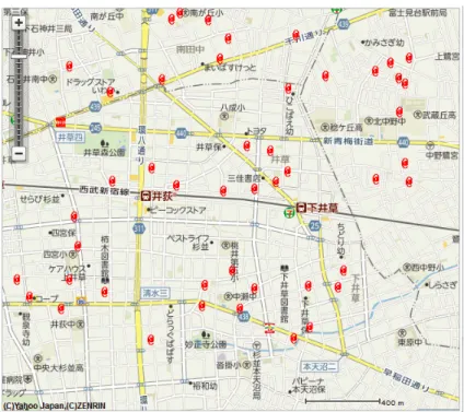
From the measurement results, because the 952 MHz LTE mobile phone signal is the strongest signal at measurement position, so it is the target signal of the proposed RFEH rectenna system. Besides, as indicated in Fig 2.3, RF signals from 4G cell phone base stations are widespread in the ambient environment today. Hence, the cell phone RF energy is one of the ideal energy sources for ambient RFEH.
Figure 2.3: The distribution of mobile phone base station in Tokyo.
2.2
Technical background
2.2.1
Energy requirement of wireless sensor node for
IoT applications
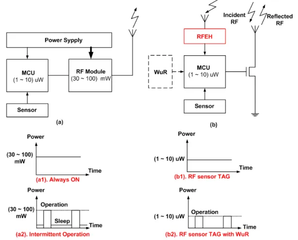
The structures of wireless sensor node (WSN) are presented in Fig 2.4. Figure (a) shows a normal structure of the sensor node which consists of parts such as sensor, micro-control unit (MCU), RF module and power supply. The RF module consumes mainly the power of the sensor node to supply for an RF oscillator and power amplifier of the module. At always ON operation mode, the sensor node always transmits so the power consumption is large, which is
2.2. Technical background
in range of (30 ⇠ 100) mW in general. To reduce power consumption, the RF signal is only transmitted when the information needs to be transferred. The sensor node works in this mechanism is called an intermittent mode. The RF sensor TAG, which shows in Fig 2.4, consumes a very low power because in this structure there is no need to use the RF module. The RF sensor TAG utilizes incident RF signals to transmits information. The power consumption of the RF sensor TAG is minimized by using a wake-up receiver (WuR) unit.
Figure 2.4: Structures of WSNs: (a) Sensor node, and (b) RF sensor TAG powered by RFEH with/without WuR.
Table 2.2 presents power requirements of WSN structures for IoT appli-cations. The WPT technique is chosen depending on the power requirement of WSN. With ambient RFEH, because the level of RF signal in the environ-ment is at µW level so the power that RF energy harvester can generate is at µW level. Therefore, the RF sensor TAG and RF sensor TAG with WuR are
suitable for utilizing ambient RFEH.
Table 2.2: Power requirement of WSN structures for IoT applications.
Sensor mode structure Required power
(a1) Sensor node at always ON mode 30 ⇠ 100 mW [37], [38] (a2) Sensor node at intermittent operation
mode
0.1 ⇠ 1 mW [39], [40]
(b1) RF sensor TAG < 10 µ W [41]
(b2) RF sensor TAG with WuR < 1 µ W [42]
2.2.2
RFEH technique
The ambient RFEH system utilizes available RF energy in the environment so that the system consists of an energy receiver part. A general structure of the RFEH system includes an antenna and a rectifier circuit; hence, the system also called a rectenna. The block diagram and equivalent circuit of the rectenna is presented in Fig 2.5
Figure 2.5: Block diagram and equivalent circuit of RFEH rectenna: (a) Block diagram, and (b) Equivalent circuit
In the system, an antenna is used to receive an RF electromagnetic signal in the environment, change it to an RF electrical signal, and supply the RF signal to the following parts of the system. The rectifier, which is used to convert an RF signal to a DC signal, is a main part of the rectenna system. The efficiency of the rectifier decides the efficiency of the total rectenna system. Generally, RF signal available in the environment at µW level, which is smaller than
2.2. Technical background
a threshold voltage (Vth) of the rectifier component, resulting in significant
decreases in power conversion efficiency (PCE) of the rectifier and the total rectenna system. A matching circuit is utilized to ensure impedance matching between the antenna and the rectifier so that all received power from the antenna is transfer to the rectifier, and reflected power is minimized. The output of the RFEH system is stored in a energy store unit which is general a high capacity capacitor.
There are a large number of study to increase PCE of the RFEH rectenna system, and a majority of the studies is improving implement of separate parts of the RFEH system. Some researches propose solutions to boost the PCE of the rectifier by applying various device technologies or proposing new devices to the rectifier circuit [43–45]. The other studies propose improving architecture of the rectifier such as static Vth cancellation scheme [46], di↵erential-drive
topology [47–49], and floating sub-circuit bias [50].
In solutions to improve the PCE from antenna design, some authors pro-posed solutions to collect RF signals in the environment by gathering a band ambient RF signal such as designing antennas. In the multi-antennas, each antenna is a high Q antenna at each frequency of the target RF signals in the environment [22]. Besides, some studies propose designs of multi-band antennas or broadmulti-band antennas in which the antenna can receive all the target RF signal bands [35,51–54]. Multi-band matching circuit was proposed in some studies to match with multi-band antenna in the RFEH [36,56]
Recent years, study on total RFEH system was proposed in some studies in which the systems can be a single band or multi-band harvesting system. Besdies, some researchers proposed a multi-rectenna system in which recten-nas are combined to synthesize the output DC power [57]. Related to single band rectenna, a co-design rectenna, in which antenna is designed to match with rectifier, was proposed and demonstrated outstanding results in terms of sensitivity and PCE [58,59]. The recent state of art in the RFEH studies is shown as in the Fig 2.6. The survey presents the studies from [33,48,51,58–83]
Figure 2.6: Recent state of art in the RFEH studies
2.2.3
Related studies on ambient RFEH
Although there are many studies about the RFEH system which reach out-standing results in the sensitivity and efficiency of the RFEH system, there is a minority of research that the RFEH rectenna system implements in a real environment. The studies, in which the results of the system measured in a real environment, are listed in table 2.3.
The studies in the table harvested the RF signal from various sources such as TV signal, mobile phone signal, Wi-Fi signal, or multi-signal. Structures of the rectenna systems are also diversity from a single rectenna, multi-band rectenna, and co-design rectenna. In [35,57], the multi-rectenna is utilized as a solution to improve the efficiency of the rectenna. In [35], two rectennas connected in cascade to harvest a mobile phone signal at 845 MHz. In [57], five rectennas are combined to harvest RF signals in 5 bands. In [77], a high impedance antenna is used to improve the PCE due to the high RF voltage fed to the rectifier. The antenna is designed to be a wide bandwidth antenna to receive full bandwidth DTV signal at 500 MHz bands. In [58,80], co-design rectenna is utilized. In these studies, high Q antennas are designed to match with high Q rectifier to improve efficiency of the systems.
2.2. Technical background
Table 2.3: Studies about ambient RFEH.
Antenna Rectifier Matching
circuit Measurement with CW signal from SG or RFDS Measurement with RF ambi-ent signal Kitazawa [35] Dipole an-tenna 6-stage charge pump (Schot-tky diode HSB276AS) Unspecified circuit With SG at 900MHz: 0.79V, 19.7% @ Pin = 5dBm, RL= 10k⌦, Mobile phone 845MHz: 0.32V, 0.22µW @ Pin= 20dBm Kitazawa [57]
Wire and tape folded dipole 2-stage charge pump/band (diode HSMS285C) LC matching network With SG: 9.1%@Pin = 20dBm, 215MHz 5 bands: 1.9 µW @ Pin= 15dBm Stoopman [58] Square loop microstrip antenna 5-stage CCR (90nm CMOS) Control loop by capacitor bank In chamber room: 1V@ -27dBm, open load; 40%@-17dBm; 1V@27m A phone call GSM 900: -4.6dBm, 2m distance: 2.2 V@ 25 seconds, 350 nF capacitor Furuta [77] High impedance dipole an-tenna 2-stage Cockcroft-Walton LC matching network With AR-FEH 500 MHz: 49.8% @ Pin = 15dBm DTV signal: 22.53 µW @ Pin= 13dBm Sadagopan [80] High Q loop antenna 6-stage CCR (GP 65nm CMOS) - RFDS: 1V@-36dBm, 2.4 GHz (primary mode) Wi-Fi 2.42 GHz: 3.3 nW@ Pin = 18.6dBm
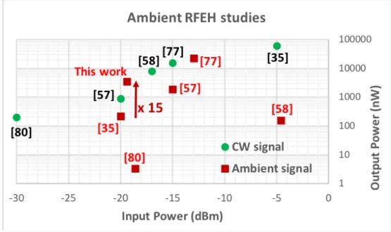
In the studies in table 2.3, the rectenna mostly tested with continuous sine waves (CW) signals in the laboratory. Measurement with RF signal in the environment is implemented in a very short time, and evaluation conditions are extremely unclear. Figure 2.7 presents measurement results of the ambient RFEH studies when the system harvest (CW) signals in the laboratory and real ambient RF signals in the environment. As shown in the figure, output powers
of the studies when harvest real RF signals in the environment are much smaller than that of the case harvesting CW signals in laboratory measurement.
Figure 2.7: Recent state of art in the ambient RFEH studies
The results indicate that the characteristics of the real RF signal in the ambient environment strong a↵ect on the efficiency of the ambient RFEH rectenna system. In conclusion, to design the structure of the ambient RFEH rectenna system, the relationship between characteristics of the ambient RF signal and specifications of the RFEH rectenna must be analyzed.
2.3
The proposed technique of the study
2.3.1
The proposed technique for ambient RFEH
sys-tem
In ambient RFEH, the rectenna harvests RF signal available in the environ-ment to generate DC power, so characteristics of the RF signal decide specifi-cations of the rectenna system. There are two main characteristics of the RF signal that system design of RFEH rectenna must be considered as presented in Fig 2.8:
2.3. The proposed technique of the study • Level of the RF signal.
• Modulation type of the RF signal.
Figure 2.8: Ambient RFEH technique
The level of ambient RF signal in the environment is at µW level, therefore the ambient RFEH system has to work efficiently at this level. Many tech-niques are proposed such as synthesis the signals, reduction threshold voltage of MOSFETs, and high Q rectenna. The high Q rectenna system, in which a high Q antenna and high Q rectifier are designed, shows a prominent result. The passive voltage gain, which is proportion with the Q factor, is high, re-sulting input voltage of the rectifier increasing. Hence, the efficiency of the rectenna system improves. In recent times, researchers tend to design the RFEH rectenna system in which the Q factor is increased. In [58,80], Q fac-tors of antenna are 81 and 120, respectively. Sensitivities in these studies are outstanding values, which are 1V at -27 dBm and -36 dBm, respectively.
Related to waveform modulation of the ambient RF signal, there are two characteristics that a↵ects to the efficiency of the rectenna which are waveform excitation and bandwidth BW. The e↵ect of the waveform excitation of RF signal to the performance of the RFEH system is mentioned in [84–86]. In these studies, theoretical analyzation or measured evaluation was performed just in the rectifier circuit. The e↵ect of the waveform excitation of the RF signal to the performance of the total ambient RFEH rectenna has not mentioned in any related study. In the ambient RFEH, the RF signal is available in
the environment, hence the waveform excitation is not a specification that the system can manage.
In this study, we point out the required specifications of the ambient RFEH system in which the relation of the Q factor of RFEH system and BW of RF signal should be considered simultaneously.
The relationship between Q factor and BW is shown as in equation 2.1 [87,88] Q = !c ✓ Es PD ◆ or Q = fc f = fc f2 f1 (2.1) where Es is energy stored in the circuit, PD is average power dissipated in
the circuit, !c is the resonant frequency in radians/second, fc is the resonant
frequency in Hz, and f is the BW.
The BW of the system can be determined by the reflection coefficient as indicated in Fig 2.9.
Figure 2.9: Definition of BW on the reflection coefficient to calculate Q factor of the system
In the figure, frequencies f1 and f2 are determined at which the return loss
RL1 is calculated by equation 2.2. RL1 = 10log 10 RL0 10 + 1 2 ! (2.2) The Q factor followed by 2.1 is a limited value to ensure the bandwidth of the target ambient RF signal. If the Q factor of the system is larger than the
2.3. The proposed technique of the study
value of Q in equation 2.1, then BW of the system is smaller than BW of the RF signal resulting in power loss.
In the ambient RFEH technique, the Q factor of the RFEH system should be limited by BW of the target RF signal in the ambient environment so that no power loss. The solution to maximizing the Q factor of the RFEH system is not valid with the ambient RF signal. For this reason, in [58,80], output powers are outstanding with the CW signal, but that of the case harvesting real RF signals in the environment dramatically decreases.
In conclusion, to efficient harvest RF signal in the ambient environment, in this study, we propose the structure of the RFEH rectenna that consists of three main characteristics:
• Wide bandwidth RFEH system: BW of the system has to be large enough to cover BW of the target RF signal. Therefore, the Q factor of the RFEH is limited by BW following equation 2.1
• Q factor of rectifier dominates Q factor of the RFEH rectenna system to minimize power loss.
• Rectifier circuit works efficiently in µW level, and Q factor of the rectifier is chosen to ensure BW of the target RF signal
2.3.2
Required specifications of the proposed RFEH
sys-tem
From the designed methodology, two RFEH rectennas was designed to harvest the 950 MHz LTE signal. The specific specifications of the designed RFEH rectenna system are:
• Target RF signal is LTE signal with OFDM modulation at 950 MHz band, from 945 MHz to 960 MHz
• Bandwidth of the RF signal is 15 MHz. The BW of the rectenna is chosen 20 MHz at least to ensure discrepancy.
• Q factor of the rectifier, which calculated follow equation 2.1, is maximum 47. The Q factor of the RFEH system is as much as the Q factor of the rectifier.
• Target application of the study is to supply power for RF sensor TAG and RF sensor TAG with WuR. Therefore, output power of the designed system are required in a µW level.
Chapter 3
Rectifier circuit
3.1
Types of rectifier circuits
3.1.1
Half-wave rectifier
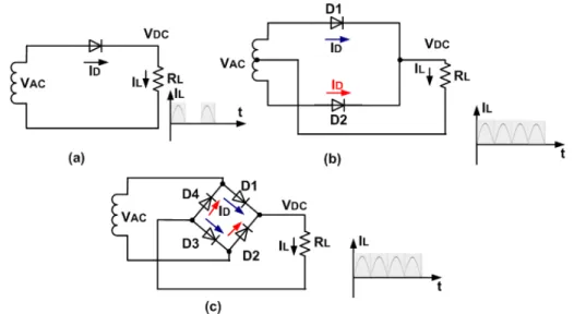
A rectifier is a circuit which converts alternative current (AC) signal to direct current (DC ) signal. The circuit uses components, which enables current in only one direction, such as a diode, transistor. The simplest rectifier circuit, which consists of a diode, an ac source, and a resistive load, is presented in Fig 3.1. First, we consider the circuit in a simple condition to figure out some specifications of the circuit. Input source is an AC source, which generates a sine wave signal. The diode has zero resistance in the forward direction and infinite resistance in the reverse direction. The input voltage and the diode current are shown in Fig. 3.1 (b) and (c).
Figure 3.1: Half-wave rectifier circuits with resistive loads: (a) Half-wave rec-tifier, (b) Wave form of input voltage, and (c) Wave form of diode current
The excited voltage is VAC = VMsin(!t), and a root mean square (RMS)
of the voltage is VRF RM S = VM/
p
2. The excited current is IAC = IMsin(!t),
and RMS of the current is IRF RM S = IM/
p
2. In the half-wave rectifier (HWR), the current only flows into the load in the forward direction when the input voltage is positive, in the reverse direction, the current is nearly zero because of infinite resistance of the diode. Therefore, the output voltage in the load only has one direction. Specifications of the rectifier are listed as follow: [89]
DC current in load current is an average of the load current, which is calculated by equation 3.1 IDC = IAV = 1 2⇡ Z ⇡ 0 IMsin (!t) d (!t) = IM ⇡ ⇡ 0.38IM (3.1)
The RMS of diode current is ID RM S = s 1 2⇡ Z 2⇡ 0 I2 ACd (!t) = s 1 2⇡ Z ⇡ 0 I2 Msin2(!t) d (!t) = IM 2 (3.2) Form factor is the ratio between the RMS and the average. Form factor of the diode current in HWR is
F = IRF RM S IAV
= 0.5IM 0.318IM
= 1.57 (3.3)
Ripple Factor. The rectifier is a nonlinear circuit, so the output of the rectifier consists of DC component, first-order frequency, and harmonic fre-quencies. These components make ripples in the output. The ripples can smooth by using a filter in the output. The ripple factor is calculated by
rf =
Ef f ecitve rectif ied AC load components
Average load current =
p
F2 1 (3.4)
For HWR, rf = 1.21
Power conversion efficiency (PCE), which indicates the ability of the rectifier to convert AC power into DC power, calculated by the ratio of output DC power to AC input power. The maximum PCE of the HWR is shown in 3.5 P CE = PDC PAC = I 2 DCRL I2 RM SRL = 0.405 (3.5)
3.1. Types of rectifier circuits
In conclusion, the HWR uses to rectify a half-wave of the RF signal. Besides, another half-wave power has not been utilized to produce the output; hence, the PCE of the HWR is not high, which is a maximum of 40.5 %. Main advantages of HWR are:
• Simple: circuit structure and number of components;
• Low cost: because of using fewer components in comparison with other rectifier structures.
Disadvantages of HWR are:
• Power loss: the circuit utilizes the power of one-half cycle of the RF signal, and waste the power of the remaining half cycle;
• Low output voltage in comparison to other rectifier structures; • High ripple in the output.
Applications of HWR:
• For rectification applications; • For demodulation applications; • For signal peak applications.
3.1.2
Full-wave rectifier
For rectification applications, to increase rectified efficiency, a full-wave rectifier is used. Fig 3.2 shows schematic diagram of some basic rectifiers.
Figure 3.2: Basic rectifier circuits with resistive loads: (a) Half-wave rectifier, (b) Full-wave center-tap rectifier, and (c) Full-wave bridge rectifier
In a full-wave rectifier (FR) and full-wave bridge rectifier (FBR), two half cycles of the RF signal are utilized to generate DC output power. In FR, diode D1 is in a forward direction in a half cycle while diode D2 is in the forward direction in the remained cycle. In FBR, diode D1 and D3 work in one-half cycle while diode D2 and D4 work in another half cycle. The current in the load resistor is combined with currents in diodes, as shown in fig 3.2. Specifications of the full-wave rectifiers are indicated in table 3.2
Table 3.1: Characteristics of basic rectifier circuits with resistive load
Half-wave rectifier Full-wave rectifier Full-wave bridge
rectifier
Diode average current 0.318IM 0.636IM 0.636IM
Diode rms current 0.5IM 0.707IM 0.707IM
Form factor of diode 1.57 1.57 1.57
Form factor of Load current 1.57 1.11 1.11
Ripple 1.21 0.48 0.48
Maximum PCE (%) 40.6 81.2 81.2
From table 3.2, full-wave rectifiers show better performance in comparison with the half-wave rectifier, especially in PCE. In the full-wave rectifier, the total cycle of the signal is used to generate output signal so that PCE of the
3.1. Types of rectifier circuits
rectifier increases while ripple decreases. The main disadvantage of the full-wave center-tap rectifier is the requirement of using center-tap transformer; while, the main disadvantage of the full-wave bridge rectifier the requirement of using more diodes than other rectifier circuits.
A voltage multiplier rectifier circuit has a high voltage ratio, low voltage stress, high-efficiency [90,91]. Two common types of voltage multiplier rec-tifier circuits are the Cockcroft-Walt recrec-tifier and the Dickson charge pump rectifier, which shown in Fig. 3.3. The Cockcroft-Walton rectifier is a combi-nation of voltage multiplier circuits in series, while, Dickson charge pump is a combination of voltage multiplier circuits in parallel.
Figure 3.3: Schematic of multiplier rectifiers: (a) 3-stage Cockcroft-Walton multiplier rectifier, and (b) 3-stage Dickson charge pump rectifier
3.1.3
MOSFET rectifier for RFEH system
In a conventional rectifier, the Schottky diode is an attractive candidate to utilize in the rectifier circuit due to low forward voltage drop and fast switch-ing speed. However, Schottky diode can not properly be modeled in all CMOS technologies, which shows powerful usefulness in low-cost applications, where high integration levels are desired [92,93]. In recent times, researchers have been best desired to replace Schottky through CMOS technology in the recti-fier circuit. In IoT applications, CMOS technology is a preferred technology because of integrated ability into sensors. In addition, in a low input power range, as shown in Fig. 2.6 in chapter 2, results have got from CMOS technol-ogy in RFEH show satisfactory in comparison with the results got from using Schottky diode.
CMOS technology was successfully applied into many structure of rectifier circuit such as Dickson charge pump [62,91], static Vth cancellation rectifier
[46], cross-coupled rectifier (CCR) [47]. Schematic diagrams of CMOS Dickson charge pump and CCR are shown in Fig 3.4
(a) (b)
Figure 3.4: CMOS rectifier circuits: (a) Dickson charge pump rectifier, and (b) Cross-coupled rectifier CCR
In a low input level range, which can compare to the threshold voltage Vth of the diode/MOSFET, the cross-coupled structure shows an advantage in
3.1. Types of rectifier circuits
Fig 3.4, diode-connected PMOS turns on only when Vin VDC Vth where
Vin= VIN RF + VIN RF . Besides, in CCR, P1 or P2 turns on when Vin Vth,
which means circuit can work at a low input level. In summary, the CMOS CCR is a popular choice of researchers in order to design RFEH systems for IoT applications.
In a CCR, a couple of cross MOSFET works in a half cycle of the RF signal, the other couple of MOSFET works in a remained half cycle. For instance, in Fig 3.4 (b), when positive half cycle is supplied into INRF+, PMOS P1 and
NMOS N2 will turn on, while P2 and N1 turn o↵. Currents in the circuit flow
follow the black arrow. In a half-cycle after, the currents flow in the direction of the red arrow. The operation principle of CCR is the same as the full-wave bridge rectifier, so the efficiency of CCR is improved.
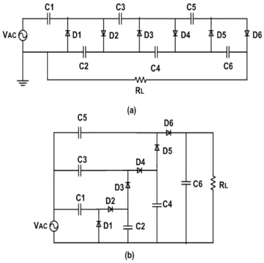
Base on CCR, [50] proposed the structure of CCR with floating sub-circuits, which has a schematic shown in Fig 3.5.
In one stage of CCR with floating sub-circuits, there are three CCRs which are the main CCR and two CCR sub-circuits. Each CCR sub-circuit has an open load so that DC level at point OP1 (or OP2) is maximized. Hence, DC levels at FL11, and FL12, which are almost half of OP1, are also maximized. These voltages are supplied to the gates of the MOSFETs in the main CC. Hence, in comparison to a conventional CCR, CCR with floating sub-circuits reaches a higher gate-to-source voltage of MOSFET in the main CCR, as indicated in equation 3.6.
VGS(N 1) = Vin+ V DC (3.6)
where V DC is a DC di↵erence level of the voltages at FL12 and M1. The voltage V DC shows the e↵ectiveness of CCR with floating sub-circuits in comparison to a conventional CCR.
In this study, CCR and CCR with floating sub-circuits are utilized to de-signed rectifier circuit on an application of 65nm Silicon-On-Thin Buried Oxide (SOTB) technology.
The SOTB, which is one of the FD-SOI CMOS processes, has been de-veloped recently due to its advantages in comparison to a conventional bulk CMOS [94,95]. In [95], the RF characteristics of 65 nm SOTB CMOS are measured and presented as shown in table 3.2.
Table 3.2: RF characteristics of 65 nm SOTB [101]
PMOS NMOS
Gate length 60 nm 60 nm
Gate oxide thickness 2.0 nm 2.0 nm
Threshold Voltage -0.32 V 0.35V
FT 26 GHz 40 GHz
Fmax 20 GHz 28 GHz
As indicated from the table, because Fmax of PMOS and NMOS of SOTB
devices are 20 GHz and 28 GHz, respectively, so, it is indicated that the SOTB technology works e↵ectively at 1 GHz frequency range.
3.2. Principle specifications a↵ect to efficiency of rectifier
3.2
Principle specifications a↵ect to efficiency
of rectifier
3.2.1
Drain current
The relationship between drain current and output of the rectifier is indicated from a current-voltage relationship in CCR. A single-stage schematic of CCR is shown in Figure 3.6. IV relation in NMOS N1 is considered to simplify the work of CCR. Positive drain current in N1 is a forward current that charges the load. In contract, negative drain current in N1 is the flow-back current that discharges the load.
Figure 3.6: Schematic of a single stage CCR
RF di↵erential signals at V1 and V2 are supplied by AC source through
cou-pling capacitor Cc and can be denoted by VRFsin2⇡f t and VRFsin (2⇡f t + ⇡),
respectively. V1 and V2 also have DC voltages. We denote these voltages are
DCof f set voltages. Consider CCR is symmetrically designed, so voltages at V1,
V2 have the same absolute value and can be express as equation 3.7, 3.8. Due
to the symmetry of CMOS devices, the drain and source of MOSFET can be switched depending on the potentials at these ports.
V1 = VDC of f set+ VRFsin2⇡f t (3.7)
If V1 0 which is equivalent to sin2⇡ft VDC of f setVRF , then VGS and VDS
through N1 are:
VGS = V2 V1 = 2VRFsin2⇡f t if V1 0 (3.9)
VDS = V1 = VRFsin2⇡f t (3.10)
If V1 > 0 which is equivalent to sin2⇡f t > VDC of f setVRF , then VGS and VDS
through N1 are:
VGS = V2 = VRFsin (2⇡f t + ⇡) if V1 > 0 (3.11)
VDS = V1 = VRFsin2⇡f t if V1 > 0 (3.12)
Depend on the gate-source VGS voltage and drain-source VDS voltage,
MOS-FET works in one of three regions: week inversion region, triode region, satu-ration region [96].
Current in week inversion region, when VGS < Vth, is calculated by
ID W I = W L Itexp ✓ VGS Vth nVT ◆ 1 exp ✓ VDS VT ◆ (3.13) where It is a drain current when VGS = Vth, W/L = 1, and VDS VT;
n = (1 + Cjx/Cox) is a voltage division between the oxide capacitance Cox
and depletion-region capacitance Cjs; VT is a thermal voltage, which is nearly
26mV at room temperature. Denote Is0 is Is0 = W LItexp ✓ Vth nVT ◆ (3.14) then ID W I can rewrite as
ID W I = Is0exp ✓ VGS nVT ◆ 1 exp ✓ VDS VT ◆ (3.15) Current in triode region
ID T = k0 2 W L ⇥ 2 (VGS Vth) VDS VDS2 ⇤ (3.16)
3.2. Principle specifications a↵ect to efficiency of rectifier where k0 = µnCox = µn"toxox
Current in saturation mode ID S = k0 2 W L(VGS Vth) 2 (1 + VDS) (3.17)
where is a channel-length modulation coefficient.
The current flows in load is a combined current in two branches of the CCR. The DC output current is an integral of the load current, which calculated by equation 3.18. The output voltage and power are calculated by equation 3.19, 3.20 IDC = IAV = 1 T Z T 0 ILdt = 1 T Z T 0 2IDdt (3.18) VDC = IDCRL (3.19) Pout= 1 T Z T 0 IL2RLdt (3.20)
In a low input level, VRF < Vth, so the MOSFETs usually work in the
weak-inversion region. Therefore, the drain current is mainly calculated by equation 3.15. The equation indicates that current in this region depends on Is0, VGS,
and VDS. Is0 presents characteristics of the MOSFET, while VGS and VDS
depend on levels of the RF signal. It can conclude that Is0 increases letting
DC current in load increases.
The driving body of MOSFET is a popular technique to increase the drain current of MOSFET. The dynamic threshold voltage MOSFET (DTMOS) technique, in which the body of the MOSFET is tied to the gate, is an e↵ective technique to drive the drain current. In [97], it has been proved that a very low voltage on the DTMOS technique can obtain a much higher current drain than regular MOSFET. In RFEH technique, DTMOS is utilized to the rectifier as a diode-connected rectifier [98], self Vth cancellation rectifier [99].
In the SOTB technique, the threshold voltage of the MOSFET can be modulated by body bias, such that DTMOS becomes more e↵ective than the
normal MOSFET structure. The body bias constant, which is calculated by equation 3.21, is almost 150 mV/1V in SOTB [100]. In [101,102], we proved the e↵ectiveness of DTMOS in terms of decreasing Vth of the MOSFET in
comparison to body-tired-to-source (BTMOS) in the 65 nm SOTB technique.
↵ = Vth VBS
(3.21) Figure 3.7 present simulated results of IV characteristics in 4 configuration types: diode-connected BTMOS, diode-connected DTMOS, DTMOS in CCR and DTMOS in CCR with floating sub-circuits
Figure 3.7: Simulated IV characteristic of the DTMOS diode, BTMOS diode, DTMOS CCR configuration, and DTMOS CCR with floating sub-circuits con-figuration
The figure indicates that applying DTMOS gains a higher drain current than BTMOS. Besides, as shown in the figure, in DTMOS CCR and CTMOS CCR with floating sub-circuit, the drain current is much higher than a diode-connected configuration. In simulation conditions, a 63 mV DC voltage of CCR floating sub-circuit is the amount of V DC that the circuit achieved when input power is -20 dBm, as presented in Fig 3.8.
3.2. Principle specifications a↵ect to efficiency of rectifier -30 -25 -20 -15 -10 -5 Input RF power (dBm) 10 20 30 40 50 60 70 VDC (mV)
DC voltage boosted from floating sub-circuit
63 mV
Figure 3.8: Simulated DC level-up amount ( V DC) from the floating sub-circuit
Fig 3.9 shows the simulated the dependence of output power of the rectifier on Is0. As in equation 3.15, Is0 presents the characteristics of the MOSFET on
weak inversion region. The simulated results got from a conditions that input power is -20 dBm, and load is 100k⌦
Figure 3.9: Simulated the dependence of output power of the rectifier on Is0
As shown in the figure, the output power of the CCR with floating sub-circuit is the highest because of the drain current of this structure is the highest. To conclude, DTMOS CCR and DTMOS CCR with floating sub-circuit on 65 nm SOTB technique is the best choice for the low input level range. The rectifiers in this study are chosen from these structures.
3.2.2
Q factor
The Q factor of a resonator, which is also a passive gain, is calculated by equa-tion 2.1 in relaequa-tionship with power and bandwidth of the resonator. Besides, in a relationship with resistance and reactance of the resonator at a resonant frequency, Q factor can be calculated by:
Q = X R =
B
G (3.22)
where R, X, G, B are resistance, reactance, susceptance, conductance of the resonator.
In the RFEH rectenna, when a matching condition between antenna and rectifier is satisfied, the system is equivalent to a resonator, and at this con-dition, the passive gain Q will achieve. In chapter 2, the limitation of the Q factor of the rectifier to ensure BW of RF signal is proved. In this section, the relationship between the Q factor and the number of CCR stages is pre-sented. First, the e↵ect of the Q factor on the input voltage of the rectifier is considered. A equivalent of the rectifier is shown in Fig 3.10 to simplify analysis.
Figure 3.10: Equivalent circuit of a rectifier in the RFEH rectenna
A condition to ensure matching happen is analyzed in Chapter 4. In this section, we consider that matching condition is satisfied so that a source VS
supplies a power Prect to the rectifier. At this condition, from input view,
3.2. Principle specifications a↵ect to efficiency of rectifier Prect, Crect, Rrect, Vrect are shown in equation 3.23, 3.24, 3.25
Qrect = Brect Grect = !CrectRrect (3.23) Prect= V2 rect |Zrect| cos (✓) = V 2 rect Grect(1 + Q2rect) (3.24) Vrect= q
PrectGrect(1 + Q2rect) (3.25)
From equation 3.25, Vrect is proportion with Qrect. With the same input
power Prect value, Qrect is higher resulting Vrect higher; hence output is higher.
The output voltage of the rectifier also increases when number of rectifier stage increase. The block diagram of n-stage CCR is shown in Fig 3.11
Figure 3.11: Block diagram of N stage CCR
In n-stage CCR, the RF signal is supplied in parallel while the DC signal is added in serial through n stages. If RF power supplied into each stage is unchanged, so the output of n-stage is equal to n times of one stage. However, because n-stage is connected in parallel, so input impedance of rectifier Zrect
also changes. To analyze the Q factor in n-stage, first, we consider a small-signal model of MOSFET as Fig. 3.12 [87], [103]