• 検索結果がありません。

PowerPoint プレゼンテーション

N/A
N/A
Protected

Academic year: 2021

シェア "PowerPoint プレゼンテーション"

Copied!
21
0
0

読み込み中.... (全文を見る)

全文

(1)

Lithography WG活動報告

「ITRS 2015に見る

リソグラフィ技術の最新動向」

STRJ WS

2016年3月4日

品川:コクヨホール

WG5主査:上澤 史且(ソニー)

(2)

WG5(リソグラフィWG)の活動体制

- JEITA半導体部会/関連会社 -

 上澤 史且(ソニー)/リーダー

 小林 幸子(東芝) /サブリーダー

 千々松 達夫(ソシオネクスト)

 竹田 裕史(ローム)

 山本 次朗(日立製作所)

-コンソーシアム-

 東 司(EIDEC)

- SEAJ 他 -

 奥村 正彦/国際委員(SEAJ:ニコン)

 高橋 和弘(SEAJ:キヤノン)

 中島 英男(SEAJ:TEL)

 山口 哲男(SEAJ:ニューフレアテクノロジー)

 笠間 邦彦(SEAJ:ウシオ電機)

 大久保 靖(HOYA)

 林 直也 (大日本印刷)

 小西 敏雄(凸版印刷)

 大森 克実(東京応化工業)

 栗原 啓志郎(アライアンスコア)

 遠藤 政孝(大阪大学)

計17名

(3)

微細化の目的の1つはチップコスト削減

¥13,970

(2015/5/25)

¥9,439

(2015/11/30)

半年で32%も下落!

微細化

→ チップ面積縮小 → 理収増加 → チップコスト削減

256G Byte SDカードの価格推移例

(4)

Year of Production 2015 2017 2019 2021 2024 2027

DRAM

DRAM minimum ½ pitch (nm) 24 22 18.0 15.0 12.0 9.2

CD control (3 sigma) (nm) [B] 2.4 2.2 1.8 1.5 1.2 0.9

Mininum contact/via after etch (nm) [H] 24 22 18 15 12.0 9.2

Minimum contact/via pitch(nm)[H] 72 66 54 45 36 28

Overlay (3 sigma) (nm) [A] 4.8 4.4 3.6 3.0 2.4 1.8

Flash

2D Flash ½ pitch (nm) (un-contacted poly) 15 14 12 12 12 12

Flash 3D Layer half-pitch targets (nm) 80.0 80.0 80.0 80.0 80.0 80.0

3D NAND minimum metal pitch(nm) 20.0 20.0 20.0 20.0 20.0 20.0

CD control (3 sigma) (nm) [B] 1.5 1.4 1.2 1.2 1.2 1.2

Overlay (3 sigma) (nm) [A] 5.1 4.7 3.9 3.9 3.9 3.9

MPU / Logic

MPU/ASIC Minimum Metal ½ pitch (nm) 26 18 12 10 6.0 6.0

MPU/ASIC finFET fin minimum 1/2 pitch (nm) 21 18 12

Lateral Gate All Around (LGAA) 1/2 pitch 12 10

Vertical Gate All Around (VGAA) 1/2 pitch 10 6.0 6.0

Contacted poly half pitch (nm) 35 24 21 16

Physical Gate Length for HP Logic (nm) 24 18 14 10

Vertical Gate All Around (VGAA) pitch (nm) 20 12 12

Gate CD control (3 sigma) (nm) [B] 2.4 1.8 1.4 1.0

Metal CD control (3 sigma) (nm) [B] 2.6 1.8 1.2 1.0 0.6 0.6

Fin CD control (3 sigma) (nm) [B] 0.40 0.30 0.30

FIN or LGAA LER [C] 0.40 0.30 0.30

Gate LER [C] 2.4 1.8 1.4 1.0

Metal LWR [C] 3.9 2.7 1.8 1.5 0.9 0.9

Vertical GAA Diameter (nm) 6 5 5

MPU/ASIC minimum contact hole or via pitch (nm) 74 51 34 28 17 17

Contact/via CD after etch (nm) [H] 26 18 12 10 6.0 6.0

Contact CD (nm) - finFET, LGAA 22 14 16 12 11.0 11.0

Vertical Gate All Around (VGAA) diameter (nm) 10 6.0 6.0

Overlay (3 sigma) (nm) [A} 5.2 3.6 2.4 2.0 1.2 1.2

Chip size (mm2)

Maximum exposure field height (mm) [E] 26 26 26 26 26 26

ITRSのロードマップ(Lithography)

N10

チップコストの削減を目的に微細化が着々と続けられている

N7

N5

N3.5

(5)

微細化によるチップコストの削減効果

インテル社の発表資料より抜粋

(6)

リソグラフィの解像度向上の歴史

NA

k

1

λ

=

解像度

(k

1

~0.4)

リソグラフィの高解像度化は、光源波長(λ)の短波長化と投影レンズの

高NA化により達成されてきており、次世代リソの最有力候補がEUV。

0

50

100

150

200

250

1990

1995

2000

2005

2010

2015

i-line

KrF

ArF

ArF液浸

EUV

解像度

NA=0.63

NA=0.55

NA=0.60

NA=0.68

NA=0.75

NA=0.82

NA=0.86

NA=0.60

NA=0.68

NA=0.78

NA=0.85

NA=0.93

NA=1.20

NA=1.30

NA=1.35

NA=0.25

λ=365nm)

λ=248nm)

λ=193nm)

λ=13.5nm)

NA=0.33

(7)

EUVリソグラフィの課題

光源

レジスト

無欠陥マスク

ペリクル

光源、レジスト、無欠陥マスク、ペリクルがEUVリソの4大課題

(8)

EUV光源出力の現状

量産には250Wが必要と言われているが現状は100W程度の出力

(9)

EUVマスクの課題

【EUV用ペリクル】

【課題】

・透過率目標90%に対して現状は85%

(50nm厚のpoly-Siで作製)

・仮に90%達成できても、往復では81%に光量

が減衰してしまう

・露光中の蓄熱により温度が1000℃以上に

上昇してしまうとの報告あり

【EUVマスク】

【特徴】

・数nmのMo層とSi層を交互に約50層積層し

た多層膜ミラー構造

・デバイスパターンはTa等のEUVを吸収する

材料で描かれている

・多層膜の成膜過程で異物が混入した欠陥

は位相欠陥と呼ばれ、修正が極めて困難

(10)

• 微細化の手段としてはリソグラフィ光源の短波長化であり

高解像度化を実現するための王道路線と言える。

• EUVリソの最大の課題は光源出力の不足で、目標250Wに

対し、現状はまだ100W程度の出力しか得られていない。

• EUVマスクやペリクルにも多くの困難な課題あり。

EUVによる20nmピッチL/Sの形成例(inpria社の発表資料より抜粋)
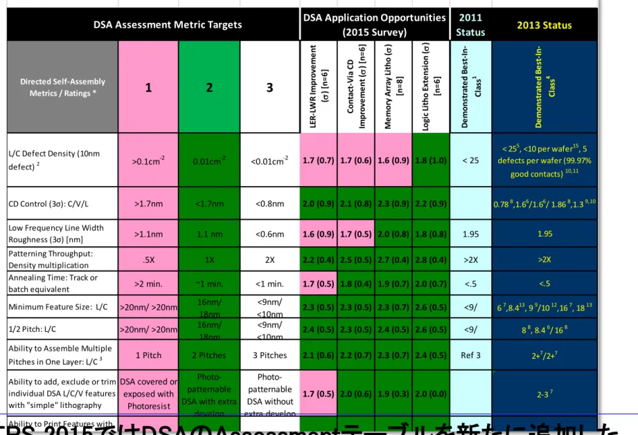
ここまでのまとめ ~EUVリソの現状~

(11)

Year of Production 2015 2017 2019 2021 2024 2027

DRAM

DRAM minimum ½ pitch (nm) 24 22 18.0 15.0 12.0 9.2

CD control (3 sigma) (nm) [B] 2.4 2.2 1.8 1.5 1.2 0.9

Mininum contact/via after etch (nm) [H] 24 22 18 15 12.0 9.2

Minimum contact/via pitch(nm)[H] 72 66 54 45 36 28

Overlay (3 sigma) (nm) [A] 4.8 4.4 3.6 3.0 2.4 1.8

Flash

2D Flash ½ pitch (nm) (un-contacted poly) 15 14 12 12 12 12

Flash 3D Layer half-pitch targets (nm) 80.0 80.0 80.0 80.0 80.0 80.0

3D NAND minimum metal pitch(nm) 20.0 20.0 20.0 20.0 20.0 20.0

CD control (3 sigma) (nm) [B] 1.5 1.4 1.2 1.2 1.2 1.2

Overlay (3 sigma) (nm) [A] 5.1 4.7 3.9 3.9 3.9 3.9

MPU / Logic

MPU/ASIC Minimum Metal ½ pitch (nm) 26 18 12 10 6.0 6.0

MPU/ASIC finFET fin minimum 1/2 pitch (nm) 21 18 12

Lateral Gate All Around (LGAA) 1/2 pitch 12 10

Vertical Gate All Around (VGAA) 1/2 pitch 10 6.0 6.0

Contacted poly half pitch (nm) 35 24 21 16

Physical Gate Length for HP Logic (nm) 24 18 14 10

Vertical Gate All Around (VGAA) pitch (nm) 20 12 12

Gate CD control (3 sigma) (nm) [B] 2.4 1.8 1.4 1.0

Metal CD control (3 sigma) (nm) [B] 2.6 1.8 1.2 1.0 0.6 0.6

Fin CD control (3 sigma) (nm) [B] 0.40 0.30 0.30

FIN or LGAA LER [C] 0.40 0.30 0.30

Gate LER [C] 2.4 1.8 1.4 1.0

Metal LWR [C] 3.9 2.7 1.8 1.5 0.9 0.9

Vertical GAA Diameter (nm) 6 5 5

MPU/ASIC minimum contact hole or via pitch (nm) 74 51 34 28 17 17

Contact/via CD after etch (nm) [H] 26 18 12 10 6.0 6.0

Contact CD (nm) - finFET, LGAA 22 14 16 12 11.0 11.0

Vertical Gate All Around (VGAA) diameter (nm) 10 6.0 6.0

Overlay (3 sigma) (nm) [A} 5.2 3.6 2.4 2.0 1.2 1.2

Chip size (mm2)

Maximum exposure field height (mm) [E] 26 26 26 26 26 26

N7

ITRSのロードマップ(Lithography)

EUVが導入されるのは早くても7nmノードからとなる見込み

N10

N5

N3.5

×

(12)

1st Mask

Etch

Depo

Etch

2nd Cut Mask

3rd Cut Mask

Etch

Depo

SAQP (Self Aligned Quadruple Patterning)

レジスト

40nm L&S

Etch

Etch

10nm L&S

10nm L/30nm S

EUVを用いずに微細化を実現する手段①

SAQPで形成した11nm L&Sパターン

(東京エレクトロンの発表資料より抜粋)

SAOP (Self Aligned Octuplet Patterning)で

形成した6.25nm L&Sパターン

(13)

マルチパターニングによる微細化の追求

(14)

EUVを用いずに微細化を実現する手段②

DSA (Directed Self Assembly):誘導自己組織化

Polymer-A

ex. Poly styrene)

Polymer-B

ex. PMMA)

Block Copolymer

SA

プレパターン

(パターン寸法は材料組成によって制御する)

(15)

DSAを用いた微細パターンの形成(L&Sパターン)

CD=19.2nm

CD=19.2nm

(16)

0

20

40

60

80

2009 2010 2011 2012 2013 2014 2015 2016

DSA関連発表件数

SPIE Advanced Lithography

・近年、最も注目を集めている微細加工技術

・IBMはDSAを用いたFin FETの試作に成功

・ITRS2015ではDSAのAssessment結果を掲載

したテーブルを新たに追加した

・量産適用に向けた最大の課題は欠陥制御

DSAの開発状況

*Hsinyu Tsai, et al., “Electrical Characterization of FinFETs with Fins Formed by Directed Self Assembly at 29 nm Fin Pitch Using a Self-Aligned Fin Customization Scheme,” IEDM 2014.

10nmノードFin FETの

試作に成功!

(Fin pitch: 29nm)

(17)

Work in Progress - Do not publish

STRJ WS: March 4, 2016, WG5 Litho

17

Table LITH3 Directed Self Assembly Critical Assessment (2015)

2011

Status

2013 Status

Directed Self-Assembly

Metrics / Ratings *

1

2

3

LE

R-LW

R I

m

pr

ov

em

en

t

) [

n=

6]

Co

nt

ac

t-Vi

a C

D

Imp

ro

ve

me

nt

) [

n=

6]

M

em

ory

A

rra

y L

ith

o (

σ)

[n

=8

]

Lo

gi

c L

itho

E

xt

ens

io

n (

σ)

[n

=6

]

De

mo

ns

tr

at

ed

B

es

t-In

-Cl

as

s

1

De

mo

ns

tr

at

ed

B

es

t-In

-Cl

as

s

4

L/C Defect Density (10nm

defect)

2

>0.1cm

-2

0.01cm

-2

<0.01cm

-2

1.7 (0.7) 1.7 (0.6) 1.6 (0.9) 1.8 (1.0)

< 25

< 25

5

, <10 per wafer

15

, 5

defects per wafer (99.97%

good contacts)

10,11

CD Control (3σ): C/V/L

>1.7nm

<1.7nm

<0.8nm

2.0 (0.9) 2.1 (0.8) 2.3 (0.9) 2.2 (0.9)

0.78

8

,1.6

6

/1.6

6

/ 1.86

8

,1.3

9,10

Low Frequency Line Width

Roughness (3σ) [nm]

>1.1nm

1.1 nm

<0.6nm

1.6 (0.9) 1.7 (0.5) 2.0 (0.8) 1.8 (0.8)

1.95

1.95

Patterning Throughput:

Density multiplication

.5X

1X

2X

2.2 (0.4) 2.5 (0.5) 2.7 (0.4) 2.8 (0.4)

>2X

>2X

Annealing Time: Track or

batch equivalent

>2 min.

~1 min.

<1 min.

1.7 (0.5) 1.8 (0.4) 1.9 (0.7) 2.0 (0.7)

<.5

<.5

Minimum Feature Size: L/C

>20nm/ >20nm

16nm/

18nm

<10nm

<9nm/

2.3 (0.5) 2.3 (0.5) 2.3 (0.7) 2.6 (0.5)

<9/

6

7

,8.4

13

, 9

9

/10

12

,16

7

, 18

13

1/2 Pitch: L/C

>20nm/ >20nm

16nm/

18nm

<10nm

<9nm/

2.4 (0.5) 2.3 (0.5) 2.4 (0.5) 2.6 (0.5)

<9/

8

8

, 8.4

6

/

16

8

Ability to Assemble Multiple

Pitches in One Layer: L/C

3

1 Pitch

2 Pitches

3 Pitches

2.1 (0.6) 2.2 (0.7) 2.3 (0.7) 2.4 (0.5)

Ref 3

2+

7

/2+

7

Ability to add, exclude or trim

individual DSA L/C/V features

with "simple" lithography

DSA covered or

exposed with

Photoresist

Photo-patternable

DSA with extra

develop

Photo-patternable

DSA without

extra develop

1.7 (0.5) 2.0 (0.6) 1.9 (0.3) 2.0 (0.0)

2-3

7

Ability to Print Features with

DSA Assessment Metric Targets

DSA Application Opportunities

(2015 Survey)

DSAのAssessment Table

(18)

NanoimprintやEB直描を含めた、次世代リソ技術の課題と判断時期を示した

テーブルを作成した。2016年はこれらの技術判断を行う重要な年になると予想。

(19)

次世代リソ技術の性能比較

光源出力の不足による処理能力の

低さが最大の課題

直描故の処理能力の低さと

パターン位置精度が課題

等倍の3Dマスク作製技術や

欠陥制御技術が課題

欠陥制御技術が課題

(20)

 デバイスの高性能化とチップコストの削減を目的に、現在も

微細化技術の開発が着々と続けられている。

 EUVリソは光源を始めとする様々な技術開発が遅れており、

量産に使われるのは早くても7nmノードからとなる見込み。

 新たな微細加工技術としてDSAが注目を集めており、World

Wideで精力的に開発が進められている。

 2016年は次世代リソの技術判断が行われる重要なターニン

グポイントの年になるものと予想される。

まとめ

(21)

略語

AIMS Aerial Image Measurement System

AMC

Airborne Molecular Contamination

ARC

Anti-Reflection Coating

BARC

Bottom ARC

TARC

Top ARC

CAR

Chemical Amplified Resist

CD

Critical Dimension

CDU

CD Uniformity

DE

Double Exposure

DFM

Design for Manufacturing/

Design for Manufacturability

DP/MP

Double Patterning / Multiple Patterning

DPP

Discharged Produces Plasma

DSA

Directed-Self-Assembly

DOF

Depth of Focus

EBDW

Electron Beam Direct Writer

EDA

Electronic Design Automation

EPL

Electron Projection Lithography

ESD

Electro Static Discharge

EUVL

Extreme Ultraviolet Lithography

IPL

Ion Projection Lithography

LDP

Laser assisted Discharge Plasma

LELE

Litho-Etch-Litho-Etch (1kind of DP)

LER

Line Edge Roughness

LPP

Laser Produced Plasma

LTEM

Low Thermal Expansion Material

LWR

Line Width Roughness

MEEF

Mask Error Enhancement Factor (=MEF)

ML2

Maskless Lithography

NA

Numerical Aperture

NGL

Next Generation Lithography

NIL

NanoImprint Lithography

NTD

Negative Tone Development

OAI

Off-Axis Illumination

OPC

Optical Proximity Corrections

RBOPC

Rule Base OPC

MBOPC

Model Base OPC

PSM

Phase Shifting Mask

cPSM

complementary PSM

APSM

Alternating PSM

EPSM

Embedded PSM

Att. PSM

Attenuated PSM

PXL

Proximity X-ray Lithography

RET

Resolution Enhancement Techniques

SADP

Self Aligned DP

SAQP

Self Aligned Quadruple Patterning

SB

Scattering Bar (same meaning as SRAF)

SRAF

Sub Resolution Assist Feature™

SFIL

Step & Flash Imprint Lithography

SMO

Source Mask co-Optimization

UV-NIL

Ultraviolet NIL

Table LITH3   Directed Self Assembly Critical Assessment (2015)

参照

関連したドキュメント

●Gartner Magic QuadrantにてクラウドHCM Suiteにおけるリーダーの評価.. Copyright © 2022 Nomura System Corporation Co, Ltd. All Rights Reserved.. Copyright © 2022 Nomura

An intense electron beam with strong self-field can be compressed using coaxial cavities with decreasing lengths.. An intense electron beam with subnanosecond duration is available

支援要請入力詳細 13ページ 患者受入入力詳細 14ページ 支援可能スタッフ3.

and Kristjan Vassil (2010) Internet voting in Estonia : a comparative analysis of four elections since 2005 : report for the Council of Europe”Report for the Council of Europe.

2021年1月15日にHa Tay Pharmaceutical Joint Stock Company(

がん化学療法に十分な知識・経験を持つ医師のもとで、本剤の投与が適切と判断さ

日医かかりつけ医機能研修制度 令和 年度応用研修会 「メタボリックシンドロームからフレイルまで」 飯島勝矢 Tamakoshi A ら. Obesity

(Immuno Checkpoint Inhibitor Proper use Support team